CrossFire Xpress 3200: RD580 for AM2
by Wesley Fink on June 1, 2006 12:05 AM EST- Posted in
- Motherboards
Overclocking
The initial reference BIOS supplied by ATI was plagued with several issues that limited overclocking. Since RD580 is known to be an excellent overclocker, ATI looked into the issues and supplied a new 5/30/2006 BIOS which corrected the timing issues that had limited overclocking in the first BIOS.
With the Build 15 BIOS, the ATI CrossFire Xpress 3200 AM2 is an outstanding overclocker - the best we have seen at both stock and reduced multiplier overclocking. We made no attempt to maintain memory speed, but instead selected memory ratios that would allow the Corsair test memory to run at the optimal 3-3-3 timings at around DDR2-800. With the DDR2 memory controller on the processor with the AMD AM2, ratios should not really carry performance penalties as they do on chipset based memory controllers.
No attempt was made to run at x8 or x7 multipliers, which theoretically could yield 380x8 or 400 (highest bus speed option) x7 if the processor speed could be maintained. ATI was absolutely correct in their assessment of our early BIOS bug issues. Overclocking with the updated Build 15 BIOS was effortless, with almost no special OC skills required. Most settings were left on auto, except for a slight boost in HTT voltage and a drop to 4X HT. 5x HTT reached to just over 1500 HTT (302) before requiring a drop to 4x. In all cases base memory speed was reduced to a setting that would yield somewhere around DDR2-800 at OC and timings were left at 3-3-3-13 at 2.147v. We did not even need to boost processor voltage until we reached just over 3.0GHz. The AM2 CPU handled the 3.0 GHz speed at stock voltage. These overclocking results are superb.
Power Usage
It has been reported that the ATI RD580 chipset consumes up to 40 watts less power than the feature-comparable nForce590. We attempted to verify these results with our standard Model P4400 Kill-a-watt meter. The Kill-a-watt plugs into the wall and measures wattage of the entire system. We compared near identically configured Foxconn NVIDIA 590 and ATI CrossFire Xpress 3200 AM2 systems at idle and under stress.
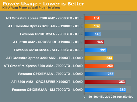
While the ATI system used less power at idle and when stressed, we could not match the 40W difference some others have reported. We did find the ATI system a bit more power efficient running the NVIDIA 7900GTX or the ATI X1900 XT. Even full CrossFire X1900 XT consumed less power in the ATI AM2 board than NVIDIA SLI 7900GTX required in the NVIDIA 590 board.
Power consumption goes up dramatically during overclocking. At the standard 12X multiplier and 255 clock speed (3.06GHz), running X1900 XT Crossfire, power consumption measured over 500 Watts during load conditions. Whether SLI or Crossfire, ATI or NVIDIA, please keep in mind that two top video cards and overclocking require tremendous amounts of power for stable operation.
| ATI CrossFire Xpress 3200 AM2 Overclocking Testbed |
|
| Processor: | AM2 X2 4800+ (2.4GHz, 1MB Cache per core) |
| CPU Voltage: | 1.4V (default 1.3V) |
| Cooling: | AMD Stock Heatpipe FX62 Cooler |
| Power Supply: | OCZ Power Stream 520W |
| Memory: | Corsair Twin2x2048-PC2-8500C5 (2x1GB) (Micron Memory Chips) 2 DIMMs in dual-channel mode |
| Hard Drive: | Hitachi 250GB 7200RPM SATA2 8MB Cache |
| Maximum OC: (Standard Ratio) |
255x12 (5x HT, 3-3-3-13) 3060MHz (+28% CPU Overclock) |
| Maximum FSB: (Lower Ratio) |
338 x 9 (4x HT, 3-3-3-13) 3042MHz (+69% Bus Overclock) |
The initial reference BIOS supplied by ATI was plagued with several issues that limited overclocking. Since RD580 is known to be an excellent overclocker, ATI looked into the issues and supplied a new 5/30/2006 BIOS which corrected the timing issues that had limited overclocking in the first BIOS.
With the Build 15 BIOS, the ATI CrossFire Xpress 3200 AM2 is an outstanding overclocker - the best we have seen at both stock and reduced multiplier overclocking. We made no attempt to maintain memory speed, but instead selected memory ratios that would allow the Corsair test memory to run at the optimal 3-3-3 timings at around DDR2-800. With the DDR2 memory controller on the processor with the AMD AM2, ratios should not really carry performance penalties as they do on chipset based memory controllers.
No attempt was made to run at x8 or x7 multipliers, which theoretically could yield 380x8 or 400 (highest bus speed option) x7 if the processor speed could be maintained. ATI was absolutely correct in their assessment of our early BIOS bug issues. Overclocking with the updated Build 15 BIOS was effortless, with almost no special OC skills required. Most settings were left on auto, except for a slight boost in HTT voltage and a drop to 4X HT. 5x HTT reached to just over 1500 HTT (302) before requiring a drop to 4x. In all cases base memory speed was reduced to a setting that would yield somewhere around DDR2-800 at OC and timings were left at 3-3-3-13 at 2.147v. We did not even need to boost processor voltage until we reached just over 3.0GHz. The AM2 CPU handled the 3.0 GHz speed at stock voltage. These overclocking results are superb.
Power Usage
It has been reported that the ATI RD580 chipset consumes up to 40 watts less power than the feature-comparable nForce590. We attempted to verify these results with our standard Model P4400 Kill-a-watt meter. The Kill-a-watt plugs into the wall and measures wattage of the entire system. We compared near identically configured Foxconn NVIDIA 590 and ATI CrossFire Xpress 3200 AM2 systems at idle and under stress.
While the ATI system used less power at idle and when stressed, we could not match the 40W difference some others have reported. We did find the ATI system a bit more power efficient running the NVIDIA 7900GTX or the ATI X1900 XT. Even full CrossFire X1900 XT consumed less power in the ATI AM2 board than NVIDIA SLI 7900GTX required in the NVIDIA 590 board.
Power consumption goes up dramatically during overclocking. At the standard 12X multiplier and 255 clock speed (3.06GHz), running X1900 XT Crossfire, power consumption measured over 500 Watts during load conditions. Whether SLI or Crossfire, ATI or NVIDIA, please keep in mind that two top video cards and overclocking require tremendous amounts of power for stable operation.


71 Comments
View All Comments
LoneWolf15 - Thursday, June 1, 2006 - link
Not that anyone will necessarily do so, but will RD580 support the building of Socket 939 boards as well?JarredWalton - Thursday, June 1, 2006 - link
RD580 socket 939 boards have already been made -- well, at least one of them has been made. http://www.anandtech.com/mb/showdoc.aspx?i=2752">DFI CFX3200-DR It is doubtful that we will see many more socket 939 boards using the chipset, since AM2 is basically going to replace socket 939 as fast as AMD can make it happen.LoneWolf15 - Thursday, June 1, 2006 - link
On Page 1, the table for the RD580 shows (8) SATA2 ports and dual-gig ethernet. The board specs on page two on the other hand, show 4 SATA2 ports, and single gig ethernet, but only if a PHY (i.e., Marvel or someone else) is used.Apparently ATI has added 4 additional SATA ports via Silicon image on the reference board; but I don't call that a feature of RD580. What am I missing here? The table on page 1 seems to contradict what is listed on page 2.
Wesley Fink - Thursday, June 1, 2006 - link
We agree with you. The chipset has 4 SATA2 ports and the extra 4 ports come from 3132 Silicon Image controllers. I will try to edit the image.LoneWolf15 - Friday, June 2, 2006 - link
Thanks. Also, what about FireWire? I think your article said that neither nVidia nor ATI has native Firewire (additional VIA/other vendor chipset required), but RD480 and RD580 are listed on your opening table as having 1/2 Firewire ports respectively.Stele - Friday, June 2, 2006 - link
I think the opening table is just a platform chart that divides the target markets of each chipset. On the first column is the target price range of a certain motherboard range. The second column identifies which chipset is meant to cover that particular range. The third column then explains the primary target market for that particular range. Lastly the right-most column briefly describes the features such a motherboard in that particular range should have.Wesley Fink - Friday, June 2, 2006 - link
You are correct, Stele. With that said I now think a better way to handle this and remove confusion is to go back to the original chart and clarify that this is recommendations in the text. Thanks.Stele - Friday, June 2, 2006 - link
Oh you're welcome. Looks like our replies to him were posted at the same time :PYes I think that's a great idea, otherwise after all the editing you're not going to have very much on that chart anymore! Soon we'll have people saying "$250 for a chipset? Then what's the motherboard going to cost??" ;)
Wesley Fink - Friday, June 2, 2006 - link
The feature chart is from ATI literature and was a listing of recommended configurations for various market segments. I have changed the SATA and Gigabit LAN and will remove the Firewire, since it is not chipset specific for either nVidia or ATI. There is an excellent VIA Firewire controller on the Reference board, though we would rather see Firewire 800 which is very fast but disappearing from new board introductions.Stele - Friday, June 2, 2006 - link
Probably because of
1) poor OS support - even Microsoft noted that Vista would not support 1394b at launch
2) poor device support - the majority of appliances and peripherals seem to be quite happy at 1394a with no signs of an imminent and/or major switchover to 1394b
so motherboard manufacturers probably thought "what the heck" and decided to keep costs low for now by sticking to the 1394a controllers, which are likely cheaper than their 1394b counterparts. Furthermore, the 1394a solutions are tried and tested, hence they also avoid unpleasant design surprises that may require time and effort to redesign around... resources which could be better used elsewhere for now.