NVIDIA nForce4 SLI XE: Enthusiast Features on a Budget
by Gary Key on March 23, 2006 12:05 AM EST- Posted in
- Motherboards
ECS C19-A SLI: Features
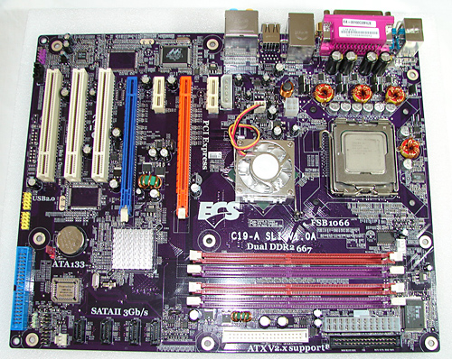
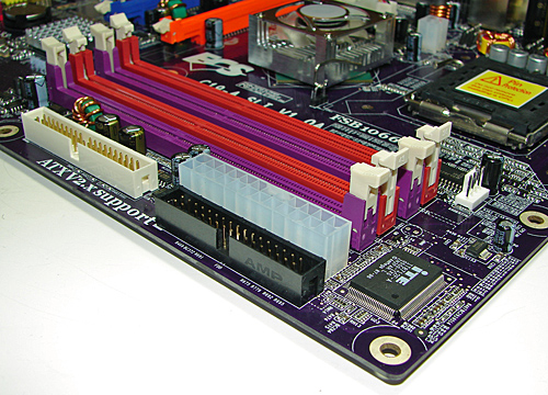
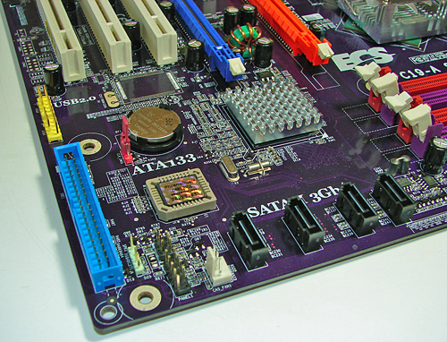
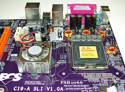
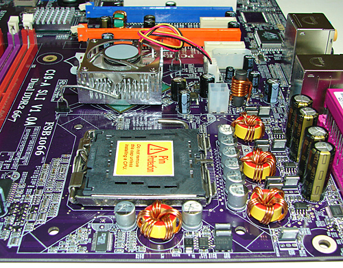
The blue primary NVIDIA nForce4 IDE port connector is located on the left edge of the board and did not present any connection issues in our mid-size ATX case. The location of this connector is very good for most cases and those users still utilizing IDE hard drives. The chassis panel and fan header is located between the primary IDE connector and the nForce4 SATA ports. The BIOS chip is located directly above the chassis panel and fan header.
The yellow NVIDIA nForce4 USB connectors are located above the primary IDE connector and along the edge of the board. The battery and CMOS jumper block is located above the BIOS and to the left of the MCP chipset. The clear CMOS jumper block is a traditional jumper design and is easily accessed.
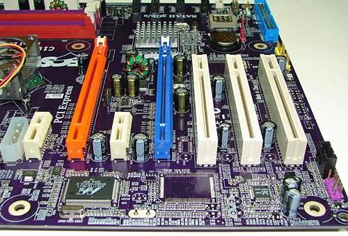
The first PCI Express x1 connector is located to the right of the 4-pin 12V connector. This 4-pin 12V connector is required for dual graphic card or SLI operation. The location of this PCI Express x1 connector allows installation of most peripheral PCI Express cards and is not blocked by most video card designs.
The first physical x16 connector (orange) is located next, followed by the second PCI Express x1 connector. When utilizing a dual slot video card, this PCI Express x1 connector will be physically rendered useless. We did not have any issues utilizing this slot with video cards containing single slot cooling systems.
The second physical x16 connector (blue) is located next, followed by the three PCI 2.3 compliant 32-bit connectors. When utilizing a dual slot video card, the first PCI connector will be rendered physically useless. There were no issues utilizing this slot with video cards containing single slot cooling systems.
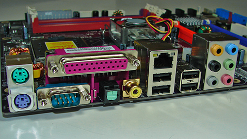
The Marvell 88E1115 Gigabit Ethernet LAN PHY is located in front of the first x16 connector. The Realtek ALC-883 HD audio codec is located in front of the number two PCI connector. The front panel audio header is color-coded purple and located at the edge of the board with the black analog audio input connector situated behind it.
The NVIDIA nForce4 SLI XE SPP chipset is actively cooled with a large heat sink/fan unit that did not interfere with any installed peripherals. Our only concern is the lifespan of the fan and it does generate a slight whirling sound during operation.
The blue primary NVIDIA nForce4 IDE port connector is located on the left edge of the board and did not present any connection issues in our mid-size ATX case. The location of this connector is very good for most cases and those users still utilizing IDE hard drives. The chassis panel and fan header is located between the primary IDE connector and the nForce4 SATA ports. The BIOS chip is located directly above the chassis panel and fan header.
The yellow NVIDIA nForce4 USB connectors are located above the primary IDE connector and along the edge of the board. The battery and CMOS jumper block is located above the BIOS and to the left of the MCP chipset. The clear CMOS jumper block is a traditional jumper design and is easily accessed.
The first PCI Express x1 connector is located to the right of the 4-pin 12V connector. This 4-pin 12V connector is required for dual graphic card or SLI operation. The location of this PCI Express x1 connector allows installation of most peripheral PCI Express cards and is not blocked by most video card designs.
The first physical x16 connector (orange) is located next, followed by the second PCI Express x1 connector. When utilizing a dual slot video card, this PCI Express x1 connector will be physically rendered useless. We did not have any issues utilizing this slot with video cards containing single slot cooling systems.
The second physical x16 connector (blue) is located next, followed by the three PCI 2.3 compliant 32-bit connectors. When utilizing a dual slot video card, the first PCI connector will be rendered physically useless. There were no issues utilizing this slot with video cards containing single slot cooling systems.
The Marvell 88E1115 Gigabit Ethernet LAN PHY is located in front of the first x16 connector. The Realtek ALC-883 HD audio codec is located in front of the number two PCI connector. The front panel audio header is color-coded purple and located at the edge of the board with the black analog audio input connector situated behind it.
The NVIDIA nForce4 SLI XE SPP chipset is actively cooled with a large heat sink/fan unit that did not interfere with any installed peripherals. Our only concern is the lifespan of the fan and it does generate a slight whirling sound during operation.


12 Comments
View All Comments
mindless1 - Saturday, March 25, 2006 - link
Well, you could just tell us. Previously ECS used a lot of OST caps but these may be Panasonic FM? (at least some, the 10mm x 25(?)mm look like it in the VRM. More significant might be the lack of capacitors for memory, could be part of why the board is a bit fickle about o'c.Per Hansson - Saturday, March 25, 2006 - link
Sounds very good Gary ;-)