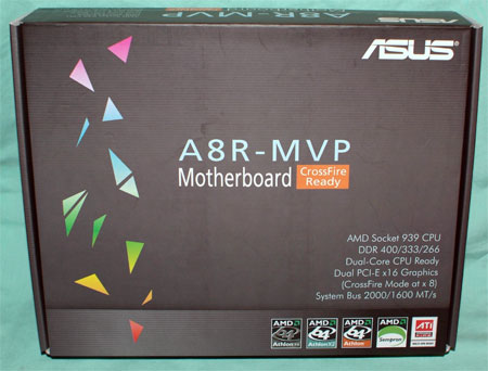
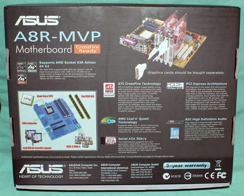
Asus A8R-MVP: Mainstream Rocket
by Wesley Fink on November 23, 2005 1:15 AM EST- Posted in
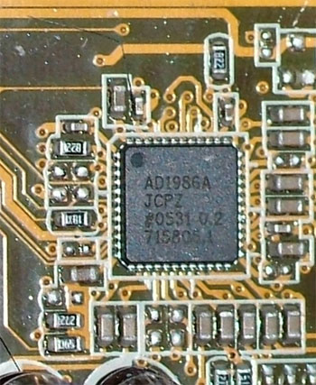
- Motherboards
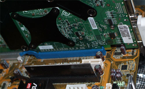
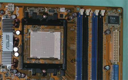
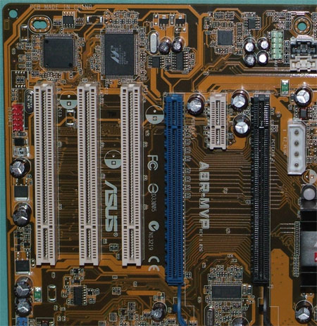
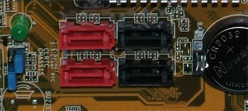
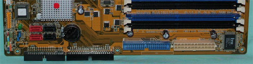
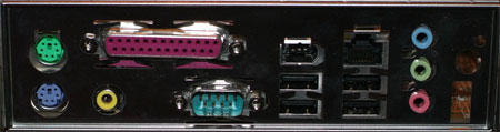
Asus A8R-MVP: Board Layout
Click to enlarge.
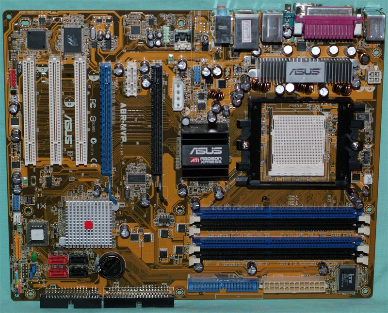
Click to enlarge.


74 Comments
View All Comments
poohbear - Thursday, November 24, 2005 - link
thanks for clarifying.:) guess it's best to wait and see other reveiws to get a general consensus though.Calin - Wednesday, November 23, 2005 - link
Maybe the design team had a set of design cues for the board, received from the top (management) - these include cost, performance, reliability, and possibly even other metrics. The ATI chipset might have been too good for those cues, or maybe they worked to optimize the board - and told nothing to management about their substantial successes.Or maybe the board was a lucky one, and maybe 1 in 100 will get near those results, and the rest will be mainstream. Anyway, I think it is a good design, and not a lucky board
Calin
poohbear - Wednesday, November 23, 2005 - link
jesus 2900mhz on air?!!?? i LOVE competition.:)CrystalBay - Wednesday, November 23, 2005 - link
Hi Wes, Did you run into any coldboot problems ?Wesley Fink - Wednesday, November 23, 2005 - link
No Coldboot problems at working overclocks. We did find, however, that failed overclocks at very high frequencies usually required the system be turned off (power switched off) for the board to recover from the failed OC. This is common to many motherboards, but it is always easier if the board recovers on a warm boot.Diasper - Wednesday, November 23, 2005 - link
Just wondering why there weren't any game benchmark comparisons against the Asus A8N32 given the article set out by comparing them and given the numerous benchmarks with it including Aquamark, how come it was excluded from the rest of the game benchmarks?? It would be pretty nice/important if you included them.nvidia4ever - Wednesday, November 23, 2005 - link
I was wondering the same. Either the results are not favorable for ATI or there are results coming that were not posted yet. Either way it looks like a great board.Wesley Fink - Wednesday, November 23, 2005 - link
The original benchmarks with the A8N32-SLI Deluxe were run at 1600x1200 with AA/AF on. This is because we were trying to determine if Dual x16 SLI made any difference compared to Dual x8 SLI. When we tested the ATI we reran benchmarks on one of the current top nForce4 boards - the DFI LANParty nForce4 SLI - to provide a comparison with the nForce4 SLI chipset. We did not have the Asus A8N32-SLI available for retesting since another reviewer was using the board for benchmarking. It also didn't seem important to also rerun benches on the A8N32-SLI since its performance was comparable to the DFI nF4 SLI.At any rate, the A8N32-SLI is available again and we will rerun some benches at 1280x1024 and add results to the game graphs. For "Standard Score" benchmarks like 3DMarks and Aquamark 3 the video resolutions are always the same and the A8N32-SLI results are already included in the graphs.
Beenthere - Wednesday, November 23, 2005 - link
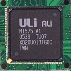
It was pretty obvious a year ago that ATI had created a very impressive chipset for the AMD Mobos. The Southbridge ULi chip resolves perceived deficiencies by those who believe they need faster USB and S-ATA 2, even though in reality this simply isn't true. The fact that the ATI Northbridge chipset O/C's so well is proof of an excellent design and one to build a Helleva reputation on in the Mobo market. The ATI chipset makes it pretty obvious that you don't need to endure high prices and marketing gimmicks of some Mobo mfgs. to promote over-priced "gamers or overclockers" Mobos that don't deliver as much, let alone more PC performance than the ATI chipset Mobos, which include all the practical overclocking BIOS options anyone would possibly need.sunshine - Wednesday, November 23, 2005 - link
RE: "Our first efforts at overclocking the A8R-MVP ran into a road block at just over 260. We have found some Asus boards in the past that did not like overclocks to be immediately set to high values, so we started again at 250. By going up just 5 to 10FSB at a time, we were able to reach 325."What is it exactly that prevents you from setting up the overclocking settings all at once? Why must you increase at only 5 - 10 mhz at a time? Is the Asus Bios boobytrapped to prevent someone from frying their motherboard or CPU???