Intel's Process Roadmap to 2025: with 4nm, 3nm, 20A and 18A?!
by Dr. Ian Cutress on July 26, 2021 5:00 PM ESTCustomers Customers Customers
As a roadmap announcement today, the focus isn’t so much on the customers but on the technology. Because Intel is moving into a phase where it expects its IFS offerings to compete against the established players, it has to consider its disclosures with respect to both its internal use and any external interest, which is a new concept for the company – at least on this scale compared to its previous foundry efforts.
Intel CEO Pat Gelsinger, in the company’s Q3 financial call last week, was keen to point out that they already have a large hyperscaler customer signed up for their next generation packaging technology, however today there would appear to also be another customer in the mix. Now we assume that Intel’s Foundry Services is talking to 100s of chip companies, big and small, but it doesn’t take much to sign an NDA to start to talk – what will be interesting is when customers start making commitments to using Intel’s facilities, and if any of those are volume orders.
As part of the announcement today, Intel held a little bit back from us, saying that they are saving some of the details specifically for the event that is going on as we publish this piece. All we know is that our draft press release has a big yellow bar that says ‘[customer news]’ on it, right next to Intel’s 20A process node details.
For reference, Intel 20A is a 2024 technology using first generation Gate-All-Around transistors, marketed as RibbonFETs, as well as backside power delivery, marketed as PowerVias. At this time Intel expects to have second/third-generation EMIB available as well as fourth-generation Foveros Direct. So if a customer is already committing to Intel 20A, there’s going to be a lot of potential here.
When the announcement is made, we will update this news article.
To conclude, Intel maintains that these roadmaps will showcase a clear path to process performance leadership* by 2025. It’s a tall order, and the company has to execute better than it has in recent memory - but that’s kind of why the company has rehired a number of former Intel experts and fellows in research, product design, and execution.
*as measured by performance per watt at iso-power
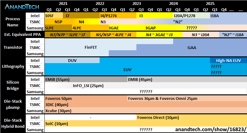
Here's a secondary comparison chart (compared to the one on page one) with all three main foundry offerings listed in each of the main segments that Intel has discussed today.


326 Comments
View All Comments
Maksdampf - Tuesday, July 27, 2021 - link
You know that Intels numbers that they out out haven't been spotted in the wild on any of their products, right? They had been doing these marketing stunts for a while, just with a different disguise. 107MTr/mm2 vor 10SF, my Ass.Since Pat has relased some Transistor count figures, we know that cometlake with 4,2BTr and 205mm2 only has a density of around 21MTr/mm2 instead of the claimed 44MTr/mm2 for 14nm++ and even the newest shiniest rocketlake is worse than AMDs original zeppelin design in Density (6BTr on 270mm2 vs 4.8BTr on 192mm2).
Since Tigerlake-H is only different in its L3 cache system, we know it is around 8-9BTr compared to cypress cove based Rocketlake. And it still has the much larger DIE coming in at 190mm2 compared to AMDs Cezanne with 10,78BTr including a much beefier GPU.
And this is comparing Apples to Apples, so HP processes to HP, not High density to mobile.
TSMCs and Samsungs Mobile Processes are in reality so far ahead in Density and Power of anything Intel ships, that you really need an M1 class of chip to show it.
Intel has us fooled by meaningless laboratory numbers that can nowhere be found in real products for years and now they fuck us over again by renaming those already pretty desperate naming schemes.
name99 - Tuesday, July 27, 2021 - link
Not if those transistor estimates never match real products…For years now, nothing Intel ships is close to their claimed transistor density. It’s like 2 to 3x off.
So…
Butterfish - Tuesday, July 27, 2021 - link
So does most chip made by other foundries. These figure are for the high density library. If you look at AMD’s CPU and GPU which use TSMC’s high performance library that aren’t optimized for density you will see much lower density number compare to what was advertised for the process nodes they are using.Spunjji - Wednesday, July 28, 2021 - link
Yes, you will see lower density - but something like 60-80% of the quoted density. Intel are hitting something more like 33-50% of what they quoted for 10nm.cheshirster - Tuesday, July 27, 2021 - link
Intel hide transistor density of their products since Coffee Lake.For years as of now.
cheshirster - Tuesday, November 23, 2021 - link
Still Intel, cause their transistors counts aren't disclosed for any 10nm product.IntelUser2000 - Monday, July 26, 2021 - link
No, Ian lobbied for it.Boo!!
mode_13h - Tuesday, July 27, 2021 - link
Yeah, as a journalist, he shouldn't be trying to influence the industry. He can ask them questions like how they feel about TSMC/Samsung's node naming, during interviews, but that about as far as it should go.Oxford Guy - Wednesday, July 28, 2021 - link
I can only assume your post is not particularly well-executed parody of the misguided point of view it’s espousing.What a stupid comment.
Journalists, of course, can (and often should) be more than marketing department parrots, more than stenographers.
Spunjji - Thursday, July 29, 2021 - link
I'm always confused by that idea that there's some magical bright line between being a journalist and an enthusiast. Ian can advocate for whatever he wants from Intel - as long as he's actually honest about it, IDGAF.