Intel's Process Roadmap to 2025: with 4nm, 3nm, 20A and 18A?!
by Dr. Ian Cutress on July 26, 2021 5:00 PM ESTCustomers Customers Customers
As a roadmap announcement today, the focus isn’t so much on the customers but on the technology. Because Intel is moving into a phase where it expects its IFS offerings to compete against the established players, it has to consider its disclosures with respect to both its internal use and any external interest, which is a new concept for the company – at least on this scale compared to its previous foundry efforts.
Intel CEO Pat Gelsinger, in the company’s Q3 financial call last week, was keen to point out that they already have a large hyperscaler customer signed up for their next generation packaging technology, however today there would appear to also be another customer in the mix. Now we assume that Intel’s Foundry Services is talking to 100s of chip companies, big and small, but it doesn’t take much to sign an NDA to start to talk – what will be interesting is when customers start making commitments to using Intel’s facilities, and if any of those are volume orders.
As part of the announcement today, Intel held a little bit back from us, saying that they are saving some of the details specifically for the event that is going on as we publish this piece. All we know is that our draft press release has a big yellow bar that says ‘[customer news]’ on it, right next to Intel’s 20A process node details.
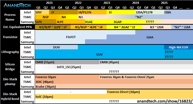
For reference, Intel 20A is a 2024 technology using first generation Gate-All-Around transistors, marketed as RibbonFETs, as well as backside power delivery, marketed as PowerVias. At this time Intel expects to have second/third-generation EMIB available as well as fourth-generation Foveros Direct. So if a customer is already committing to Intel 20A, there’s going to be a lot of potential here.
When the announcement is made, we will update this news article.
To conclude, Intel maintains that these roadmaps will showcase a clear path to process performance leadership* by 2025. It’s a tall order, and the company has to execute better than it has in recent memory - but that’s kind of why the company has rehired a number of former Intel experts and fellows in research, product design, and execution.
*as measured by performance per watt at iso-power
Here's a secondary comparison chart (compared to the one on page one) with all three main foundry offerings listed in each of the main segments that Intel has discussed today.


326 Comments
View All Comments
bigboxes - Tuesday, July 27, 2021 - link
Yeah, Intel is still king of the liars. I've got a box full of Intel CPUs, but Intel really crapped the bed. Intel 7 is the new 10nm. Can't make this stuff up! We can't put out a competitive product so we'll call it 7 anyways! GO INTEL GO!Geef - Saturday, July 31, 2021 - link
At least Intel is consistent. They have consistently added a + to their 14nm chips every single year!mode_13h - Sunday, August 1, 2021 - link
:Daovander - Tuesday, August 3, 2021 - link
Which is exactly what TSMC did with their 14nm node.This was how the whole naming problem got started but no one seemed to care since it seemed like they were catching up to Intel and all the Intel haters were happy to see it.
When Intel shocked the world and released its FinFET (Tri-Gate) process at 22nm TSMC followed it with the horrible 20nm planar node though it had lower transistor density than Intel 22nm. TSMC was claiming its 20nm node was a half shrink of the 22nm node and therefore meant they were keeping up with Intel. TSMC felt they were justified in this because Intel 22nm transistor density missed the target of a full node shrink by a bit with the introduction FinFET's. This was a consequence of the new trench contact structure required between the Fin’s and Metal 0. TSMC has the same problem when they introduce Fin’s. Then, Intel released 2nd Gen FinFET, the 14nm node, with more than a full node of shrinkage to get back on track with what they missed at 22nm.
TSMC then released their 14nm node shortly after with the same backend as the 20nm node - so no transistor density scaling, it was the same node really (sound familiar). Then, Intel got over-optimistic and tried to scale more than a full node again using Spacer Quad patterning at 10nm and got stuck in a 6 year delay. At the same time they decided to pass on using EUV for 10nm because at the time it was not ready for production.
TSMC bought up all the EUV steppers in the world and then proceeded down the lithographic scaling trail of 10nm, 7nm, 5nm, and soon 3nm. A smart move on their part and easier to make since the throughput of the EUV tool increased in the meantime (since they were a bit behind Intel in that development decision). Essentially all this scaling was handed to them on a silver platter by ASML. Also, the transistor density of these 3-4 nodes has been well off the traditional density shrink which is why Intel 2 nodes (or more depending on how you interpret the marketing names) still has a density that matches them.
They did not produce any real innovations in any of those nodes. Gate-all-around has been the obvious next step for 5-6 years. If they were "innovating" all this time with all these new nodes why did they not develop this. Now we see everyone claiming to have it ready to go in the 2024-2025 timeframe since IBM made their 2nm announcement. Funny how that is, wonder where everyone is getting it from?
All I am saying is, if you are going to call Intel a Liar then you have to call everyone else one first.
Given the confusion in the industry and the desire to truly compare technologies names with matched Transistor density, the whole world pushed Intel into changing their naming scheme since there was no possibility of getting the foundries to go backwards.
mode_13h - Wednesday, August 4, 2021 - link
@aovander thanks for the info.As I've said several times, Intel can just name their node with a monotonically increasing sequence that has no obvious or direct relation to density. Just opt out of the whole nm race, entirely.
Dex4Sure - Tuesday, November 23, 2021 - link
Intel's 10nm is actually slightly better than TSMC's 7nm in density... So they may as well call it "Intel 7".Butterfish - Tuesday, July 27, 2021 - link
Any proof? Or just pulling thin air out of your arse to satisfy your agenda? The density comparison graph in the first page of this article literally disapprove your statement.Spunjji - Wednesday, July 28, 2021 - link
@Butterfish - not to agree with DigitalFreak here, but it's worth noting that Intel haven't actually managed to produce a shipping design anywhere near their quoted density for 10nm, while TSMC customers (most notably AMD) have come much closer to their quoted density.I'd still say that 10ESF looks broadly comparable to TSMC 7nm, though - much moreso than Samsung's 8nm.
Butterfish - Thursday, July 29, 2021 - link
Yes they have. The Cannon Lake Core i3-8121U did use the high density libraries that has the advertised maximum density for 10nm.Spunjji - Friday, July 30, 2021 - link
@Butterfish - You're citing the broken chip that only shipped in one cut-price notebook; one that doesn't have public figures for transistor count available, so we don't know anything for sure about the density. The possibilities are either that you're technically correct in the worst way - i.e. they haven't shipped anything that /worked properly/ with their quoted 100M density - or you're wrong on both counts. 🤷♂️Back in the world of numbers we know for sure, Lakefield hit almost exactly 49% of their quoted 10nm density, and that had all the inconvenient I/O stuff shunted off to its secondary die.