Intel's Architecture Day 2018: The Future of Core, Intel GPUs, 10nm, and Hybrid x86
by Dr. Ian Cutress on December 12, 2018 9:00 AM EST- Posted in
- CPUs
- Memory
- Intel
- GPUs
- DRAM
- Architecture
- Microarchitecture
- Xe
Changing How Chips are Made: 3D Packaging with FOVEROS
Anyone who has followed any amount of chip design in semiconductors should well-aware that most of the CPUs and SoCs in production today are based on monolithic dies – single pieces of silicon the have all what is needed inside, before being placed on a package and into a system. While rarer, there are multi-chip packages, were multiple chips go in one package with a shared connection. Beyond this we have seen interposers or embedded bridges designed to bring different chips together with high-speed interconnects. Now Intel is ready to bring 3D stacking into the mass market.
One of the biggest challenges in modern chip design is minimizing die area. A small die decreases costs – typically power too – and can make it easier to implement in a system. When it comes down to extracting performance however, we are at the limits of scale – one of the downsides of big monolithic dies, or even multi-chip packages, is that memory is too far away. Intel today is now ready to talk about its Foveros technology, which involves active interposers in small form factors to bring differentiated technologies together.
Foveros: It’s Greek for Awesome, Apparently
The way Raja introduced this technology started with discussing process technologies. Intel has for many years/decades been focused on high performance process nodes, trying to extract as much as possible from its high-performance cores. Alongside this, Intel also runs an IO optimized process node on a similar cadence but more suitable for PCH or SoC-type functions.
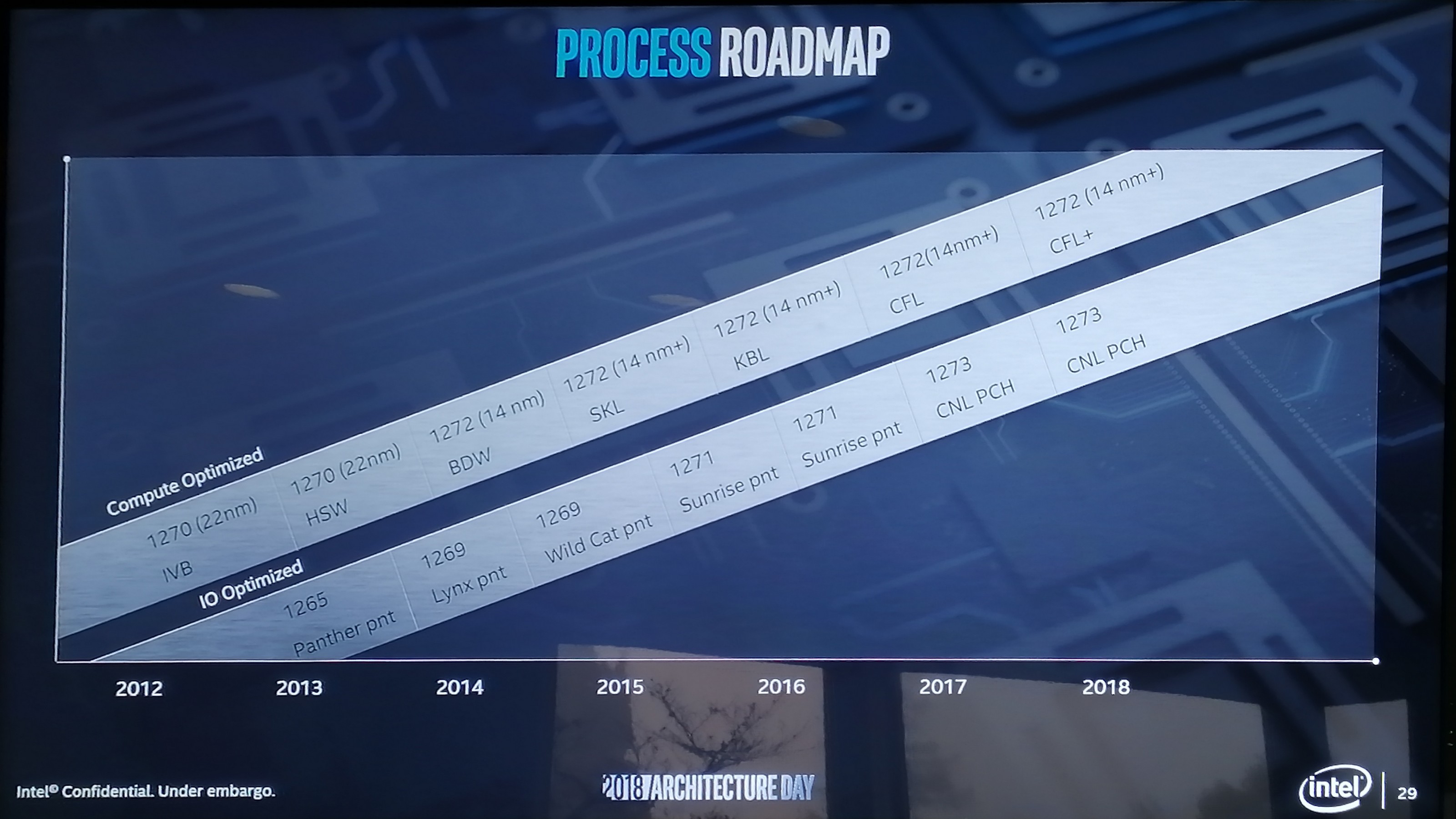
The 126x and 127x are the internal numbering systems for Intel’s process node technologies, although they don’t differentiate between BKM updates for the "+" node variants it turns out. But the point here is that Intel already knows that it needs certain process optimizations in place depending on the type of transistors, performance, and power needed. Going forward, Intel is going to be expanding its node base out so it can cover more power and performance points.
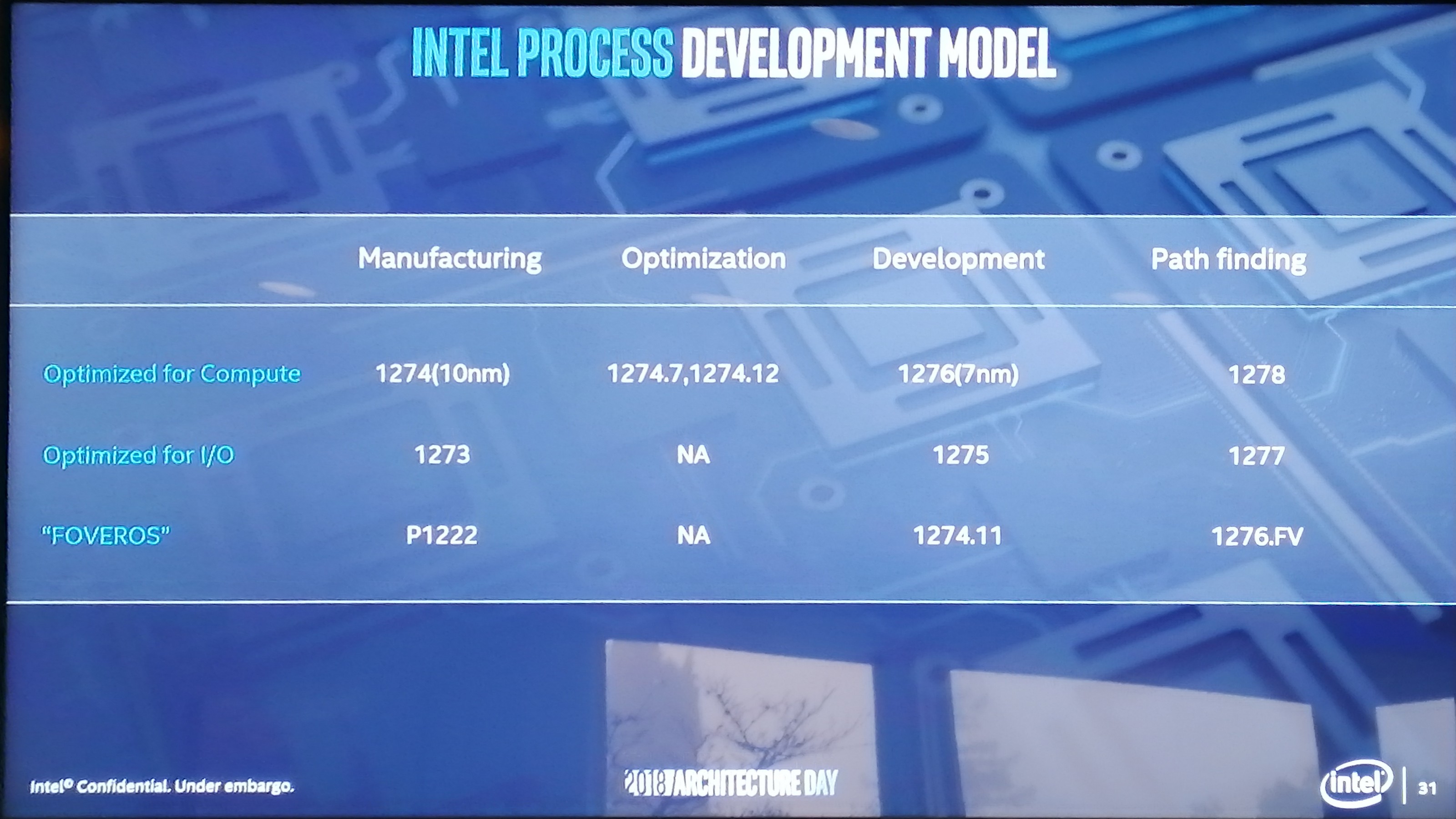
So for this example, Raja pulled out the current set of process technologies for 2019. For a manufacturing process, compute has the 1274 process on 10nm, IO has the 1273 process (14nm), while this new special Foveros technology is under P1222. Alongside the manufacturing, Intel will be working on optimizations focusing on the compute aspects of the manufacturing node. There will also be a set of developments for future node technologies, and the final column shows that Intel has path-finding research to look into future technologies and determine what capabilities will be possible on future designs. This sounds pretty much what a company like Intel should be doing, so no argument from me so far. The goal here is that each type of transistor use case can be different, and there isn’t a one-size fits all approach.

One way to assist with this is through chiplets and packaging. By picking the best transistor for the job in each case, whether it is CPU, GPU, IO, FPGA, RF, or anything else, with the correct packaging, it can be put together to get the best optimizations available.
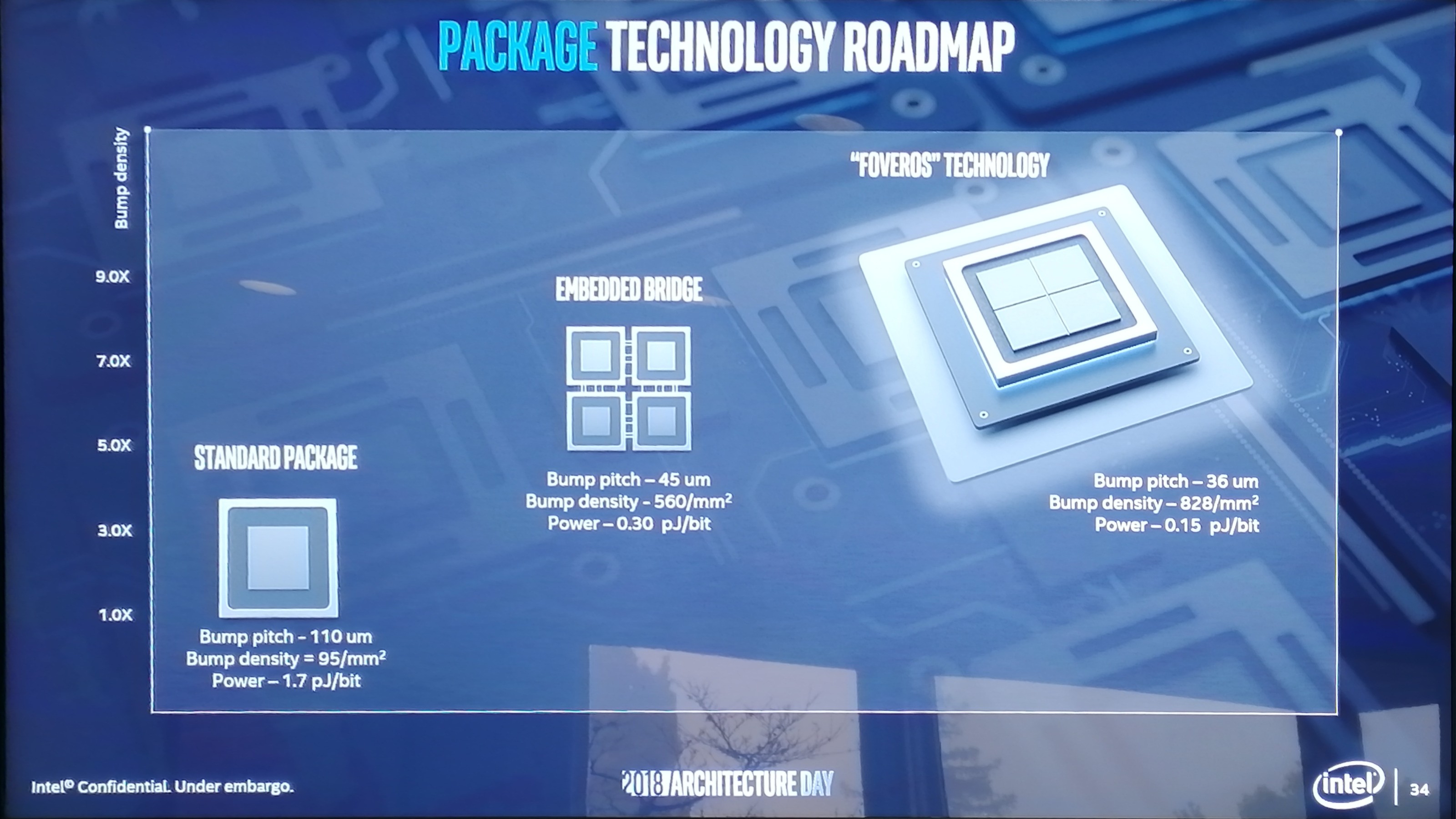
So here’s where Foveros fits in. Foveros is Intel’s new active interposer technology designed as a step above its own EMIB designs for small form-factor implementations, or those with extreme memory bandwidth requirements. For these designs the power per bit of data transferred is super low, however the packaging technology has to deal with the decreased bump pitch, the increased bump density, and also the chip stacking technology. Intel says that Foveros is ready for prime time, and they can produce it at scale.
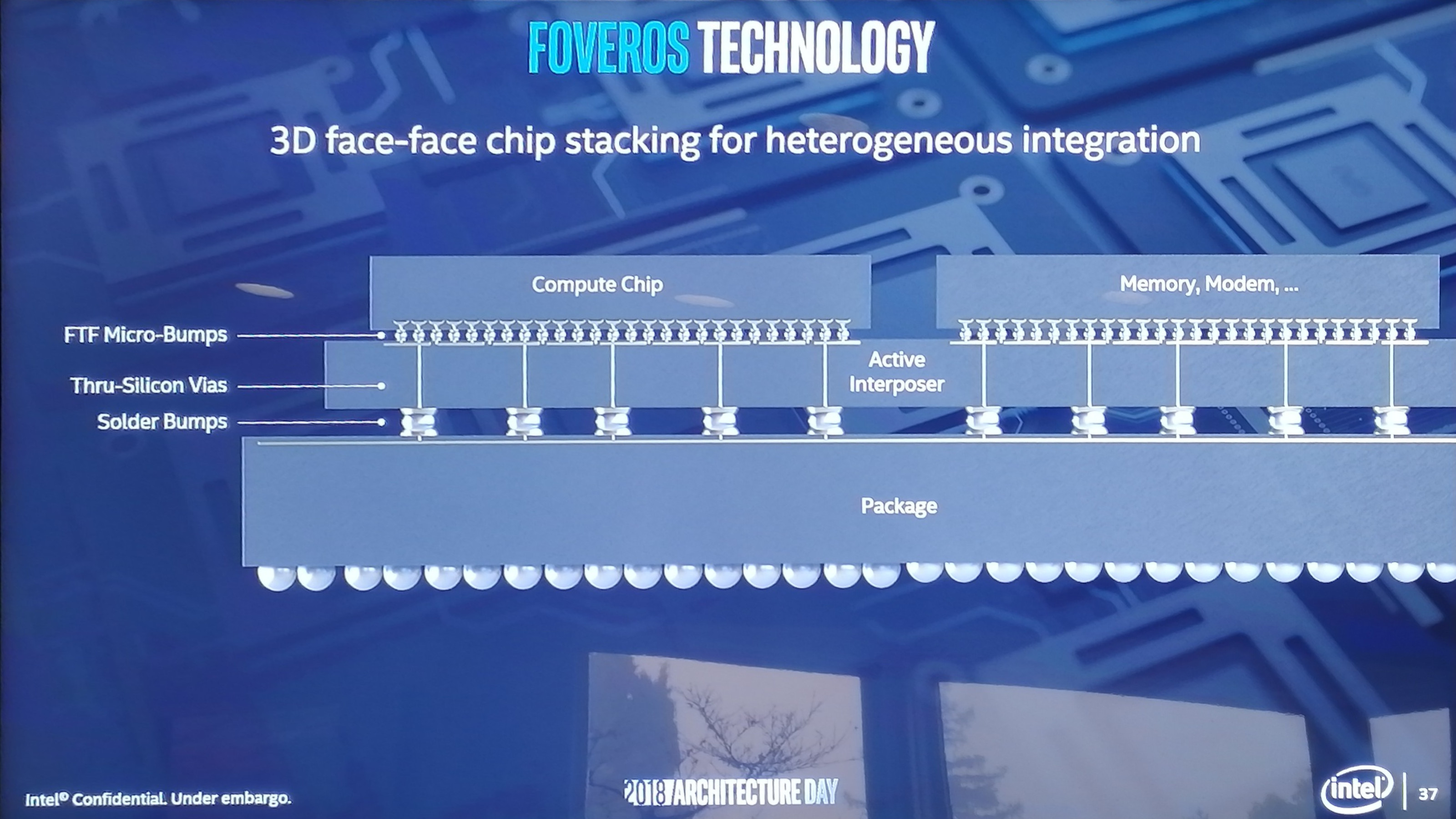
So this Foveros ‘3D’ packaging just sounds like a silicon interposer, such as what we’ve seen on AMD’s Fiji or NVIDIA’s high-end datacenter GPUs. However Intel is going above what those products are doing by actually making the interposer part of the design. The interposer contains the through-silicon vias and traces required to bring power and data to the chips on top, but the interposer also carries the PCH or IO of the platform. It is, in effect, a fully working PCH, but with vias to allow chips to be connected on top.
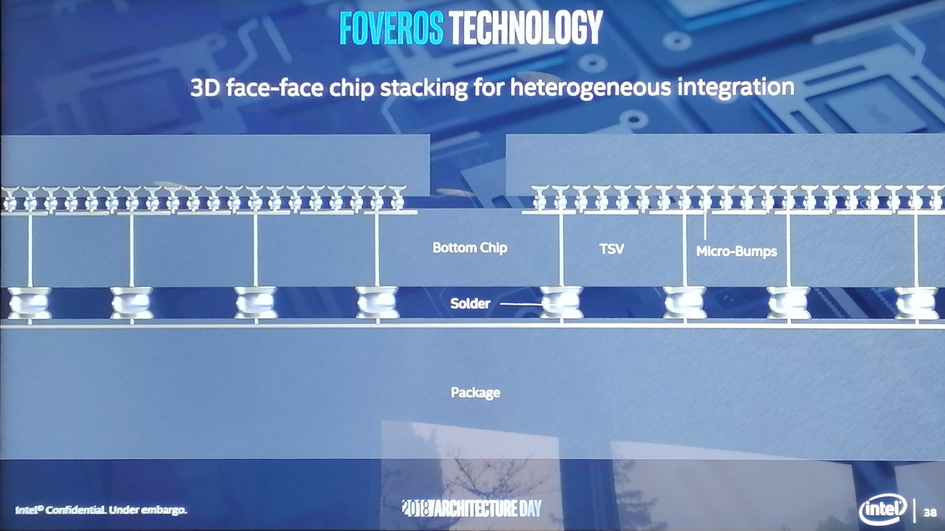
The first iteration of this technology is less complicated that the slide above, just using a set of CPU cores attached to the PCH below, but the idea is that a large interposer can have select functions on it and those can be removed from the chips above to save space. This also lets Intel use the different transistor types in different chips – the example we were given uses an interposer built on the 22FFL process node, with a 10nm set of CPUs on the top die. Above this, DRAM is provided in a POP package. Sounds cool, right?
In actual fact, Intel had a Foveros chip or two working in the demo area. These, Intel explained, were hybrid x86 designs that combined a single big Core with four smaller Atom cores on the same 10nm piece of silicon. I’m sure I’ve heard about big.Little before, but I was shocked that Intel is actually going to do it! We managed to take a photo of the block diagram, which Intel removed from its slide deck before sending it out to the press after the presentations. All details on the next page.


148 Comments
View All Comments
peevee - Tuesday, December 18, 2018 - link
"Normally cache misses decrease by a factor of a square root of the proportional size when the cache is increased"This is neither true in most performance-critical real cases nor can provide any estimate of actual performance increase.
mikato - Friday, December 21, 2018 - link
I'm here for the "raja inside" comments. Disappointed.peevee - Sunday, December 23, 2018 - link
"although it was pointed out that these improvements won’t help everyone, and might require new algorithms in order to use specific parts of the core."Which means it will help almost no one, as very few will optimize specifically for that core.
"We’re waiting to see what changes Intel has made on the front-end, which is where a lot of low-hanging fruit often lies for performance."
Low-hanging fruit in x86 was picked up in Pentium. Since then it is just more and more kludges which cost more energy than improve performance (normalizing for node).
peevee - Sunday, December 23, 2018 - link
"64 EUs... Each EU will support seven threads as before, which means that the entire GT2 design will essentially have 512 concurrent pipelines."Math?
And are these threads? Or ALUs?
peevee - Sunday, December 23, 2018 - link
"The 7-Zip demo was relatively straight forward, showing how the new instructions such as Vector-AES and SHA-NI in Sunny Cove can give the processor a 75% boost in performance over an equivalent Skylake based platform at iso-frequency."Huh? Have they recompiled (what compiler supports the new instructions then), or manually wrote a codepath in asm? And enabled encryption so to get any increase, so the increase is not actually for compression? Have they disabled compression too? ;)
dampf - Wednesday, January 2, 2019 - link
Really Intel? Adding AI improvements to Core architecture in 2021? Smartphone vendors were doing it last year... way too late. And 5G will take off in the end of 2019.TheJian - Wednesday, January 2, 2019 - link
I guess I'm not getting why I should be impressed by this.https://www.electronicsweekly.com/news/design/comm...
Leti already did it? They say it's IP can be used by others, so is this Intel's solution (what they're using I mean)?
AMD already does chiplets, everyone does socs (Intel failed them)...etc. 144mm^2 not that small (about an large apple soc size). Current 7nm A12 is 83mm^2 with 6.9B transistors and two big cores, 4 small. AMD already did interposer/chiplets. Memory has been stacking for a while now. Not sure what is supposed to impress me here.
"Very much like a mobile chip" ...Pretty much...Again, why so impressed?
And as OP noted, you have no idea how big the market is, nor how much they can make on them. I think they have to try to sell some before we can say that (many Intel things killed over the years), as their last mobile strategy cost them 16B+ in giveaways, and lost the fab race for a while (maybe forever, because that 16B lost should have went DIRECTLY into fabs and 10nm wouldn't be crap now), as once 7nm Intel hits, it looks like TSMC beats them anyway with 5nm (ok, tie? whatever). My point here is Intel's 7nm won't be much ahead of tsmc 5nm if at all as that is what it will compete with since tapeouts happen q2 2019 and chips 12-15 months later.
https://www.extremetech.com/computing/278742-tsmc-...
Many other articles out there like this, but has a good chart of when and how much wafers etc. But if risk production is really as they say, 5nm chips by xmas 2020. That puts Intel where with this @7nm? Unless that answer is XMAS 2020, I'm thinking behind tsmc. It looks like TSMC is aiming before xmas and they've been moving at a good clip without many glitches recently, so Intel better get busy IMHO. TSMC is 2q 2019 risk, or 2H 2019 depending on who you believe I guess. But still, Intel 7nm better hit by xmas 2020 then right?
Comments on last page: Uh, should have bought NV under $10 but couldn't take the best from gpu side because nobody could handle Jen as president :) WOW, look at that value you passed up Intel, oh, and you'd RULE mobile by now with all those tegras being on Intel's process 5+yrs ago (never mind what gpus would have done on Intel during this time) and you already had the modem solution too (NV bought one, and had to kill it, intel would have taken over everything cpu/gpu/modem/mobile).
With chromebooks, 2b mobile units not using NV gpu's etc, nobody would have stopped them at FTC since more gpus, and arguably more computing devices ship without WINTEL, Intel's gpus (even with NV in there) etc. Intel gpus wouldn't have been needed, mobile wouldn't have been lost (14nm Intel NV socs would have competed well against 20nm everyone else, same story before 14/20, Intel 22nm NV socs vs. 28nm everyone else)., fab money wouldn't have been blown on mobile etc etc. All the problem Intel has now are because they blew 16B on failing instead of BUYING NV for that or a bit more. They had a value back then ~6B or less 659mil shares at $10, I bought at 12...ROFL. They should have owned NV anywhere in there and all this crap wouldn't have happened...LOL. We'll see how this "ideas from outside" crap works out now. To be fair AMD had the same problems to some extent, firing Dirk for not liking mobile/tablet/apu, and wanting a KING first then that cheap crap later. Now they chase king cpu (not gpu yet so far) again...LOL. Yeah, I own AMD stock but still think management is dumb. Can't price anything right, always trying to be a friend or get share which means NOTHING if it doesn't come with MARGIN as a poor man. Sure the rich guy can flood a market, kill enemy sales, but only because he has wads of cash and can wait until he breaks you. Poor company needs NET INCOME for the next gen R&D and to retain people like KELLER etc.
I'm only in AMD stock for the 7nm server stuff, then out likely. Rumor/hype work well in advance of real product at amd (talking stock price here), so you don't likely have to wait for anything other then "shipping soon" or some leaked benchmarks etc. and the price will head to 40+ probably. Just run before that reality hits or brave the waves...LOL. I think AMD will make money, certainly has the server chips to do it, but management just seems to fail at pricing anything to take advantage while they can. Too worried about market, instead of MARGIN for R&D. I'd rather own the 10% that makes most of the money than the 80% that makes crap+a little midrange crap. Apple thinks the same, see their Q reports for ages etc. Own the rich so you can afford to supply the poor. It doesn't work the other way around generally speaking, especially as the little guy. You can't bleed as the poor little guy ;)
TheJian - Wednesday, January 2, 2019 - link
One more point, in case anyone brings it up, A12x 122mm^2 10B transistors. just adds two more big cores IIRC (maybe a few other small changes). Same point though.