ATI Radeon X800 Pro and XT Platinum Edition: R420 Arrives
by Derek Wilson on May 4, 2004 10:28 AM EST- Posted in
- GPUs
The R420 Vertex Pipeline
The point of the vertex pipeline in any GPU is to take geometry data, manipulate it if needed (with either fixed function processes, or a vertex shader program), and project all of the 3D data in a scene to 2 dimensions for display. It is also possible to eliminate unnecessary data from the rendering pipeline to cut out useless work (via view volume clipping and backface culling). After the vertex engine is done processing the geometry, all the 2D projected data is sent to the pixel engine for further processing (like texturing and fragment shading).
The vertex engine of R420 includes 6 total vertex pipelines (R3xx has four). This gives R420 a 50% per clock increase in peak vertex shader power per clock cycle.
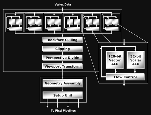
Looking inside an individual vertex pipeline, not much has changed from R3xx. The vertex pipeline is laid out exactly the same, including a 128bit vector math unit, and a 32bit scalar math unit. The major upgrade R420 has had from R3xx is that it is now able to compute a SINCOS instruction in one clock cycle. Before now, if a developer requested the sine or cosine of a number in a vertex shader program, R3xx would actually compute a taylor series approximation of the answer (which takes longer to complete). The adoption of a single cycle SINCOS instruction by ATI is a very smart move, as trigonometric computations are useful in implementing functionality and effects attractive to developers. As an example, developers could manipulate the vertices of a surface with SINCOS in order to add ripples and waves (such as those seen in bodies of water). Sine and cosine computations are also useful in more basic geometric manipulation. Overall, R420 has a welcome addition in single cycle SINCOS computation.
So how does ATI's new vertex pipeline layout compare to NV40? On a major hardware "black box" level, ATI lacks the vertex texture unit featured in NV40 that's required for shader model 3.0's vertex texturing support. Vertex texturing allows developers to easily implement any effect which would benefit from allowing texture data to manipulate geometry (such as displacement mapping). The other major difference between R420 and NV40 is feature set support. As has been widely talked about, NV40 supports Shader Model 3.0 and all the bells and whistles that come along with it. R420's feature set support can be described as an extended version of Shader Model 2.0, offering a few more features above and beyond the R3xx line (including more support of longer shader programs, and more registers).
What all this boils down to is that we are only seeing something that looks like a slight massaging of the hardware from R300 to R420. We would probably see many more changes if we were able too peer deeper under the hood. From a functionality standpoint, it is sometimes hard to see where performance comes from, but (as we will see even more from the pixel pipeline) as graphics hardware evolves into multiple tiny CPUs all laid out in parallel, performance will be effected by factors traditionally only spoken of in CPU analysis and reviews. The total number of internal pipeline stages (rather than our high level functionality driven pipeline), cache latencies, the size of the internal register file, number of instructions in flight, number of cycles an instructions takes to complete, and branch prediction will all come heavily into play in the future. In fact, this review marks the true beginning of where we will be seeing these factors (rather than general functionality and "computing power") determine the performance of a generation of graphics products. But, more on this later.
After leaving the vertex engine portion of R420, data moves into the setup engine. This section of the hardware takes the 2D projected data from the vertex engine, generates triangles and point sprites (particles), and partitions the output for use in the pixel engine. The triangle output is divided up into tiles, each of which are sent to a block of four pixel pipelines (called a quad pipeline by ATI). These tiles are simply square blocks of projected pixel data, and have nothing to do with "tile based rendering" (front to back rendering of small portions of the screen at a time) as was seen in PowerVR's Kyro series of GPUs.
Now we're ready to see what happens on the per-pixel level.


95 Comments
View All Comments
Pumpkinierre - Wednesday, May 5, 2004 - link
Sorry, scrub that last one. I couldnt help it. I will reform.Pumpkinierre - Wednesday, May 5, 2004 - link
So, which is better: a64 at 2Gig or P4 at 3.2?jibbo - Wednesday, May 5, 2004 - link
"Zobar is right; contra Jibbo, the increased flexibility of PS3 means that for many 2.0 shader programs a PS3 version can achieve equivalent results with a lesser performance hit."I think you're both still missing my point. There is nothing that says PS3.0 is faster than PS2.0. You are both correct that it has to potential to be faster, though you both assume that a first generation PS3.0 architecture will perform at the same level as a refined PS2.0 architechture.
PS3.0 is one of the big reasons that nVidia's die size and transistor count are bigger than ATI's. The additional power drain (and consequently heat dissipation) of those 40M transistors also helps to limit the clock speeds of the 6800. When you're talking about ALU ops per second (which dominate math-intensive shaders), these clock speeds become very important. A lot of the 6800's speed for PS3.0 will have to be found in the driver optimizations that will compile these shaders for PS3.0. Left to itself, ATI's raw shader performance still slaughters nVidia's.
They both made trade-offs, and it seems that ATI is banking that PS3.0 won't be a dealbreaker in 2004. Only time will tell....
Phiro - Wednesday, May 5, 2004 - link
K, I found the $400M that the CEO claimed. He also claimed $400M for the NV3x core as well. It seemed more as a boast than anything, not particularly scientific or exact.In any case, ATI supposedly spent $165-180M last year (2003) on R&D, with an estimated increase of 100% for this year. How long has the 4xx core been in development?
Regardless, ultimately we the consumers are the winners. Whether or not the R&D spent pans out will play out over the next couple years, as supposedly the nv4x core has a 24 month lifespan.
413xram - Wednesday, May 5, 2004 - link
If you watch nvidia's launch video on their site they mention the r&d costs for their new card.RyanVM - Wednesday, May 5, 2004 - link
What ever happened to using ePSXe as a video card benchmark?Phiro - Wednesday, May 5, 2004 - link
Well, Nvidia may have spent $400M on this (I've never seen that number before but we'll go with it I guess) but they paid themselves for the most part.ATI's cost can't be too trivialized - didn't they drop a product design or two in favor of getting this out the door instead? And any alteration in the architecture of something doesn't really qualify as a hardware "refresh" in my book - a hardware refresh for an OEM consists of maybe one speed notch increase in the RAM, new bios, larger default HD, stuff like that. MLK is what Dell used to call it - Mid Life Kick.
retrospooty - Wednesday, May 5, 2004 - link
"Precisely. By the time 512mb is useful, the card will be too slow for it to matter, and you'd need a new card any way."True...
Both cards perform great, both have wins and losses depending on the game. The deciding factor will be price and power requirements.
Since prices will adjust downward, at a fairly equal rate, that leaves power. With Power requirements being so incredibly high with the NV40, that leans me toward ATI.
413xram also has a good point above. For Nvidia, this is a 400 million dollar new chip design. For ATI, this was a refresh of an old design to add 16 pipes, and a few other features. After the losses NV took with the heavily flawed NV30 and 35 , they need a financial boom, and this isnt it.
mattsaccount - Wednesday, May 5, 2004 - link
There are no games available today that use 256mb of video RAM, let alone 512mb. Even upper-high-end cards routinely come with 128mb (e.g. Geforce FX 5900, Radeon 9600XT). It would not make financial sense for a game developer to release a game that only a small fraction of the community could run acceptably.>> I have learned from the past that future possibilties of technology in hardware does nothing for me today.
Precisely. By the time 512mb is useful, the card will be too slow for it to matter, and you'd need a new card any way.
413xram - Wednesday, May 5, 2004 - link
#64 Can you explain "gimmick"?