AMD Zen Microarchiture Part 2: Extracting Instruction-Level Parallelism
by Ian Cutress on August 23, 2016 8:45 PM EST- Posted in
- CPUs
- AMD
- x86
- Zen
- Microarchitecture
The Core Complex, Caches, and Fabric
Many core designs often start with an initial low-core-count building block that is repeated across a coherent fabric to generate a large number of cores and the large die. In this case, AMD is using a CPU Complex (CCX) as that building block which consists of four cores and the associated caches.
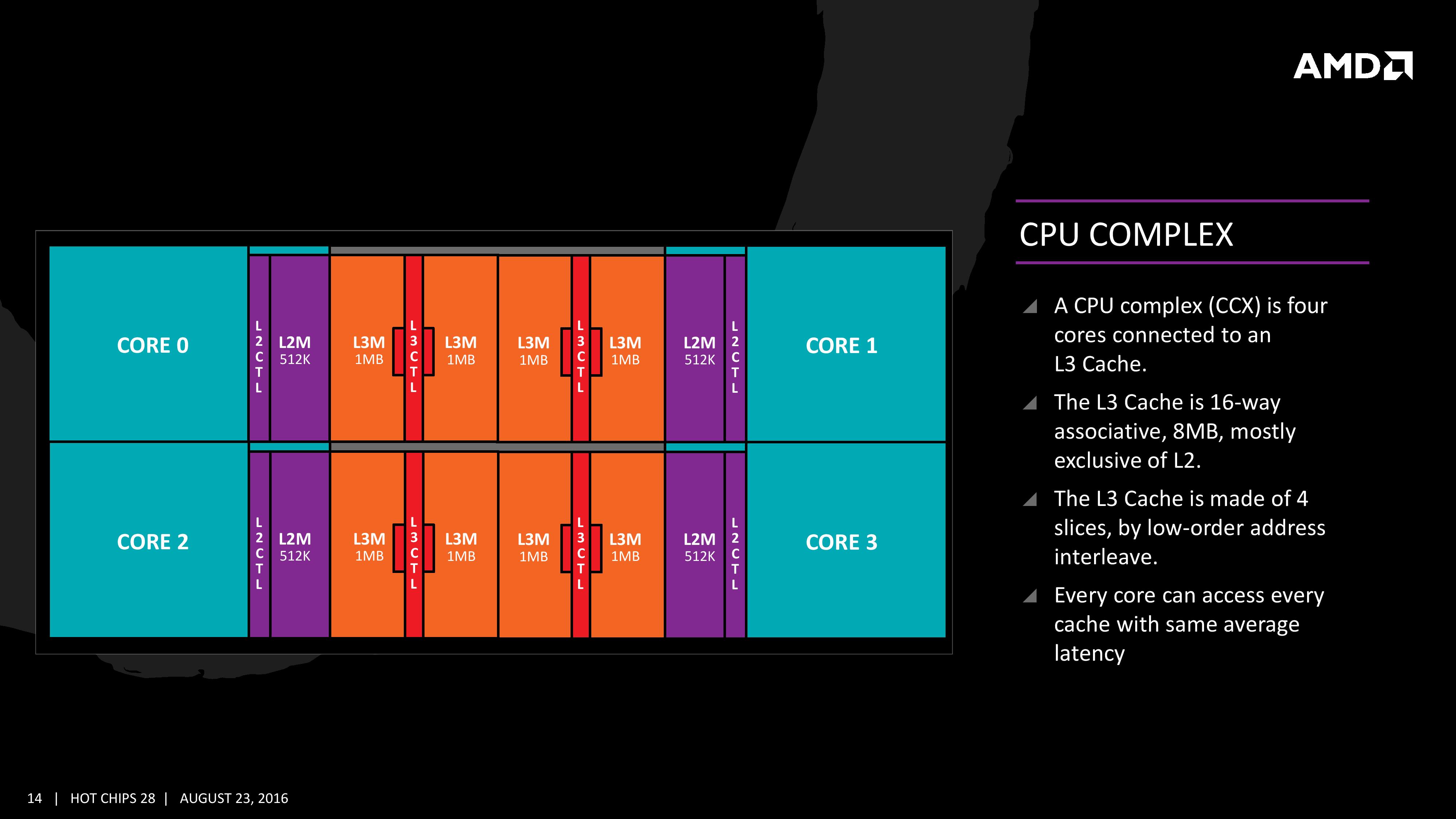
Each core will have direct access to its private L2 cache, and the 8 MB of L3 cache is, despite being split into blocks per core, accessible by every core on the CCX with ‘an average latency’ also L3 hits nearer to the core will have a lower latency due to the low-order address interleave method of address generation.
The L3 cache is actually a victim cache, taking data from L1 and L2 evictions rather than collecting data from prefetch/demand instructions. Victim caches tend to be less effective than inclusive caches, however Zen counters this by having a sufficiency large L2 to compensate. The use of a victim cache means that it does not have to hold L2 data inside, effectively increasing its potential capacity with less data redundancy.
It is worth noting that a single CCX has 8 MB of cache, and as a result the 8-core Zen being displayed by AMD at the current events involves two CPU Complexes. This affords a total of 16 MB of L3 cache, albeit in two distinct parts. This means that the true LLC for the entire chip is actually DRAM, although AMD states that the two CCXes can communicate with each other through the custom fabric which connects both the complexes, the memory controller, the IO, the PCIe lanes etc.
One interesting story is going to be how AMD’s coherent fabric works. For those that follow mobile phone SoCs, we know fabrics and interconnects such as CCI-400 or the CCN family are optimized to take advantage of core clusters along with the rest of the chip. A number of people have speculated that the fabric used in AMD’s new design is based on HyperTransport, however AMD has confirmed that they are not using HyperTransport here for Zen. More information on the fabric may come out as we nearer the launch, although this remains one of the more mysterious elements to the design at this stage.
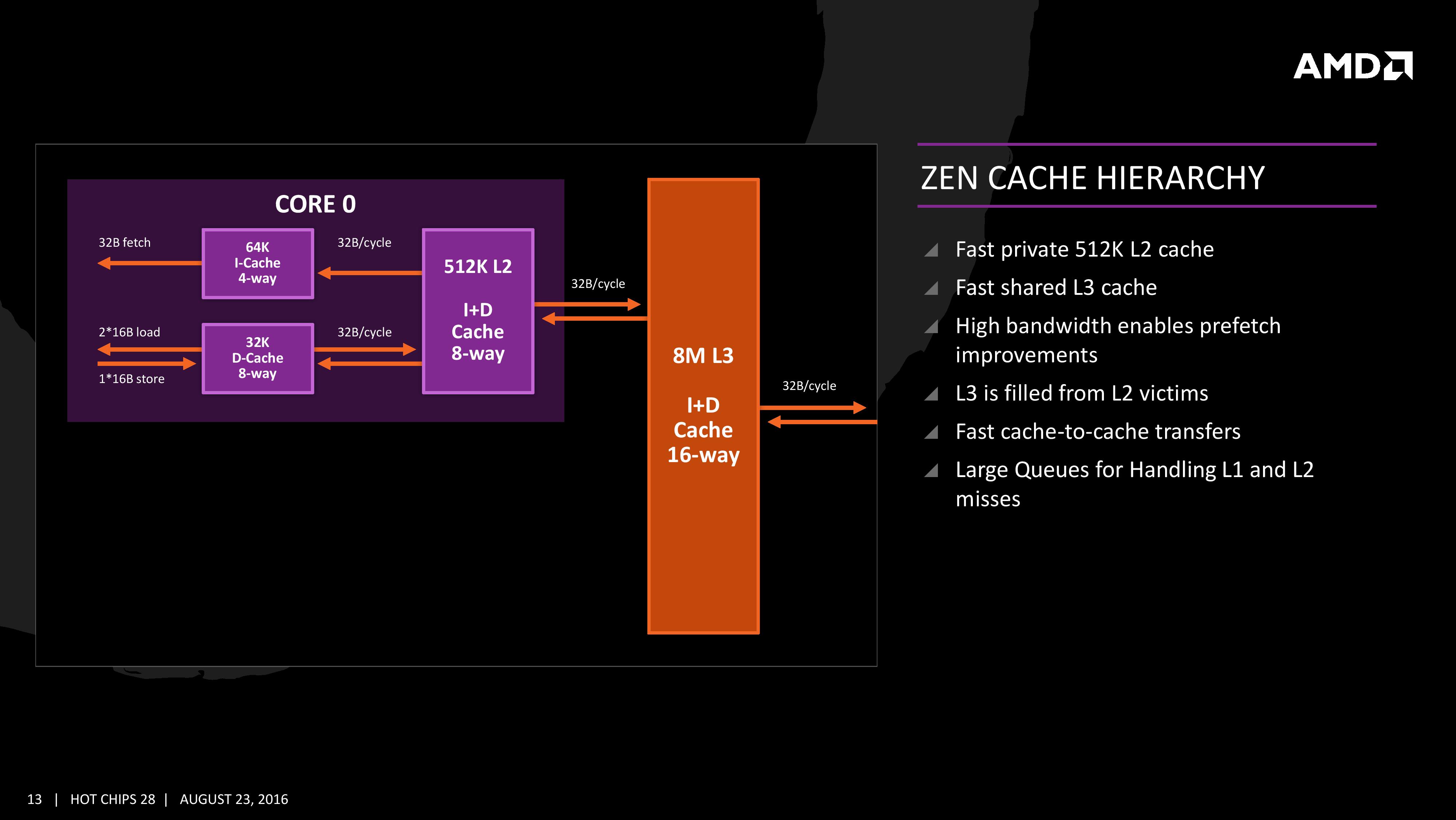
The cache representation in the new presentation at Hot Chips is almost identical to that in midweek, showing L1 and L2 in the core with 8MB of L3 split over several cores. AMD states that the L1 and L2 bandwidth is nearly double that of Excavator, with L3 now up to 5x for bandwidth, and that this bandwidth will help drive the improvements made on the prefetch side. AMD also states that there are large queues in play for L1/L2 cache misses.


106 Comments
View All Comments
eldakka - Wednesday, August 24, 2016 - link
The first page link, AMD Server CPUs and Motherboard Analysis, is wrong, it actually links to the ARM v8-A article.atlantico - Friday, August 26, 2016 - link
Yes, it's also wrong here: http://www.anandtech.com/show/10585/unpacking-amds...Sigh.
TristanSDX - Wednesday, August 24, 2016 - link
Zen do not support transactional memory, big disadvantage comparing to IntelSenti - Wednesday, August 24, 2016 - link
And how much does it matter? TSX is great thing no doubt there. But the adoption? What can you name of real software what uses and get significant benefit of it?I blame Intel stupid marketing for cutting TSX from too many versions and killing the adoption.
coder111 - Wednesday, August 24, 2016 - link
As far as I know, Azul JVMs do support transactional memory. So if you have a Java app, you can use it.Other than that, yes, I haven't seen TSX used much...
68k - Wednesday, August 24, 2016 - link
Isn't the version of glibc in recent Linux-distributions using the lock elision feature of TSX?https://lwn.net/Articles/534758/
https://01.org/blogs/tlcounts/2014/lock-elision-gl...
If so, then essentially every single Linux program does make use of TSX when present.
looncraz - Wednesday, August 24, 2016 - link
One of the most important features of TSX are checkpoints. Zen supports checkpoints in its execution pipeline. Otherwise, I've not seen anything that said Zen did or did not support TSX, not that the tech is widely used at this time.From there, you just need tagging and a few other features to add support. It's something that could be included in Zen+ if Zen does not have it.
silverblue - Wednesday, August 24, 2016 - link
It looks like Zen was developed to accelerate the vast majority of software, and rely on core count for everything else. It might explain the lack of focus on AVX.If cache stats were any indication of performance, it would appear that Zen was destined to compete with Broadwell, but not quite match the Lake CPUs; Zen+ would perhaps close the gap albeit a bit late. Bulldozer was hamstrung by half-speed writes and horrific L3 latency - would it be remiss to assume that they've at least fixed those two issues?
I'm not sure anybody can truly predict performance however, even with a Blender demonstration, and certainly not to work out prospective Cinebench or SuperPi performance. You could have a monster of an architecture, but if the software isn't optimised for it, it's not going to be representative of its true performance.
wumpus - Wednesday, August 24, 2016 - link
I'd still want the TSX instructions before even thinking about the server market. I guess they surrendered that before the overall architecture was finished. Although considering how badly it has worked for Intel (essentially turned off after errata was noted in the first generation), maybe it wasn't worth risk.Alexvrb - Sunday, August 28, 2016 - link
Yeah they need to take their time. A faulty implementation would do more harm than good at this point.