AMD Zen Microarchiture Part 2: Extracting Instruction-Level Parallelism
by Ian Cutress on August 23, 2016 8:45 PM EST- Posted in
- CPUs
- AMD
- x86
- Zen
- Microarchitecture
Execution, Load/Store, INT and FP Scheduling
The execution of micro-ops get filters into the Integer (INT) and Floating Point (FP) parts of the core, which each have different pipes and execution ports. First up is the Integer pipe which affords a 168-entry register file which forwards into four arithmetic logic units and two address generation units. This allows the core to schedule six micro-ops/cycle, and each execution port has its own 14-entry schedule queue.
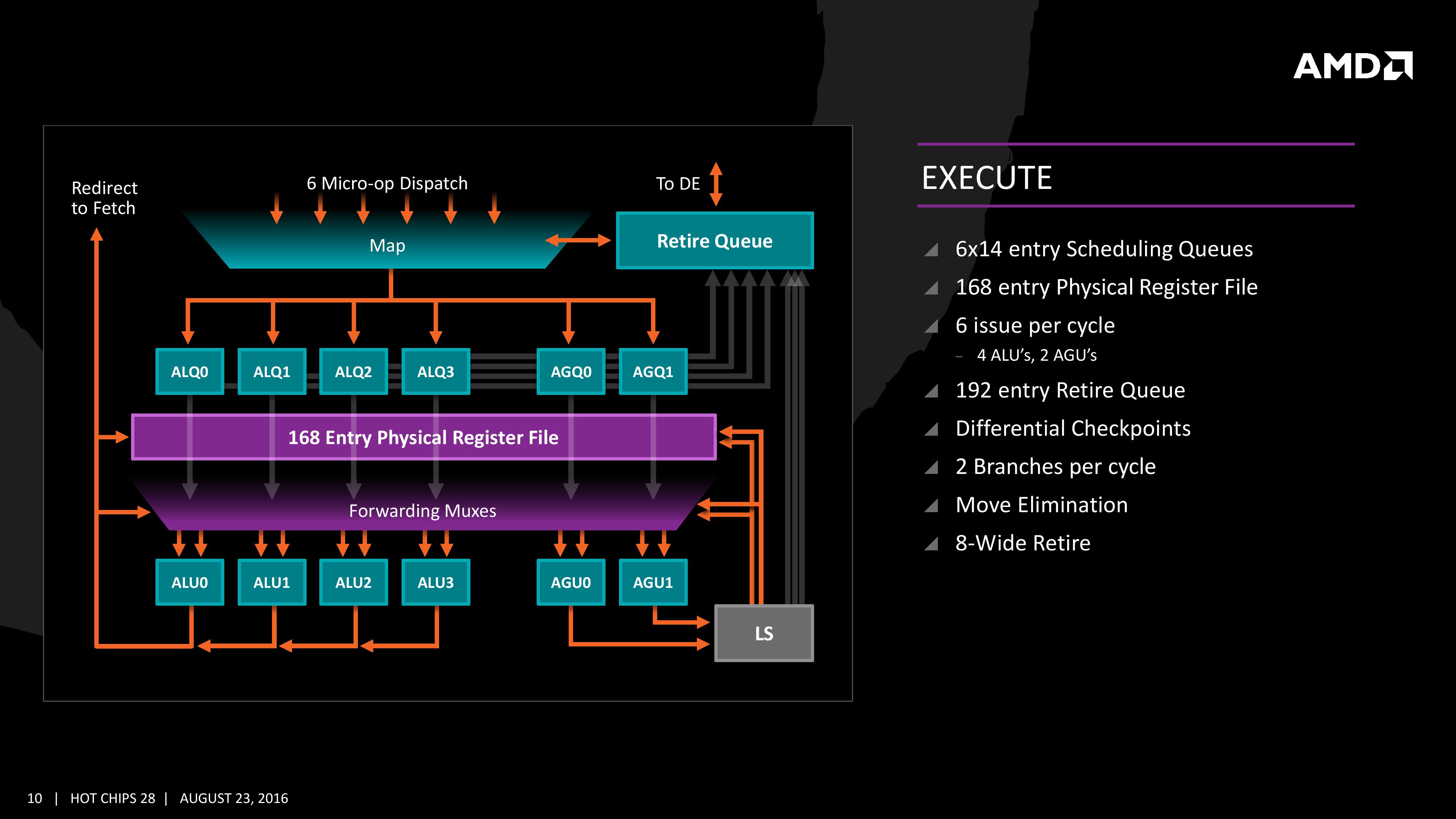
The INT unit can work on two branches per cycle, but it should be noted that not all the ALUs are equal. Only two ALUs are capable of branches, one of the ALUs can perform IMUL operations (signed multiply), and only one can do CRC operations. There are other limitations as well, but broadly we are told that the ALUs are symmetric except for a few focused operations. Exactly what operations will be disclosed closer to the launch date.
The INT pipe will keep track of branching instructions with differential checkpoints, to cut down on storing redundant data between branches (saves queue entries and power), but can also perform Move Elimination. This is where a simple mov command between two registers occurs – instead of inflicting a high energy loop around the core to physically move the single instruction, the core adjusts the pointers to the registers instead and essentially applies a new mapping table, which is a lower power operation.
Both INT and FP units have direct access to the retire queue, which is 192-entry and can retire 8 instructions per cycle. In some previous x86 CPU designs, the retire unit was a limiting factor for extracting peak performance, and so having it retire quicker than dispatch should keep the queue relatively empty and not near the limit.
The Load/Store Units are accessible from both AGUs simultaneously, and will support 72 out-of-order loads. Overall, as mentioned before, the core can perform two 16B loads (2x128-bit) and one 16B store per cycle, with the latter relying on a 44-entry Store queue. The TLB buffer for the L2 cache for already decoded addresses is two level here, with the L1 TLB supporting 64-entry at all page sizes and the L2 TLB going for 1.5K-entry with no 1G pages. The TLB and data pipes are split in this design, which relies on tags to determine if the data is in the cache or to start the data prefetch earlier in the pipeline.
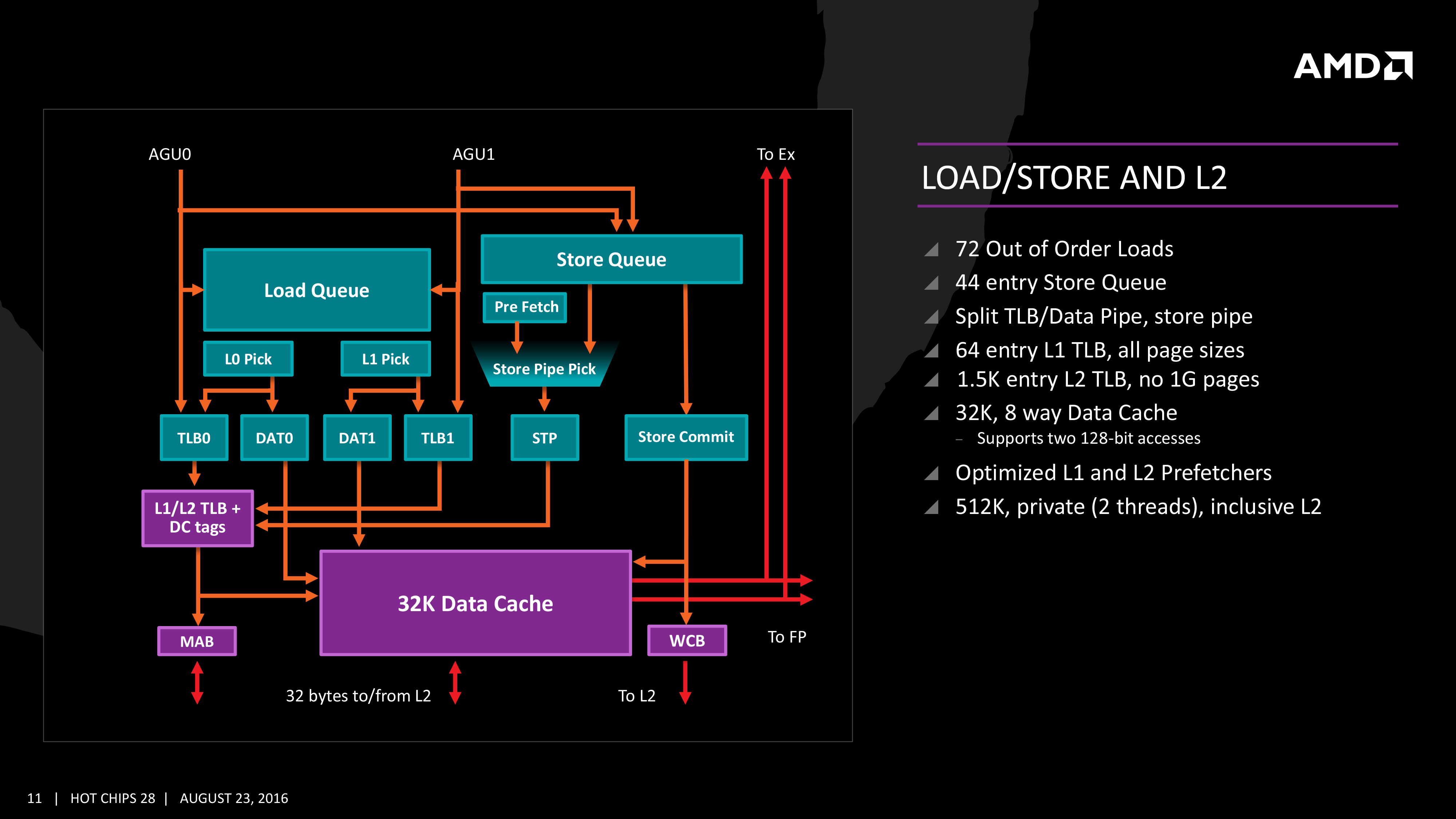
The data cache here also has direct access to the main L2 cache at 32 Bytes/cycle, with the 512 KB 8-way L2 cache being private to the core and inclusive. When data resides back in L1 it can be processed back to either the INT or the FP pipes as required.
Moving onto the floating point part of the core, and the first thing to notice is that there are two scheduling queues here. These are listed as ‘schedulable’ and ‘non-schedulable’ queues with lower power operation when certain micro-ops are in play, but also allows the backup queue to sort out parts of the dispatch in advance via the LDCVT. The register file is 160 entry, with direct FP to INT transfers as required, as well as supporting accelerated recovery on flushes (when data is written to a cache further back in the hierarchy to make room).
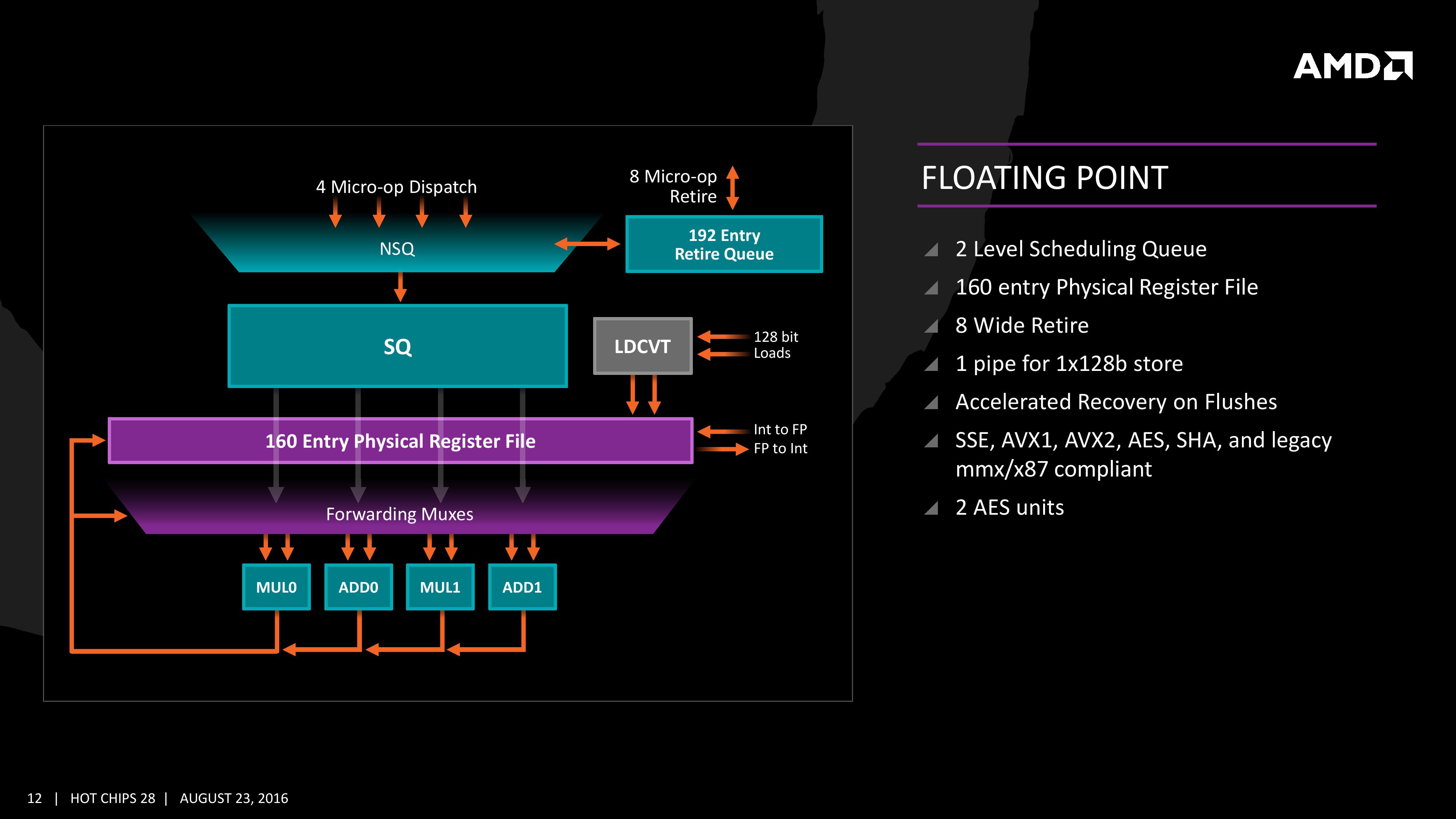
The FP Unit uses four pipes rather than three on Excavator, and we are told that the latency in Zen is reduced as well for operations (though more information on this will come at a later date). We have two MUL and two ADD in the FP unit, capable of joining to form two 128-bit FMACs, but not one 256-bit AVX. In order to do AVX, the unit will split the operations accordingly. On the counter side each core will have 2 AES units for cryptography as well as decode support for SSE, AVX1/2, SHA and legacy mmx/x87 compliant code.


106 Comments
View All Comments
atlantico - Friday, August 26, 2016 - link
Wow looncraz!! Really cool effort you made :)Spunjji - Saturday, August 27, 2016 - link
You numbers are different to everyone else's. Given that you don't cite any of your sources I believe everyone else.Krysto - Wednesday, August 24, 2016 - link
I would hope they try to double the cores of Intel for notebooks.Dual-core Zen without SMT will DESTROY Intel's Atom-based Celerons and Pentiums at the low-end. There will be absolutely ZERO reason to get a Celeron or Pentium notebooks once Zen appears on the market at that price range.
But at the Core i3 and Core i5 levels, I was hoping AMD would price a quad-core Zen with no SMT against dual-core Core i3 and Core i5, and a quad-core Zen with SMT against Intel's quad-core (no HT) Core i5, and finally 8-core with and without SMT variants against Intel's quad-core Core i7 chips (with HT).
If they can basically double the cores compared to what Intel has to offer at around the same price level, and maybe with only slightly worse single-thread performance and slightly worse power consumption, AMD's chips should be a NO-BRAINER. The value would be incredible, and it would push the market towards having powerful quad-core chips by default for most PCs. Intel is going to HATE that, because it would seriously cut into their profits. So AMD could use that strategy to both offer great value products and hurt Intel significantly.
looncraz - Wednesday, August 24, 2016 - link
AMD is not seeking the low end, they are trying to redefine AMD as the top-tier CPU company they once were. They are aiming for the top and the bulk of the market.Zen+'s 15% IPC improvement over Zen might just give them the performance crown, but I'm sure Intel has taken note and planned accordingly.
zaza - Wednesday, August 24, 2016 - link
but the AMD CCX module is a quad core module. i am not sure if it is easy for AMD to just remove two.looncraz - Wednesday, August 24, 2016 - link
Very easy, you just fuse off the defective core, that's the beauty of independent cores. The core complex just shares a common data bus and third level cache. Disabling a core in the complex will simply have it not ask for data on the common data bus. The L3 cache may or may not be cut down (probably will be).H2323 - Wednesday, August 24, 2016 - link
"While Zen is initially a high-performance x86 core at heart, it is designed to scale all the way from notebooks to supercomputers, or from where the Cat cores (such as Jaguar and Puma) were all the way up to the old Opterons and beyond, all with at least +40% IPC."https://www.youtube.com/watch?v=eUSJfGehKDQ
In the video its more than 40% across all of internal texting.
Vigilant007 - Saturday, August 27, 2016 - link
I don't know if AMD will ever have a major win as far as the PC industry again. Realistically they'll end up focusing on building custom x86 for consoles, and server chips. I can also see them exploiting their ability to do x86 to design custom chips for Apple.AMD could end up being a fantastic acquisition target as well.
Tuna-Fish - Tuesday, August 23, 2016 - link
From page 3:> and L2 with 512 entries and support for 4K and 256K pages only.
Surely you meant 4k and 2MB pages only?
deltaFx2 - Tuesday, August 23, 2016 - link
Ian, an error here: "It also states that the L3 is mostly inclusive of the L2 cache, which stems from the L3 cache as a victim cache for L2 data." A victim L3 is by definition an exclusive cache (as you note elsewhere). Also I don't understand why you have the impression that a victim cache is less efficient than an inclusive cache. As you note, an inclusive cache has to keep duplicate copies of data in L2 and L3 whereas an exclusive cache stores exactly 1 copy (either L2 or L3 but never both). In an exclusive cache hierarchy, a cache block is inserted into the L2, and when evicted, is put into the L3. In an inclusive cache hierarchy, a cache block is inserted both into the L2 and L3. Doesn't the exclusive hierarchy make better use of space? Incidentally, AMD has done exclusive caches since K8 at least. This isn't new.