AMD Zen Microarchiture Part 2: Extracting Instruction-Level Parallelism
by Ian Cutress on August 23, 2016 8:45 PM EST- Posted in
- CPUs
- AMD
- x86
- Zen
- Microarchitecture
Some Final Thoughts and Comparisons
With the Hot Chips presentation we’ve been given more information on the Zen core microarchitecture than we expected to have at this point in the Zen design/launch cycle. AMD has already stated that general availability for Zen will be in Q1, and Zen might not be the final product launch name/brand when it comes to market. However, there are still plenty of gaps in our knowledge for the hardware, and AMD has promised to reveal this information as we get closer to launch.
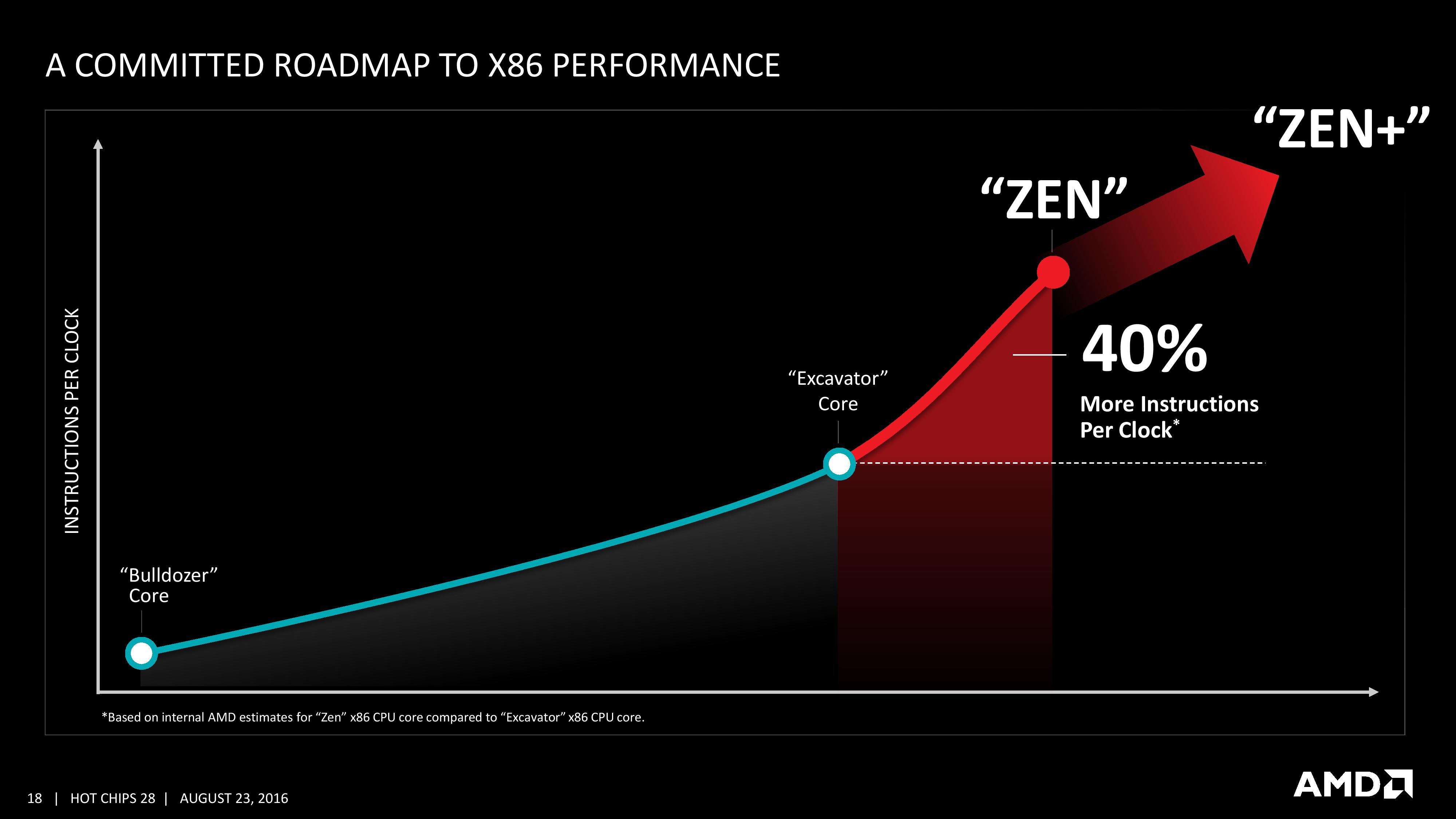
We discussed in our earlier piece on the Zen performance metrics given mid-week that it can be hard to interpret any anecdotal benchmark data at this point when there is so much we don’t know (or can’t confirm). With the data in this talk at Hot Chips, we can fill out a lot of information for a direct comparison chart to AMD’s last product and Intel’s current offerings.
| CPU uArch Comparison | ||||
| AMD | Intel | |||
| Zen 8C/16T 2017 |
Bulldozer 4M / 8T 2010 |
Skylake 4C / 8T 2015 |
Broadwell 8C / 16T 2014 |
|
| L1-I Size | 64KB/core | 64KB/module | 32KB/core | 32KB/core |
| L1-I Assoc | 4-way | 2-way | 8-way | 8-way |
| L1-D Size | 32KB/core | 16KB/thread | 32KB/core | 32KB/core |
| L1-D Assoc | 8-way | 4-way | 8-way | 8-way |
| L2 Size | 512KB/core | 1MB/thread | 256KB/core | 256KB/core |
| L2 Assoc | 8-way | 16-way | 4-way | 8-way |
| L3 Size | 2MB/core | 1MB/thread | >2MB/cire | 1.5-3MB/core |
| L3 Assoc | 16-way | 64-way | 16-way | 16/20-way |
| L3 Type | Victim | Victim | Write-back | Write-back |
| L0 ITLB Entry | 8 | - | - | - |
| L0 ITLB Assoc | ? | - | - | - |
| L1 ITLB Entry | 64 | 72 | 128 | 128 |
| L1 ITLB Assoc | ? | Full | 8-way | 4-way |
| L2 ITLB Entry | 512 | 512 | 1536 | 1536 |
| L2 ITLB Assoc | ? | 4-way | 12-way | 4-way |
| L1 DTLB Entry | 64 | 32 | 64 | 64 |
| L1 DTLB Assoc | ? | Full | 4-way | 4-way |
| L2 DTLB Entry | 1536 | 1024 | - | - |
| L2 DTLB Assoc | ? | 8-way | - | - |
| Decode | 4 uops/cycle | 4 Mops/cycle | 5 uops/cycle | 4 uops/cycle |
| uOp Cache Size | ? | - | 1536 | 1536 |
| uOp Cache Assoc | ? | - | 8-way | 8-way |
| uOp Queue Size | ? | - | 128 | 64 |
| Dispatch / cycle | 6 uops/cycle | 4 Mops/cycle | 6 uops/cycle | 4 uops/cycle |
| INT Registers | 168 | 160 | 180 | 168 |
| FP Registers | 160 | 96 | 168 | 168 |
| Retire Queue | 192 | 128 | 224 | 192 |
| Retire Rate | 8/cycle | 4/cycle | 8/cycle | 4/cycle |
| Load Queue | 72 | 40 | 72 | 72 |
| Store Queue | 44 | 24 | 56 | 42 |
| ALU | 4 | 2 | 4 | 4 |
| AGU | 2 | 2 | 2+2 | 2+2 |
| FMAC | 2x128-bit | 2x128-bit 2x MMX 128-bit |
2x256-bit | 2x256-bit |
Bulldozer uses AMD-coined macro-ops, or Mops, which are internal fixed length instructions and can account for 3 smaller ops. These AMD Mops are different to Intel's 'macro-ops', which are variable length and different to Intel's 'micro-ops', which are simpler and fixed-length.
Excavator has a number of improvements over Bulldozer, such as a larger L1-D cache and a 768-entry L1 BTB size, however we were never given a full run-down of the core in a similar fashion and no high-end desktop version of Excavator will be made.
This isn’t an exhaustive list of all features (thanks to CPU World, Real World Tech and WikiChip for filling in some blanks) by any means, and doesn’t paint the whole story. For example, on the power side of the equation, AMD is stating that it has the ability to clock gate parts of the core and CCX that are not required to save power, and the L3 runs on its own clock domain shared across the cores. Or the latency to run certain operations, which is critical for workflow if a MUL operation takes 3, 4 or 5 cycles to complete. We have been told that the FPU load is two cycles quicker, which is something. The latency in the caches is also going to feature heavily in performance, and all we are told at this point is that L2 and L3 are lower latency than previous designs.
A number of these features we’ve already seen on Intel x86 CPUs, such as move elimination to reduce power, or the micro-op cache. The micro-op cache is a piece of the puzzle we want to know more about, especially the rate at which we get cache hits for a given workload. Also, the use of new instructions will adjust a number of workloads that rely on them. Some users will lament the lack of true single-instruction AVX-2 support, however I suspect AMD would argue that the die area cost might be excessive at this time. That’s not to say AMD won’t support it in the future – we were told quite clearly that there were a number of features originally listed internally for Zen which didn’t make it, either due to time constraints or a lack of transistors.
We are told that AMD has a clear internal roadmap for CPU microarchitecture design over the next few generations. As long as we don’t stay for so long on 14nm similar to what we did at 28/32nm, with IO updates over the coming years, a competitive clock-for-clock product (even to Broadwell) with good efficiency will be a welcome return.


106 Comments
View All Comments
Tucker Smith - Thursday, August 25, 2016 - link
I hear much regarding the potential of Zen in comparison to Intel's HEDT procs, but, given AMD's touting of Zen's scalability, can we glean insight into how it will compete in the $100 range against the i3? People have been clamoring for an unlocked 2c/4t. The excitement over the potential to OC via BCLK on the Skylake was huge, the disappointment when Intel reneged on it even larger.The Kaveri-based Athlon x4 860k and the Carrizo Athlon, the 845, were fine chips under $100, but the limited cache and platform options kinda turned me off. A small Zen proc with one of the new, nicer cooling solutions they're offering on a modern mobo sounds incredibly compelling.
I hear much regarding 8c/16t chips, a lot about potential APUs, but what about that broad middle ground?
iranterres - Thursday, August 25, 2016 - link
Tucker Smith, you made an excellent point. But I think they will launch zen based stuff to compete all across the boardfanofanand - Thursday, August 25, 2016 - link
Zen is the architecture, not necessarily the name of the processor family. They have mentioned the scalability up and down the chain, indicating that they will indeed populate their entire processor line with the Zen architecture. It's impossible to know how well they will scale until they are in independent tester's hands, but I would imagine they have learned quite a bit from their Jaguar cores and should be able to put together a compelling offering in the sub $100 range.Outlander_04 - Thursday, August 25, 2016 - link
AMD sell APU's with disabled graphics cores already, as well as a range of 2 module APU's with minimal graphics .That is the ground you are talking about surely?
alpha754293 - Tuesday, August 30, 2016 - link
It WOULD be interesting to see how they perform in floating point intensive benchmarks compare to their Intel counterparts given the architectural differences between the two company's approaches.tipoo - Wednesday, August 31, 2016 - link
Last table - >2MB/cire