AMD Zen Microarchiture Part 2: Extracting Instruction-Level Parallelism
by Ian Cutress on August 23, 2016 8:45 PM EST- Posted in
- CPUs
- AMD
- x86
- Zen
- Microarchitecture
The Core Complex, Caches, and Fabric
Many core designs often start with an initial low-core-count building block that is repeated across a coherent fabric to generate a large number of cores and the large die. In this case, AMD is using a CPU Complex (CCX) as that building block which consists of four cores and the associated caches.
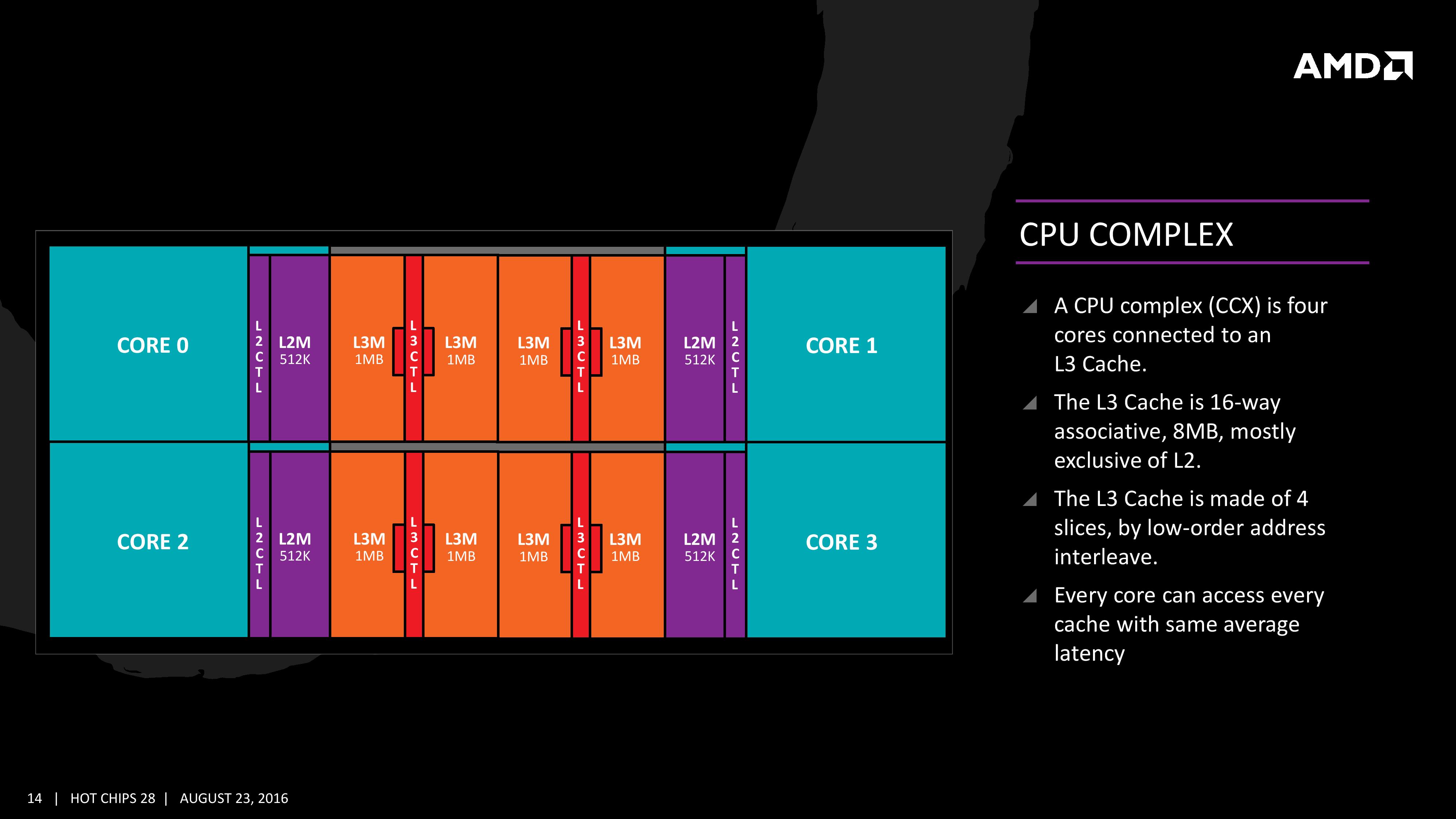
Each core will have direct access to its private L2 cache, and the 8 MB of L3 cache is, despite being split into blocks per core, accessible by every core on the CCX with ‘an average latency’ also L3 hits nearer to the core will have a lower latency due to the low-order address interleave method of address generation.
The L3 cache is actually a victim cache, taking data from L1 and L2 evictions rather than collecting data from prefetch/demand instructions. Victim caches tend to be less effective than inclusive caches, however Zen counters this by having a sufficiency large L2 to compensate. The use of a victim cache means that it does not have to hold L2 data inside, effectively increasing its potential capacity with less data redundancy.
It is worth noting that a single CCX has 8 MB of cache, and as a result the 8-core Zen being displayed by AMD at the current events involves two CPU Complexes. This affords a total of 16 MB of L3 cache, albeit in two distinct parts. This means that the true LLC for the entire chip is actually DRAM, although AMD states that the two CCXes can communicate with each other through the custom fabric which connects both the complexes, the memory controller, the IO, the PCIe lanes etc.
One interesting story is going to be how AMD’s coherent fabric works. For those that follow mobile phone SoCs, we know fabrics and interconnects such as CCI-400 or the CCN family are optimized to take advantage of core clusters along with the rest of the chip. A number of people have speculated that the fabric used in AMD’s new design is based on HyperTransport, however AMD has confirmed that they are not using HyperTransport here for Zen. More information on the fabric may come out as we nearer the launch, although this remains one of the more mysterious elements to the design at this stage.
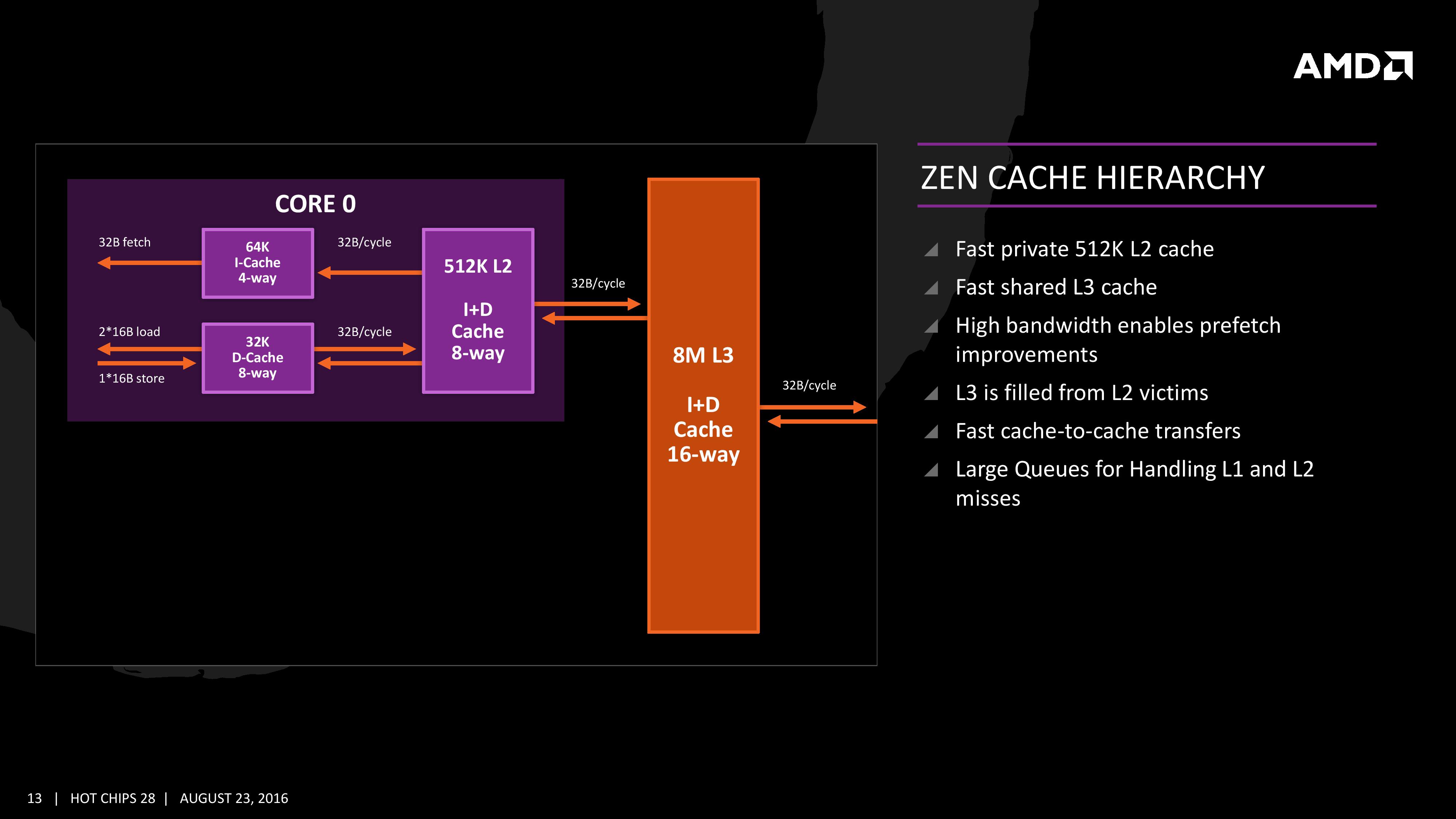
The cache representation in the new presentation at Hot Chips is almost identical to that in midweek, showing L1 and L2 in the core with 8MB of L3 split over several cores. AMD states that the L1 and L2 bandwidth is nearly double that of Excavator, with L3 now up to 5x for bandwidth, and that this bandwidth will help drive the improvements made on the prefetch side. AMD also states that there are large queues in play for L1/L2 cache misses.


106 Comments
View All Comments
Tucker Smith - Thursday, August 25, 2016 - link
I hear much regarding the potential of Zen in comparison to Intel's HEDT procs, but, given AMD's touting of Zen's scalability, can we glean insight into how it will compete in the $100 range against the i3? People have been clamoring for an unlocked 2c/4t. The excitement over the potential to OC via BCLK on the Skylake was huge, the disappointment when Intel reneged on it even larger.The Kaveri-based Athlon x4 860k and the Carrizo Athlon, the 845, were fine chips under $100, but the limited cache and platform options kinda turned me off. A small Zen proc with one of the new, nicer cooling solutions they're offering on a modern mobo sounds incredibly compelling.
I hear much regarding 8c/16t chips, a lot about potential APUs, but what about that broad middle ground?
iranterres - Thursday, August 25, 2016 - link
Tucker Smith, you made an excellent point. But I think they will launch zen based stuff to compete all across the boardfanofanand - Thursday, August 25, 2016 - link
Zen is the architecture, not necessarily the name of the processor family. They have mentioned the scalability up and down the chain, indicating that they will indeed populate their entire processor line with the Zen architecture. It's impossible to know how well they will scale until they are in independent tester's hands, but I would imagine they have learned quite a bit from their Jaguar cores and should be able to put together a compelling offering in the sub $100 range.Outlander_04 - Thursday, August 25, 2016 - link
AMD sell APU's with disabled graphics cores already, as well as a range of 2 module APU's with minimal graphics .That is the ground you are talking about surely?
alpha754293 - Tuesday, August 30, 2016 - link
It WOULD be interesting to see how they perform in floating point intensive benchmarks compare to their Intel counterparts given the architectural differences between the two company's approaches.tipoo - Wednesday, August 31, 2016 - link
Last table - >2MB/cire