AMD Zen Microarchiture Part 2: Extracting Instruction-Level Parallelism
by Ian Cutress on August 23, 2016 8:45 PM EST- Posted in
- CPUs
- AMD
- x86
- Zen
- Microarchitecture
The High-Level Zen Overview
AMD is keen to stress that the Zen project had three main goals: core, cache and power. The power aspect of the design is one that was very aggressive – not in the sense of aiming for a mobile-first design, but efficiency at the higher performance levels was key in order to be competitive again. It is worth noting that AMD did not mention ‘die size’ in any of the three main goals, which is usually a requirement as well. Arguably you can make a massive core design to run at high performance and low latency, but it comes at the expense of die size which makes the cost of such a design from a product standpoint less economical (if AMD had to rely on 500mm2 die designs in consumer at 14nm, they would be priced way too high). Nevertheless, power was the main concern rather than pure performance or function, which have been typical AMD targets in the past. The shifting of the goal posts was part of the process to creating Zen.
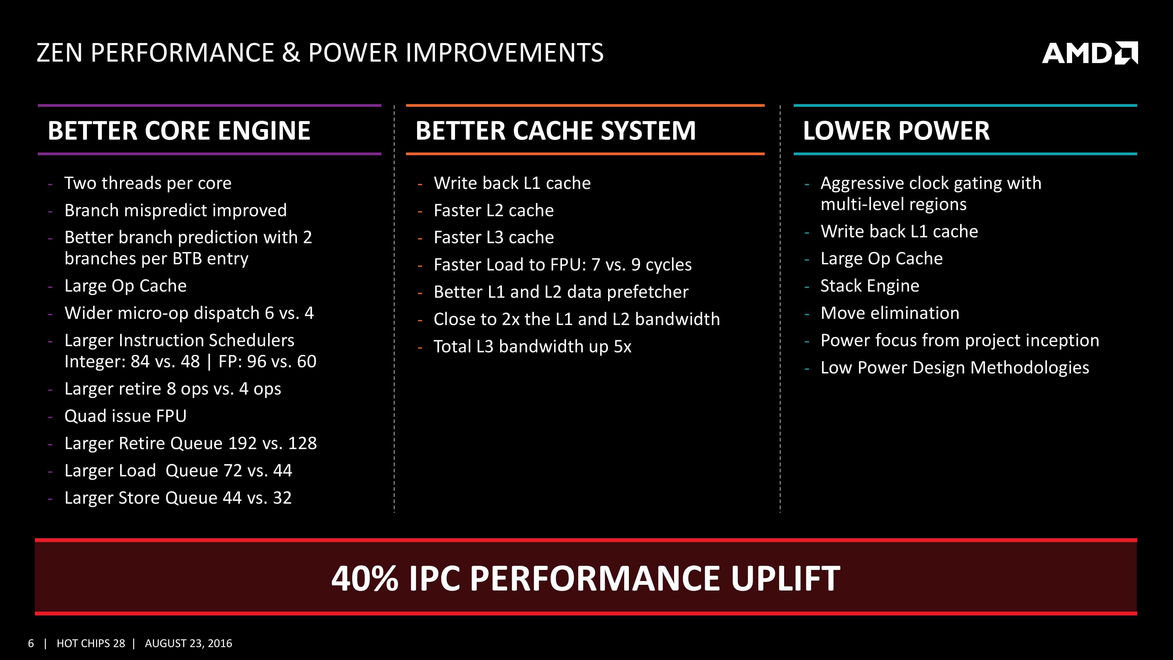
This slide contains a number of features we will hit on later in this piece but covers a number of main topics which come under those main three goals of core, cache and power.
For the core, having bigger and wider everything was to be expected, however maintaining a low latency can be difficult. Features such as the micro-op cache help most instruction streams improve in performance and bypass parts of potentially long-cycle repetitive operations, but also the larger dispatch, larger retire, larger schedulers and better branch prediction means that higher throughput can be maintained longer and in the fastest order possible. Add in dual threads and the applicability of keeping the functional units occupied with full queues also improves multi-threaded performance.
For the caches, having a faster prefetch and better algorithms ensures the data is ready when each of the caches when a thread needs it. Aiming for faster caches was AMD’s target, and while they are not disclosing latencies or bandwidth at this time, we are being told that L1/L2 bandwidth is doubled with L3 up to 5x.
For the power, AMD has taken what it learned with Carrizo and moved it forward. This involves more aggressive monitoring of critical paths around the core, and better control of the frequency and power in various regions of the silicon. Zen will have more clock regions (it seems various parts of the back-end and front-end can be gated as needed) with features that help improve power efficiency, such as the micro-op cache, the Stack Engine (dedicated low power address manipulation unit) and Move elimination (low-power method for register adjustment - pointers to registers are adjusted rather than going through the high-power scheduler).
The Big Core Diagram
We saw this diagram last week, but now we get updates on some of the bigger features AMD wants to promote:
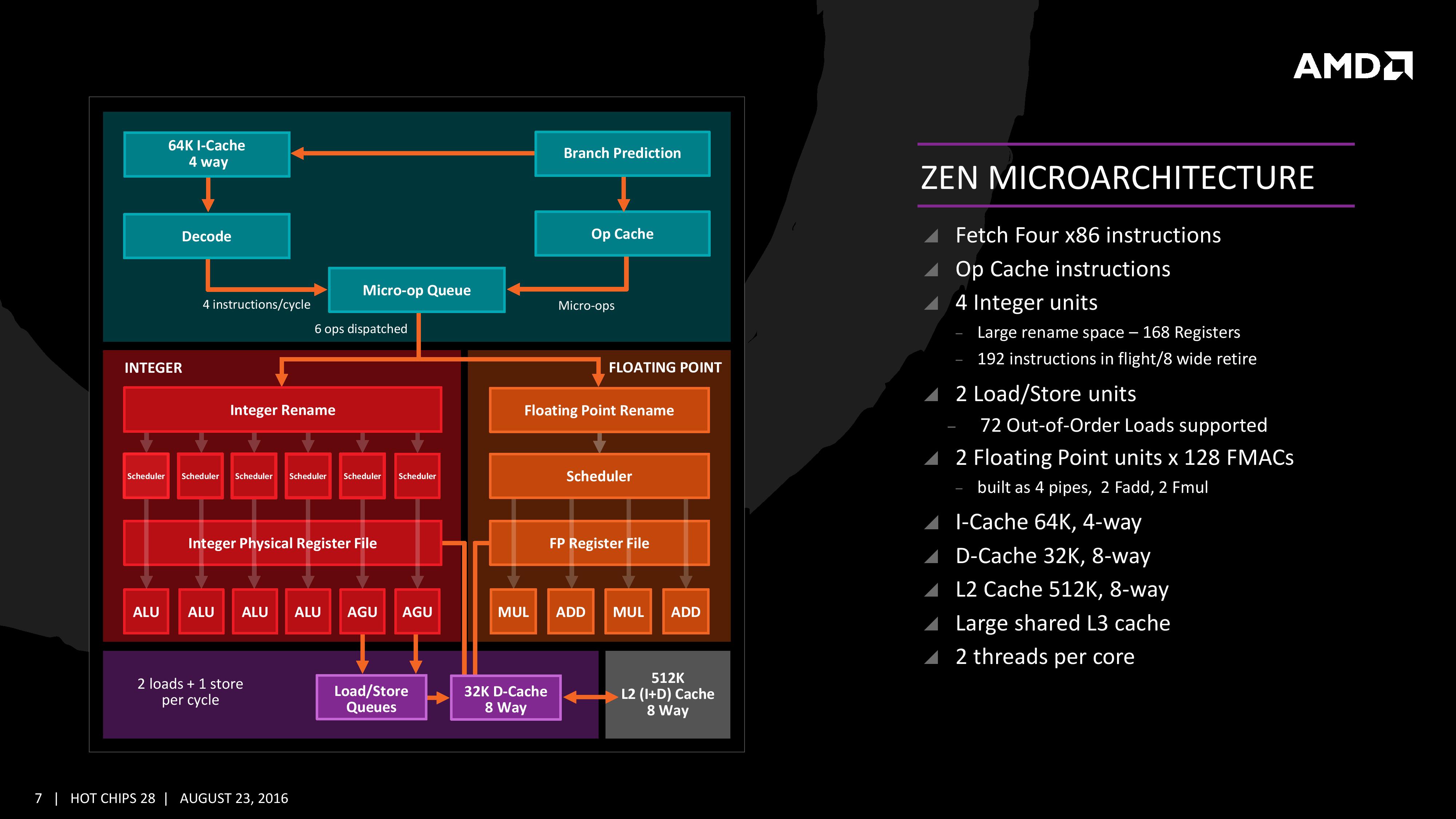
The improved branch predictor allows for 2 branches per Branch Target Buffer (BTB), but in the event of tagged instructions will filter through the micro-op cache. On the other side, the decoder can dispatch 4 instructions per cycle however some of those instructions can be fused into the micro-op queue. Fused instructions still come out of the queue as two micro-ops, but take up less buffer space as a result.
As mentioned earlier, the INT and FP pipes and schedulers are separated, but the INT rename space is 168 registers wide, which feeds into 6x14 scheduling queues. The FP employs as 160 entry register file, and both the FP and INT sections feed into a 192-entry retire queue. The retire queue can operate at 8 instructions per cycle, moving up from 4/cycle in previous AMD microarchitectures.
The load/store units are improved, supporting a 72 out-of-order loads, similar to Skylake. We’ll discuss this a bit later. On the FP side there are four pipes (compared to three in previous designs) which support combined 128-bit FMAC instructions. These cannot be combined for one 256-bit AVX2, but can be scheduled for AVX2 over two instructions.


106 Comments
View All Comments
Tucker Smith - Thursday, August 25, 2016 - link
I hear much regarding the potential of Zen in comparison to Intel's HEDT procs, but, given AMD's touting of Zen's scalability, can we glean insight into how it will compete in the $100 range against the i3? People have been clamoring for an unlocked 2c/4t. The excitement over the potential to OC via BCLK on the Skylake was huge, the disappointment when Intel reneged on it even larger.The Kaveri-based Athlon x4 860k and the Carrizo Athlon, the 845, were fine chips under $100, but the limited cache and platform options kinda turned me off. A small Zen proc with one of the new, nicer cooling solutions they're offering on a modern mobo sounds incredibly compelling.
I hear much regarding 8c/16t chips, a lot about potential APUs, but what about that broad middle ground?
iranterres - Thursday, August 25, 2016 - link
Tucker Smith, you made an excellent point. But I think they will launch zen based stuff to compete all across the boardfanofanand - Thursday, August 25, 2016 - link
Zen is the architecture, not necessarily the name of the processor family. They have mentioned the scalability up and down the chain, indicating that they will indeed populate their entire processor line with the Zen architecture. It's impossible to know how well they will scale until they are in independent tester's hands, but I would imagine they have learned quite a bit from their Jaguar cores and should be able to put together a compelling offering in the sub $100 range.Outlander_04 - Thursday, August 25, 2016 - link
AMD sell APU's with disabled graphics cores already, as well as a range of 2 module APU's with minimal graphics .That is the ground you are talking about surely?
alpha754293 - Tuesday, August 30, 2016 - link
It WOULD be interesting to see how they perform in floating point intensive benchmarks compare to their Intel counterparts given the architectural differences between the two company's approaches.tipoo - Wednesday, August 31, 2016 - link
Last table - >2MB/cire