Ten Year Anniversary of Core 2 Duo and Conroe: Moore’s Law is Dead, Long Live Moore’s Law
by Ian Cutress on July 27, 2016 10:30 AM EST- Posted in
- CPUs
- Intel
- Core 2 Duo
- Conroe
- ITRS
- Nostalgia
- Time To Upgrade
Looking To The Future: 450mm Wafers in 2021, and Down to ‘2nm’
Most users following the industry will know that the name of the lithographic node, such as ‘14nm’, ‘16nm’ or ‘28nm’ is often an imperfect characterization of what is actually happening on the silicon. For example, Intel’s 14nm node is widely touted as the best in the industry, and the equivalent 14nm/16nm nodes are said to not be even close, due to Intel’s focus on several generations of FinFET compared to the other main semiconductor manufacturers. This also means that while ‘14nm’ or ‘16nm’ is mentioned, many other parts of the silicon could be manufactured on other nodes, depending on the utility.
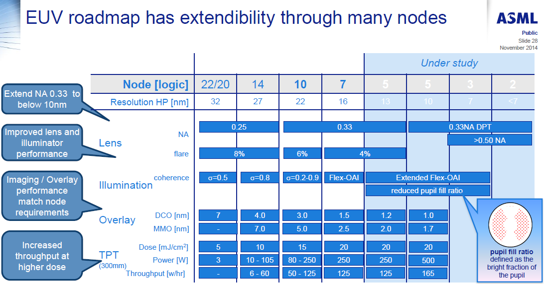
We’ve spoken in the past about equipment roadmaps to deal with the problem of shrinking lithography node sizes. This includes new lasers, droplet generation, collectors, masks, defect detection, lenses, and the technology to drive high throughput. For example, here are ASML’s EUV requirements for the next few manufacturing nodes, including requirements for 250W light sources at a 5nm node:
With the ITRS report, it makes a couple of metrics regarding node sizes and wafers. On the later, we get the prediction that 450mm wafers should be in play at around 2021 for DRAM:
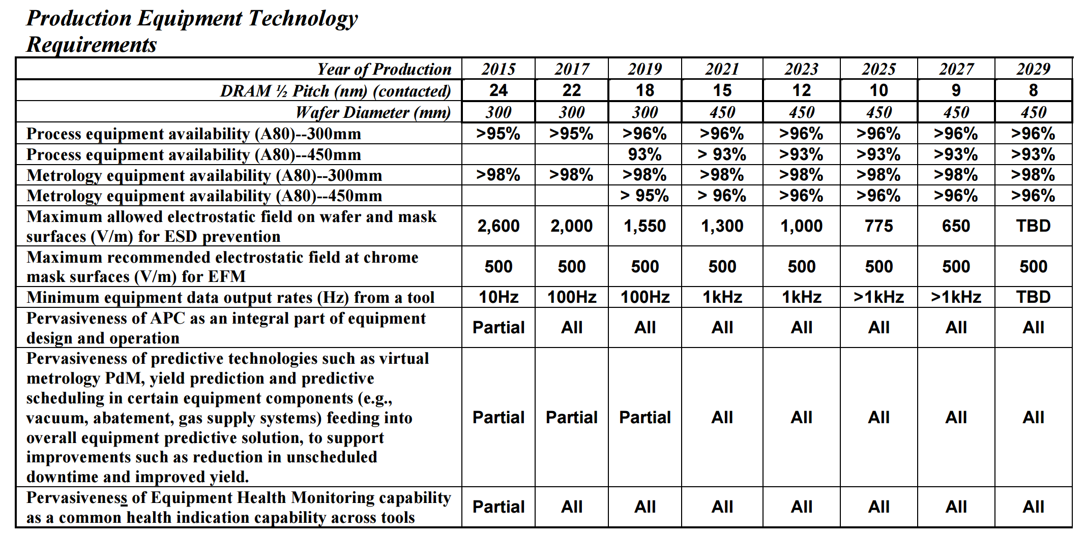
This matches at DRAM half-pitch of 15nm, or a DRAM cell size of 780nm2, compared to 3480nm2 today. The movement to 450mm wafers has been expected for some time, with early predictions going for the 2008-2011 timeframe, however development seems to have stalled for a variety of reasons.
When it comes to transistors, given the node naming scheme caveats listed above, the ITRS report predicts that FinFET will make way at around the 2021 timeframe in favor of 3D stacking such as ‘vertical gate all-around’ (VGAA). As the node shrinks, as well as the transistor size, the power supply voltage will drop from 800mV today down to 400/450mV by 2027.
![]()
Moving into a world of IoT will require even lower power transistors, of which moving to a ‘smaller node’ and vertical chip integration will be a large part.
The ITRS report goes into a lot of detail regarding different stacking technologies, such as the 2.5D integration we see on products like AMD’s Fiji GPU involving a silicon interposer, as well as 3D and the different ways to implement both microchannel cooling in such chips as well as 3D TSV applications.


158 Comments
View All Comments
pixelstuff - Wednesday, July 27, 2016 - link
I think Core2 essentially accelerated the market saturation we are seeing and causing the PC market to decline a bit. My Core2 E8400 still runs Window 10 relatively fine, although I have built two more since because I like being near the cutting edge. However I know quite a few people still using Core2 CPUs for their basic computing needs.There just haven't been any new apps that are more resource intensive than a word processor or web browser which the entire world needs. So the PC replacement market has stagnated a bit.
stardude82 - Wednesday, July 27, 2016 - link
Most Core processors are faster than the ho-hum Cherry Trail offerings you find low end PCs. So buying a new cute shiny black little box to replace your beige big box doesn't guarantee much.boeush - Wednesday, July 27, 2016 - link
It reads a little weird/myopic that only certain technologies are being considered while forecasting all the way out to 2030. For instance, lots of NAND/DRAM discussion but no mention of upcoming or already early-adoption tech like 3D XPoint or memristors, etc. No mention of optoelectronics (like photonic signalling on- and off-chip), no mention of III-V and other 'exotic' materials for chip manufacturing and improved frequency/power scaling (with focus instead devoted to feature sizes/stacking/platter size/defects.) And so on.I mean, if you're forecasting 5 years ahead, I'd understand. But talking about 15 years into the future but only extrapolating from what's on the market right now -- as opposed to what's in the labs and on drawing boards -- seems to be a little too pessimistic and/or myopic.
Ian Cutress - Wednesday, July 27, 2016 - link
The full report mentions III-V and SiGe in the remit of future technologies. Anton and I are starting to discuss what parts we can pull out for individual news stories, to stay tuned.Sam Snead - Wednesday, July 27, 2016 - link
Heck I still have my Nexgen P110 cpu computer set up and run it once in awhile. From 1996. Remember the VESA local bus video card? Nexgen was later bought by AMD.stardude82 - Wednesday, July 27, 2016 - link
Ah, I remember Socket 7...CoreLogicCom - Wednesday, July 27, 2016 - link
I've still got a Dell E1705 laptop that I bought in 2006 which came with a Core Duo, which I upgraded to Core 2 Duo about 4 years into it, and maxed the RAM to 4GB (from the 2GB max it came with). It was decent, but really came alive when I put an SSD into it. I still use this laptop for basic stuff, and even some gaming (WoW and SWToR) with the Geforce Go GPU. It's definitely long in the tooth now, now running Windows 7 (it came with WinXP, but 10 is unsupported on the GPU even though there's a work around). I'm thinking mobile Kaby Lake and mobile Pascal will be the next laptop I keep for another 10 years.Nacho - Wednesday, July 27, 2016 - link
Can you beat me?Last month I finally upgraded my primary rig from a C2D E4300 @2.7Ghz! Memory started failing last year & I couldn't find cheap DDR2, so I was down to 2GB.
Went for a i5 6500 and 16GB DDR4. The difference is incredible!
Filiprino - Wednesday, July 27, 2016 - link
So much time since reading Anand's article on Conroe.3ogdy - Wednesday, July 27, 2016 - link
Great article, Ian! I've found it a very good read and it's always nice to take a look back and analyze what we've been through so far.I also wanna point out just a few mini-errors I've found in the article:
The Core 2 processors all came from a 143mm2 die, compared TO the 162mm2 of Pentium D. /
by comparison to the large die sizes we see IN 2016 for things like the P100 /
whereas the popular Core 2 Duo E6400 at $224 WAS at the same price as the Core i5-6600.
As we NOW know, on-die IMCs are the big thing.
Geometrical Scaling when this could NO longer operate
By 2020-25 device features will be REDUCED (?)
On the later -> LATTER?
Keep up the amazing work!