SiS 730S Socket-A Chipset: Is the Duron allowed to succeed now?
by Anand Lal Shimpi on December 13, 2000 4:06 AM EST- Posted in
- CPUs
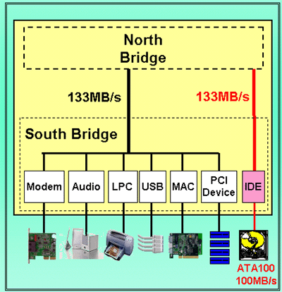
Conventional Chipset Design
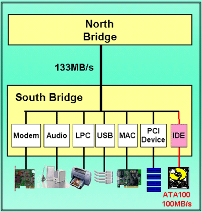
The final feature of importance surrounding the 730S is its ATA/100 controller. In conventional chipset designs, the IDE controller must share the 133MB/s bandwidth that the PCI bus offers with the rest of the PCI devices as well as your USB ports, etc… Intel’s Hub Architecture attempts to solve this problem by offering a wider 266MB/s bus connecting the I/O Controller to the Memory Controller (essentially the Northbridge). The 730S addresses this issue by providing the IDE channels with a dedicated 133MB/s pathway to the Northbridge. This should help alleviate any bottlenecks that may arise as ATA/100 drives come closer and closer to peaking at that 100MB/s limit of the specification.
SiS 730S Chipset Design
With all of the features that the 730S incorporates into a single physical chip, it is amazing that SiS can keep the price down to $39 in 10K quantities. This is almost identical to the cost of AMD’s 760 chipset, but this covers the cost of integrated video as well as all the normal functions of the chipset. This is approximately $6 more expensive than Intel’s 810E chipset, which can be expected since the 730S is a physically larger chip than both the GMCH and the ICH of the i810. This translates into more expensive system costs when you look at the big picture where hundreds upon thousands of these systems will be shipping. Whether this will, in the end, affect how competitive the Duron will be in comparison to the Celeron in the retail market has yet to be seen.


0 Comments
View All Comments