AMD 760MP & Athlon MP - Dual Processor Heaven
by Anand Lal Shimpi on June 5, 2001 12:00 PM EST- Posted in
- CPUs
Far from just 760
Just one year ago AMD promised that we'd see their first multiprocessor solution in Q3/Q4 of 2000. The AMD 770, as it was called, was to be paired up with the Mustang processor outfitted with a very large L2 cache. It may have been more appropriate to keep the name of the chipset as 770 since it is significantly different from the desktop 760 chipset, but AMD did decide to call it the 760MP.
The main reason that the 760MP would have been better off being called the
770 is its sheer size advantage over the desktop 760 chipset. The 760 chipset
is made up of two major parts, the AMD 761 North Bridge and the AMD 766 South
Bridge and the two are connected by the 32-bit/33MHz PCI bus. The 761 North
Bridge is manufactured in a BGA (Ball Grid Array) packaging with a total of
569-balls (essentially interface pins) that connect the chip to the various
buses and parts of the motherboard. The AMD 760MP on the other hand uses a
different
We mentioned earlier that the 760MP chipset features a Point-to-Point FSB protocol,
meaning that each processor in a 760MP system gets its own connection to the
North Bridge. Unfortunately, this means that there are significantly more traces
going between the
The benefits of the Point-to-Point FSB are numerous. We’ve already explained the benefits when it comes to inner-CPU communication (although the tangible performance benefits resulting from this may be limited), but there is obviously a much larger benefit: an increase in overall FSB bandwidth.
Each Athlon MP gets 2.1GB/s of bandwidth to/from the
Although a single Intel Xeon has more FSB bandwidth than a single Athlon MP (3.2GB/s vs. 2.1GB/s), a dual Intel Xeon setup must share that 3.2GB/s of FSB bandwidth while each individual Athlon MP gets the full 2.1GB/s of bandwidth to the North Bridge.
The one thing to keep in mind here is that the performance doesn’t immediately double because of this; the reason being that there is still only 2.1GB/s of bandwidth available to/from the memory that must be shared by the two processors. This means that the 760MP still only has a single channel 64-bit DDR memory bus; there is no more memory bandwidth present in a 760MP system than there is a desktop 760 system.
What we will undoubtedly see, however, is that the two EV6 links on the 762
The 762 North Bridge features the same AGP 4X controller that was found on the 761 North Bridge (AMD 760 chipset), and we already mentioned that the chipset has the same 64-bit DDR memory controller. Because it uses the same memory controller, the memory bus is always synchronous to the FSB (e.g. 100MHz FSB results in 100MHz memory bus clock).
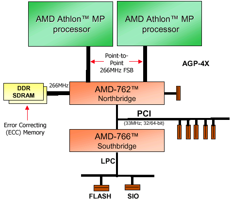
The other major difference is the PCI controller on the 762 North Bridge.
While the 761 North Bridge only had a 32-bit 33MHz PCI bridge, the 762 contains
a 32/64-bit 33MHz PCI bridge. This is the bus that connects the
Obviously, the support for only 33MHz 64-bit PCI is a limitation of the 760MP chipset; luckily, AMD does have something planned to fix this.


0 Comments
View All Comments