 |
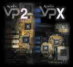
With the success VIA attained with the VP-1 and VPX chipsets it was time to drop a huge bomb on the competition by announcing a head to head competitor of Intel's latest and greatest TX chipset. VIA did just that with the announcement of the VP2/97 chipset, and it was that announcement that allowed them to gain the support of some of the industry's biggest names, including Advanced Micro Devices with the release of their AMD K6 Microprocessor. |
The VIA VP2/97 chipset combines the best features found in all Socket-7 chipsets, from BEDO and SDRAM support to UMA and UltraDMA support, the VP2/97 topples the competition with a rich feature set. The unique two chip solution from VIA packs a strong punch with, once again, a maximum of 512MB (all cached) RAM complimented by the large 2MB of L2 cache possible with the VP2/97. Supporting all processor classes from the early Pentium Classic to the Cyrix 6x86MX with support for Intel and Linear Burst Mode SRAM transfers the VP2/97 is truly a chipset for the masses.
Like Intel's TX chipset, the power saving features on the VP2/97 are tremendous which is a direct result of its PC97 compliance. The VP2/97 is in a class of its own since NO other Socket-7 chipset can even begin to support the features the VP2/97 boasts. The only downside to the VP2/97 is that it doesn't support AGP, which will be featured in the successor to the VP2/97, the VIA VP3 chipset.
| VIA VT82C590 Apollo VP2/97 Chipset | ||
| Common Name | Apollo VP2/97 | |
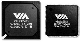
| Chipset Packaging | Number of chips | 2 (VT82C595 North Bridge, VT82C586B South Bridge) |
| Packaging Type | 1 x 328-pin BGA; 1 x 208-pin QFP | |
| CPU Support | Number of CPUs | 1 |
| AMD CPUs Supported | K5, K6 | |
| Cyrix CPUs Supported | 6x86 (M1), 6x86MX (M2) w/ Linear Burst Mode | |
| Intel CPUs Supported | Pentium, Pentium MMX | |
| Cache | Type | Synchronous Pipeline Burst Cache |
| Maximum Supported Size | 2048KB | |
| Maximum Cacheable DRAM Area | 512MB | |
| Memory | Maximum DRAM Supported | 512MB |
| BEDO DRAM Read Timings (66MHz) | 5-1-1-1 | |
| EDO DRAM Read Timings (66MHz) | 5-2-2-2 | |
| FPM DRAM Read Timings (66MHz) | 5-3-3-3 | |
| SDRAM Read Timings (66MHz) | 3-1-1-1 | |
| Data Path to Memory | 64-bits | |
| ECC Support | Yes | |
| Hard Disk Controller | Chip | VIA South Bridge Controller (VT82C586B) |
| Busmastering Support | Yes | |
| UltraDMA Support | Yes | |
| Max. Theoretical Transfer Rate | PIO Mode 5/DMA Mode 3 (33.3MB/S) | |
| PCI Interface | Supported PCI Bus Speeds | 25, 30, 33 MHz |
| Concurrent PCI | Yes | |
| Async. PCI Bus Speed | No | |
| PCI Specification | 2.0 (66 MHz max.) | |
| Power Management | PC97 Compliance | Yes |
| Suspend to Disk | Yes | |
| HDD Power Down | Yes | |
| Modem Wakeup | Yes | |
| System Suspend | Yes | |
| Video | AGP Support | No |
| Unified Memory Architecture | Yes | |
| Peripheral Support | USB Support | Yes |
| Plug and Play Port | Yes | |
| Write Buffers | CPU-to-DRAM | 16 QWords |
| CPU-to-PCI | 6 DWords | |
| PCI-to-DRAM | 48 DWords | |
| Officially Supported Bus Speeds | 50, 60, 66 MHz | |
| Unofficially Achieved Bus Speeds | 68, 75, 83.3 MHz | |


4 Comments
View All Comments
vortmax2 - Wednesday, June 25, 2014 - link
The good ole' days when you could put multiple vendor CPUs into the same motherboard. So simple...PentiumGeek - Thursday, September 1, 2016 - link
This motherboard was on my 1st PC. I was very disappointed when faced with the problem that DIMM and SIMM memory can't work in the same time. I used Pentium 100Mhz CPU on this motherboard :)Amadeus777999 - Wednesday, May 9, 2018 - link
Got an ASUS P2L97 board yesterday and I'm reading through this while DoomII is benchmarking. Good times.rogerjowett - Sunday, May 17, 2020 - link
Does n e 1 know where I can find a Voltage Regulation Module please