Computex 2011: ECS HQ Tour, Q&A and Booth
by Ian Cutress on June 11, 2011 1:55 AM EST- Posted in
- Computex 2011
- ECS
- Trade Shows
Despite being a motherboard reviewer, I’ve never had the chance to ever see inside the HQ of any of the prominent consumer and OEM motherboard vendors. Most of us decide which price and performance segment we want with our processor, and find a motherboard that fits the frame from reviews. There’s actually so much to designing and producing a motherboard that I didn’t realize before, so having a chance to see how ECS works and produces product from start to finish is one that I jumped at.
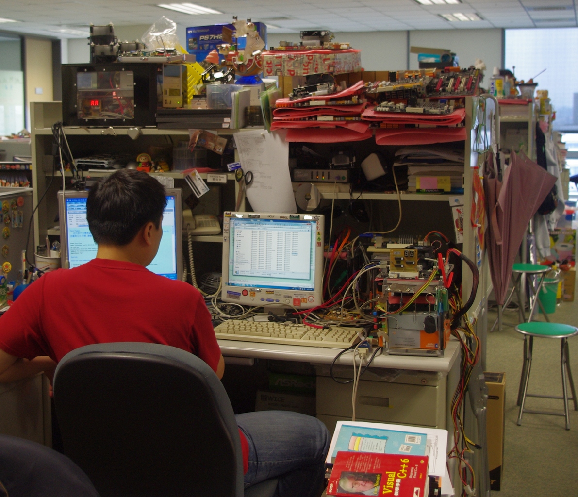
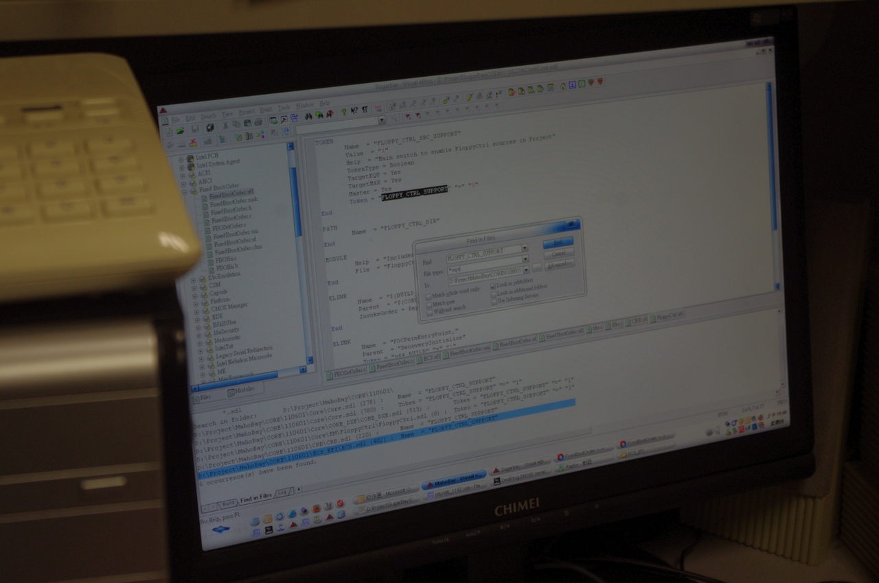
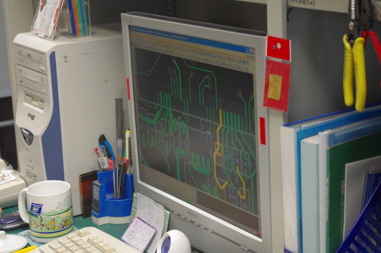
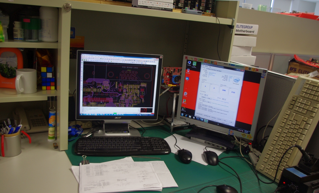
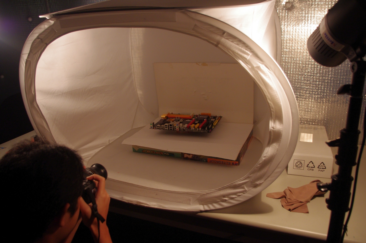
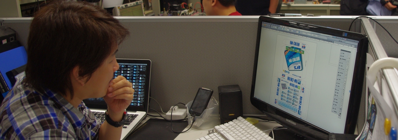
On floor 13 out of 20 of the ECS HQ in Taipei, I was shown one of the many research and design rooms at the motherboard manufacturer. In each cubicle were tens of motherboard products all being worked on by testers, BIOS coders, signal processors, trace designers, product marketers and so on. First, I was given a brief demonstration behind the motherboard product design from the engineer’s point of view. This in itself was interesting, going through the many stages of initial idea, to design, to testing, to debugging, and finally production:
-
Motherboard segments decided by product/project manager, often dictated by cost
- Discussions: Specifications, Schedule, Other Details
-
Schematic Design
- Data Research based on standards and chipset/IC specifications
- Initial schematic CAD design, checked and double checked
-
PCB Design
- Layer by layer – impedance for signal traces and signal integration
- Placement of components due to thermal, current and spatial consideration
- Layout as per design guidelines to avoid interference
- Initial PCB design in ECS factory
-
Motherboard Sampling
- Provide Bill of Materials
- Revision 0.1 PCBs from factory
-
Motherboard Testing and Debugging
- Complete test process – functionality, signal quality, power management, stability (3DMark), compatibility (software, games), electromagnetic disturbance testing
- Fix design errors by checking signals and reworking the design. Repeat as necessary
-
Motherboard Revision/Mass Production
- Revise all must-fix items and confirm all solutions are implemented
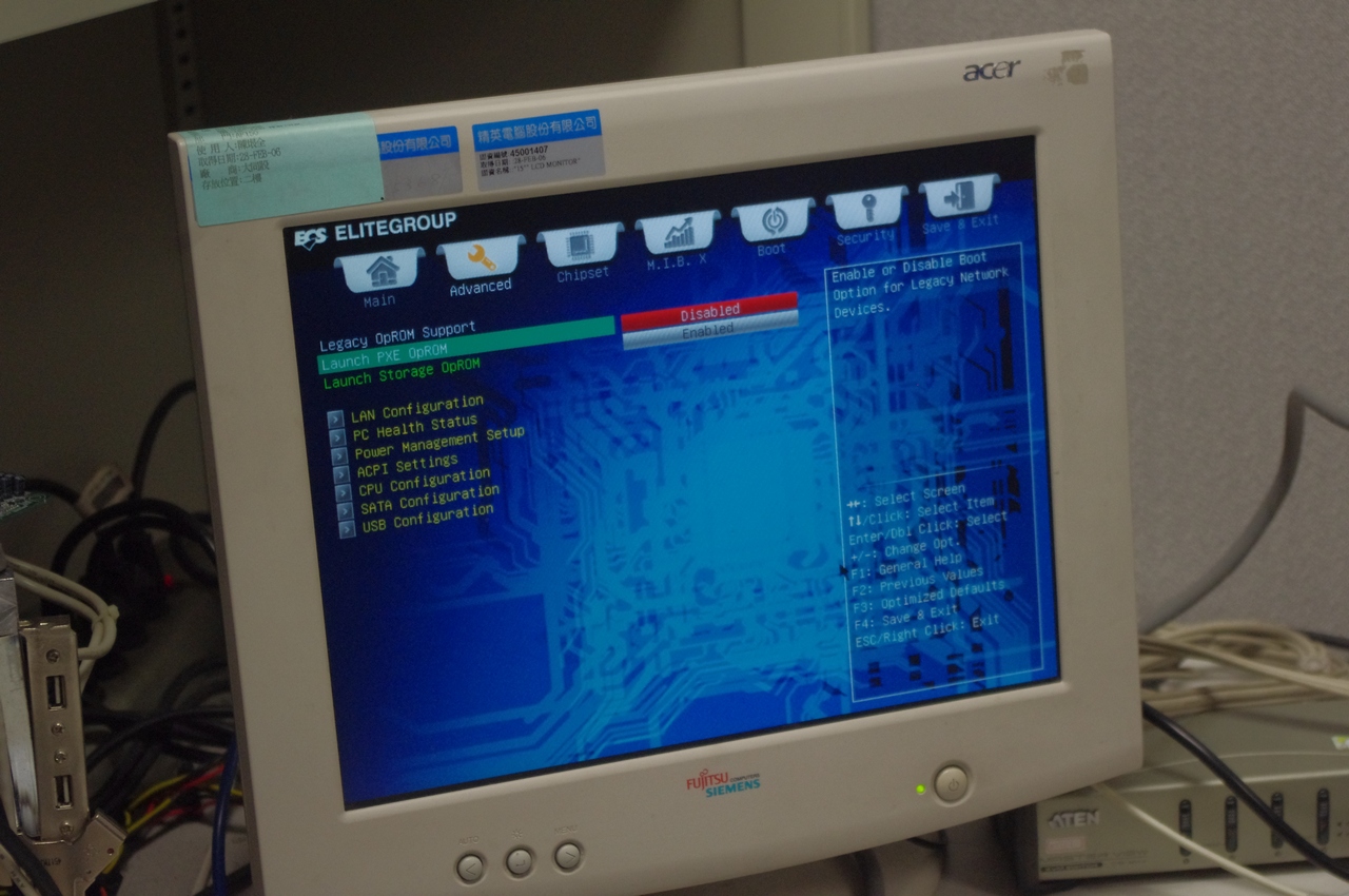
I was allowed to take an alarming amount of pictures whilst walking around the engineer’s cubicles, so I photographed anything and everything. For example we have BIOS engineers working on ECS’ new UEFI (out in July, apparently):
Power engineers working on trace lines:
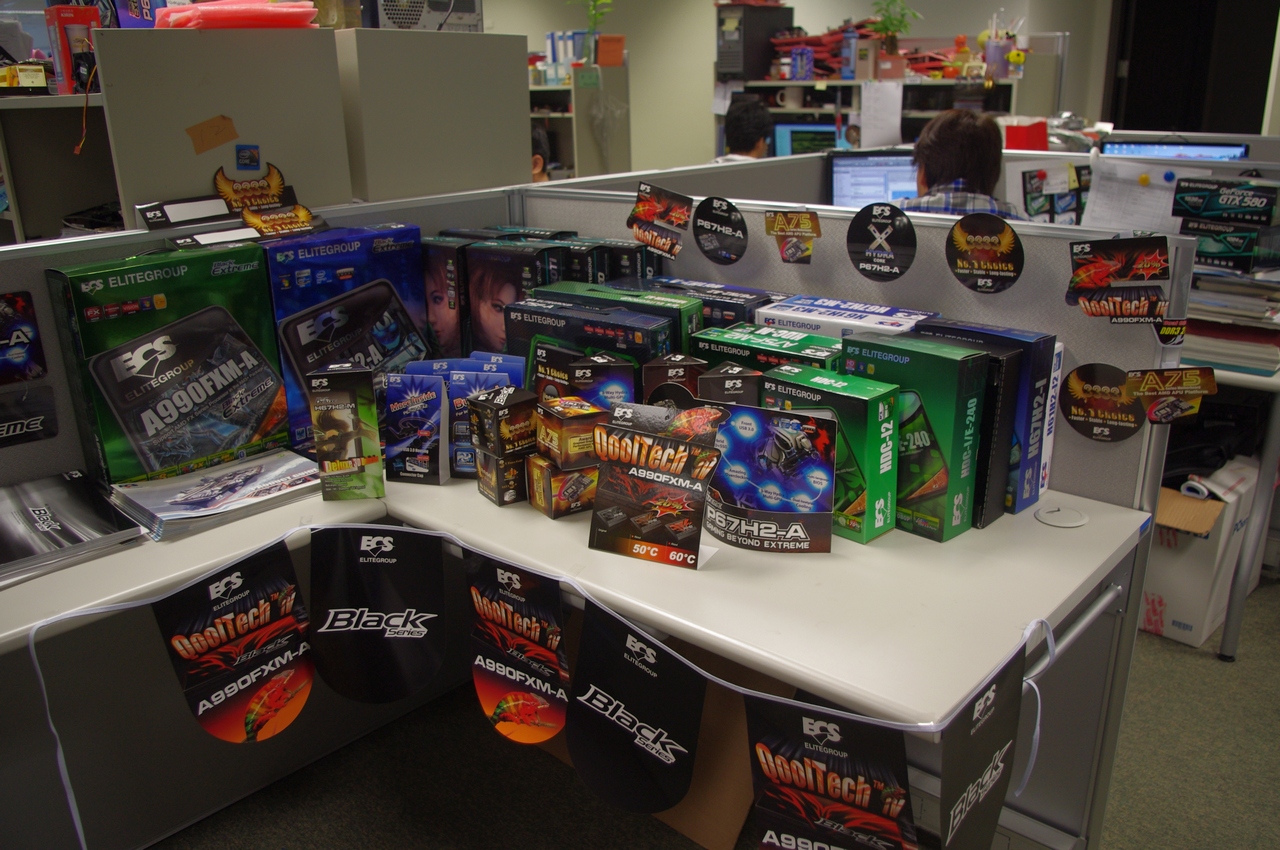
Designers working on the latest marketing and taking pictures of products:
And a variety of desks full of equipment and testing beds:


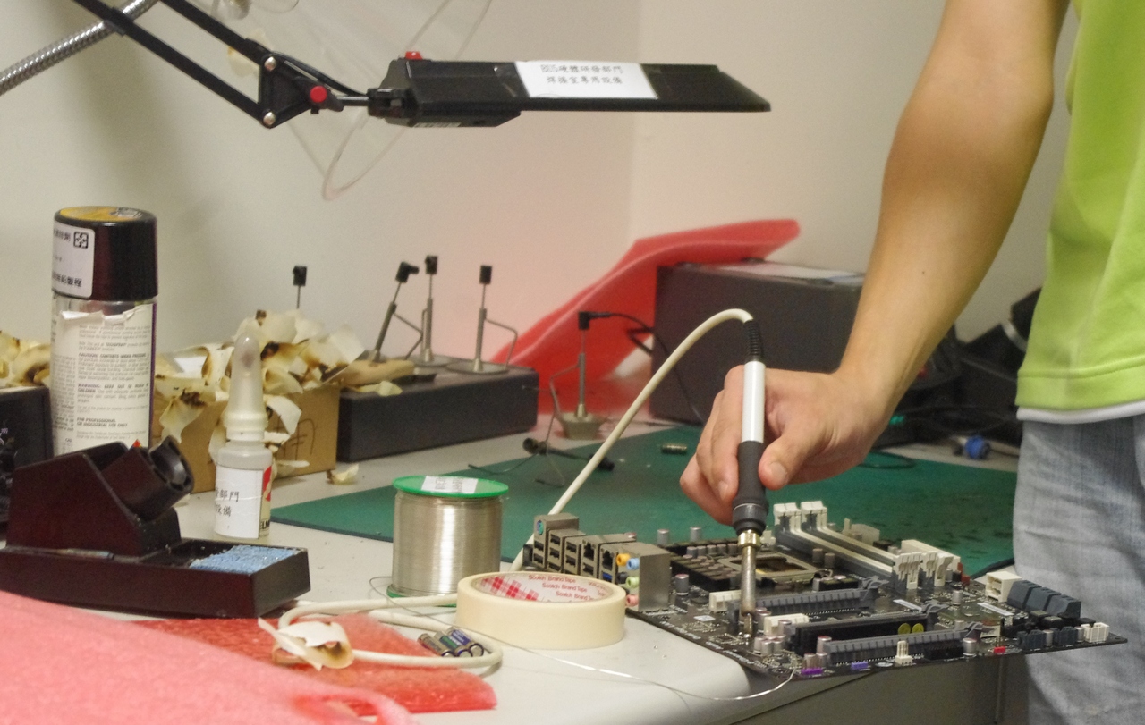
As part of the tour, the soldering room and oscilloscope testing were also shown:
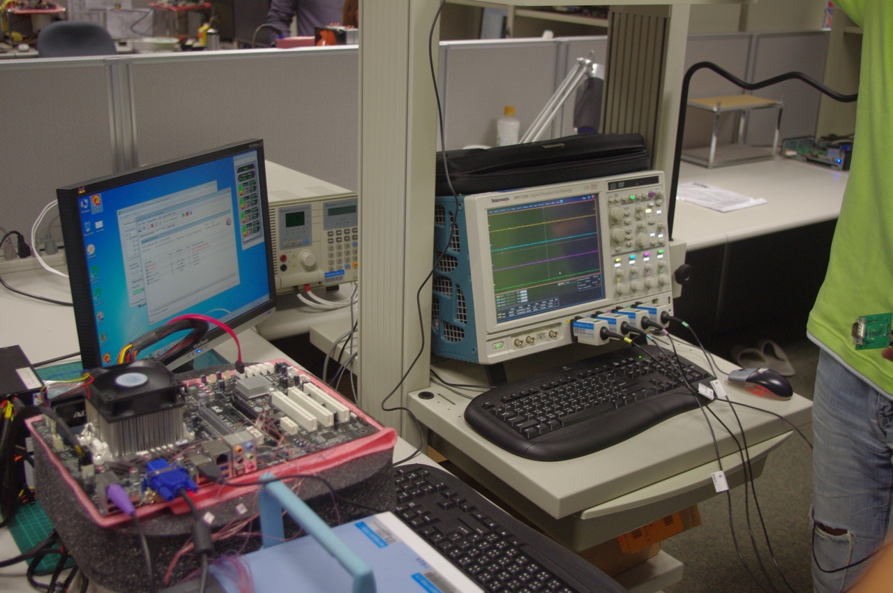
The oscilloscope was used for output signal testing – when the output is too high or low, the engineers will suggest changes to resistors and/or capacitors to improve the quality of the test PCBs.
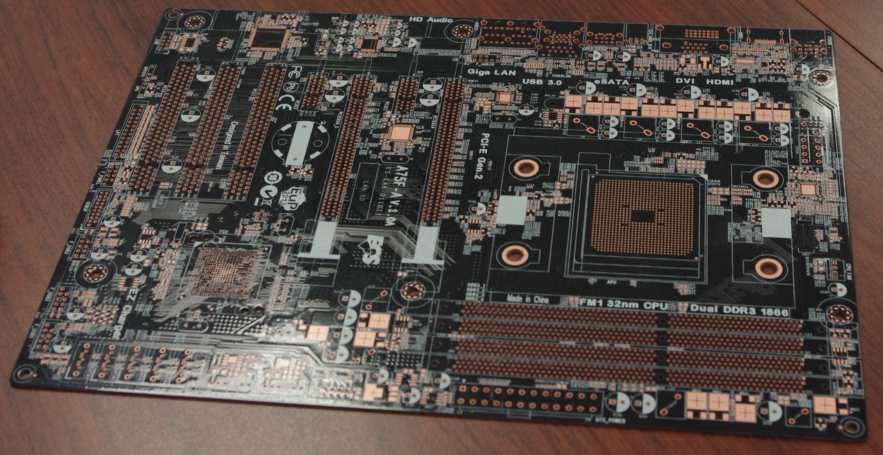
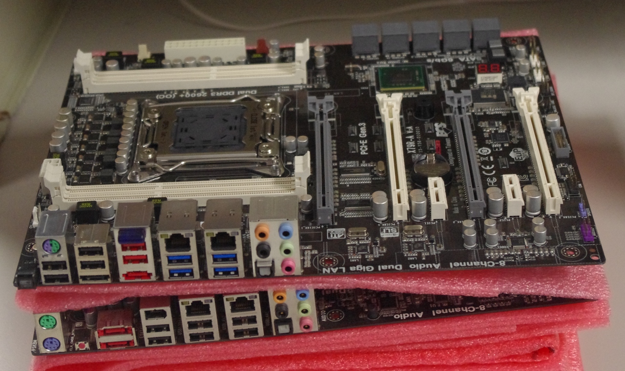
I managed to find an ECS X79R-A on one of the desks similar to what we’d seen at the booth, and took some pictures. This clearly shows that ECS are well on their way to an X79 product for launch – if I get one in to test I’ll let you know how it performs.


25 Comments
View All Comments
jigglywiggly - Saturday, June 11, 2011 - link
Here is our troll center where we ship defective products to consumers.StormyParis - Saturday, June 11, 2011 - link
I don't have quality issues with ECS boards. They're nice, basic ones. I actually quite like them: the lack of overclocking options prevents us from goofing with them. I had several issues with Asus boards.yyrkoon - Sunday, June 12, 2011 - link
Yeah I dont have problem with ECS either. Asrock on the other hand . . .Most of the people I repair systems for just want to cheap out, and in a lot of cases ECS has the least expensive boards around. Never had a problem with ESC like stability issues, or DoA boards. Like what can happened fro mthe two "A" company brands often enough for me to never put one of those boards in a personal system.
MSI also often has very reliable boards.
One more thing I have to mention. Is that "top performing" motherboards means very little, if that performance gap is tiny. Which is usually the case. 5-10% performance gap is only noticeable if you're bench marking. And, if that 5-10% performance gap means using an unreliable motherboard. That performance gaps means *nothing*.
My definition of reliable means that a system, with all it's components will run indefinitely without any issues pertaining to the hardware. That means, if the system soft resets, blue screens, etc EVER. That is what I consider unreliable. Many Asrock boards used to classify in this category. I could care less what features they have, how cheap the cost, and how well they perform.
ECS, if you're paying attention to the comments here. Keep up the good work, and please continue to give us a decently reliable product for a fair price.
Kim Leo - Saturday, June 11, 2011 - link
Omg I laughed so hard.. I have to agree, I've never had a good experience with ECS products. Supposedly they have improved, but it will be long while before I buy another ECS motherboard.Samus - Monday, June 13, 2011 - link
K7S5A was the best motherboard I've ever owned, and it has a SIS 735 chipset.The fact that ECS was able to extract that level of performance and stability from the 735 is remarkable. That was 10 years ago, too. It was even compatible with my fiberchannel Adaptec SCSI controller...which had boot problems in the Intel Intel 815e board I later put it in.
AssBall - Monday, June 13, 2011 - link
I have had good success with ECS motherboard builds too. They are reliable and don't have an excess of bullshit extras when you are building something simple and inexpensive, and easy to troubleshoot for friends and family who aren't enthusiasts.I think Ian criticized ECS fairly harshly considering how succesful they have been in an incredibly competitive market. It was a good article though and what a treat it would be to have a free tour of their Taipei offices.
I don't think a logo that changes color is a gimmick. I think it is kinda cool, and I thought I was the curmudgeon...
Oxford Guy - Sunday, June 12, 2011 - link
I've had two ECS motherboards. One of them, a really old RS-482M-754 is still in use. I didn't have problems with either of them. I don't know about the second board because I gave the system to someone I don't speak to anymore. But, the last time we did speak, which was several years after he had had the system, he said it worked fine.Just don't try to overclock them!
ChadnSteff - Saturday, June 11, 2011 - link
I'm with SHUD BE on this one. I'm not giving ECS another dime until people I know have received good products from them. The last few mobos I had from them were absolutely rubbish and their support was the pits. My friend who runs IT at the local university newspaper had similar experiences, and most of the hardware sites seem to need to be invited to these tours in order for any decent pr to be had. I'll stick with ASUS thanks.havoti97 - Saturday, June 11, 2011 - link
I bought an ECS video card, which promptly crapped out within the 3 year warranty period. Their customer support is a joke. I was directed to a broken RMA website. They never fixed nor replaced it. I would never spend another dime on the ECS brand.TemjinGold - Saturday, June 11, 2011 - link
Honestly, if ECS or any other motherboard/graphics card company wants more sales, what they need to do is to offer reliable products and stellar customer service. Bad service and poor word of mouth is what's killing these companies. If I hear about some revolutionary technology coming out from them, I would just read it and say, "Oh that's interesting." But if they want my money, I need to hear about awesome service.