Globalfoundries Starts on 22nm Fab & Announces First non-AMD Customer
by Anand Lal Shimpi on July 29, 2009 4:01 AM EST- Posted in
- CPUs
Maintaining Moore's Law
Every two years we need the ability to make chips smaller and cram more transistors into the same area. It makes microprocessors faster, more complex and cheaper depending on what you do to them. It also really helps with the whole ridiculous pace of innovation our industry likes to maintain.
If our ability to do that came to a halt, we'd be faced with our own little economic-depression in the microprocessor industry.
The threat that it will come to a halt is real, just as the confidence that we'll be able to innovate through for the next 10 - 15 years at least. It's all a matter of size. In order to cut transistor area in half every two years, you need to be able to physically design circuits that small - which requires some very expensive and precise equipment.
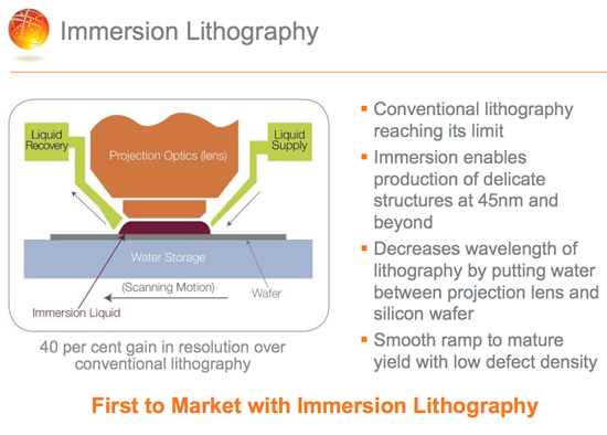
Hitting 45nm was difficult, but possible. AMD/Globalfoundries resorted to immersion lithography to make the transition. Basically it involves using liquid to improve the resolution of current 193nm lithography tools. By the time 32nm rolls around, Intel may have to do the same. Scaling beyond 32nm may reach the optical limitations of the current tools. Designing smaller, more densely packed chips may not be possible.
The replacement technology is something called extreme ultraviolet lithography. It's uses 13.5nm wavelength light (instead of 193nm) to be able to realize much finer patterns than current lithography tools.
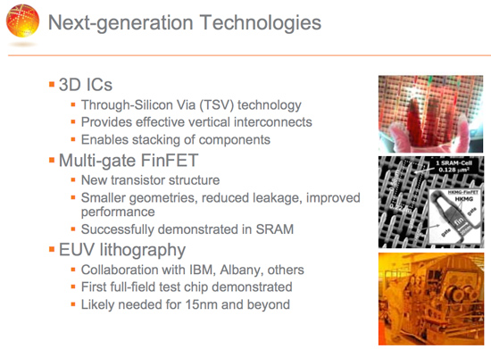
Multi-gate transistors are also expected to be needed at or after 22nm to maintain the sort of progress we've been used to. Multi-gate transistors are also non-planar so you can physically fit more in the same area, helping density issues.
Remember die-stacking? That's coming too.


50 Comments
View All Comments
drwho9437 - Saturday, August 8, 2009 - link
I think Anand is correct that FABs are ridiculously expensive and that the volume leader has a major advantage. However, it remains to be seen if the spin off is a good move for AMD.The honest truth is that 15 nm is probably the end of the road for gate lengths. That is a few generations away. Lithography can improve all you want it to, but leakage and process variability become more and more important as you go down in size. At 10 nm cube of Silicon has about 100,000 atoms in it. Even at 10^20 /cm^3 doping levels you are talking about 100 atoms in the channel. That's 10% variability in doping... 32 28 22 18 end of the road my friends. Of traditional Silicon that is. There really isn't anything right now to easily replace it, its just so nice chemically...
People will say the end has been predicted forever, and then claim I am wrong (at least that is what normally happens when I say this). I may be wrong but that isn't why. The sun comes up every day but one day it won't. One day we will hit the physical limits of Silicon and from my point of view it will be the statistical that will certainly be a problem. I think you'll see problems at around 10-15 nm.
What is exciting it the idea that we will have to finally be more cleaver than drawing smaller lines in Si and think of something truly original to make progress...
But given that that original idea may either take time to materialize or that it might be expensive, I think you will see reliable Si for a LONG time at some dimension. 40 or 32 nm may be with us a for decades in many types of systems... Given this, the cost of upgrading FABs may stop because there will be no more upgrades. Then you ask do you want control over them or not... I can see arguments on both sides. Certainly in the near future AMD had no choice cash flow wise.
There are other ways to innovate other than die shrinks, and leaning on optics and chemistry. We shall see if we are cleaver enough.
cosminliteanu - Monday, August 3, 2009 - link
Thank you for this article :)zodiacfml - Sunday, August 2, 2009 - link
Thanks Anand! Some good posted comments too.toyotabedzrock - Saturday, August 1, 2009 - link
$88M / 1,400 Jobs = $62,875. So a lot of the jobs must be for not highly skilled people? I consider highly skilled to be worth $80-100K.Doesn't the US control how much of our most advanced tech is exported to certain countries? We only just recently allowed Intel to build a 65nm fab in China.
drwho9437 - Saturday, August 8, 2009 - link
Typical FAB worker would probably hold a BS in EE, Chem, Mat Sci, starts at about 42-50K when I graduated undergrad. Those 10K slots add up for the MS/PhD who run the line or whatever.mesiah - Thursday, July 30, 2009 - link
Great article! I love reading stuff like this. I am by far not an expert in the field, but it sounds like EUV could revolutionize the chip making process. Although it looks like it still has a significant number of hurdles to overcome, especially when it comes to WPH. Also an exciting prospect but many more years off is the current research with graphene. Its hard to imagine the processing power we will be able to harness in the near future. Alot of people take for granted the devices we use today. Things like iphones and netbooks were hardly dreamed of when I was a kid. Sure, we talked about seeing stuff like this 15 years ago, but I guess I never believed it would happen so fast.MODEL3 - Wednesday, July 29, 2009 - link
Great article.I just have some questions regarding fab companies such TSMC:
Until 180nm, we had a very good tempo for manufacturing proccess transitions.
Then suddenly, from 180nm to 90nm there was a very profound deceleration.
Then from 90nm to 40nm (and for the medium-term future) we have an increase of the tempo again.
Why they keep increasing the tempo?
You said that the R&D cost increased dramatically and that the Fab Start-up Cost increased dramatically also. (I am not arguing, after all I don't have a technological background)
So if for a company such TSMC, the cost has increased so much more in relation with the past then it should charge their customers per wafers (per size counted in) much more, right?
Then Why between 90nm and 55nm:
The die size per price range increased exponentially (I have done the calculations with Nvidia chips because the "die information" was more easily found on the net)
This is a fact.
Unless that your explanation is simply that Nvidia & ATI made way way more money back then, or that TSMC was robbing Nvidia/ATI back then, what is your explanation?
I mean that, yes it is easy to figure out that Nvidia & ATI made more money back then, but the financial data does not support such a huge difference.
My guess (out of the conspiracy book) is that already exists a valid successor of silicon based type methods and they just milking the current technology (for the next 5-10 years)
(I am not talking about technologies to scale down lithography, like alpha EUV, I am talking about THE next step to silicon based types)
In another subject you said:
Note that this 28nm process is a “half-node” (between 32nm and 22nm) and where I’m expecting to see ATI (and NVIDIA) GPUs made at Globalfoundries"
Why are you expecting 28nm to be that process?
Do you think that after 28nm the TSMC will skip 22nm (like they did with 45nm) and focus on 20nm (so the transition will take them more time), so GF will find an opportunity to offer something competitive?
drwho9437 - Saturday, August 8, 2009 - link
High K and SOI both expensive gave new breathing room. But they both are stop gap measures... Bigger problems to come. Expect 32 nm and the next node to go OK then bigger fish enter the picture.Also don't expect way higher frequencies. 2 GHz is pretty easy to design. I can do a PCB that is flat to 2 GHz in about an hour... Designing in the X band however is painful.
Still all sorts of interesting things going on outside Si, organics, molecular switches, terahertz, optics on chips, the return of magnetic. They are all pain in the butt compared to better lithography though :-)
Zagor Tenay - Wednesday, July 29, 2009 - link
Great article! It is so relieving to see that the whole semiconductor industry is not a captive at the hands of an ugly, greedy beast called INTEL.Zingam - Wednesday, July 29, 2009 - link
Don't forget that AMD owns the GF. If GF makes a profit. AMD gets revenues.I don't think that AMD does not have foundries anymore. They are just not attached to it. It isn't the same as NVIDIA - they do not possess anything like GF.