DFI X48 LT T2R: Floats like a Butterfly…
by Rajinder Gill on April 28, 2008 4:00 AM EST- Posted in
- Motherboards
Toe to Toe with the BIOS (cont'd)
 |
 |
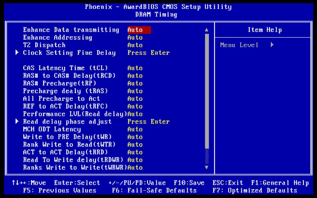
Regardless of individual memory timing preferences, to obtain best RAM/chipset latency performance we recommend that the following BIOS functions be set as follows for Micron D9-based RAM modules.
Enhance Data Transmitting: FAST
FAST MODE: Gives latency and bandwidth improvements over the "Normal" setting without overly affecting memory stability or FSB overclocking potential throughout the frequency ranges of interest for everyday use.
TURBO MODE: More suited to benchmarking runs. This is a very aggressive setting, further improving latencies past "Fast" mode. Using "Turbo" mode may require that the "CH1CH2 Common CLK Crossing Setting" be set to "Nominal" rather than "More Aggressive". VNB requirements are 1.7V and upwards, hence this should be used strictly for short-term benchmarking.
Enhance Addressing: FAST
This brings additional gains of latency and bandwidth used in combination with the above setting for best overall system performance. Again, the stability/voltage requirement hit is only minor for normal PC use. Although the BIOS defaults to Normal mode for both settings, there is no reason to veer away from setting FAST for both functions, provided you're using reasonable memory.
T2 Dispatch: Set this to Disabled, as it gives more overall stability when memory is clocked to high speeds.
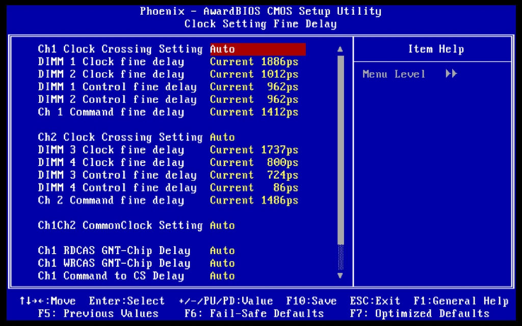 |
Channel 1 CLK Crossing Setting: More Aggressive
Channel 2 CLK Crossing Setting: More Aggressive
CH1CH2 Common CLK Crossing Setting: More Aggressive
24/7 systems using Micron D9GMH-based modules will certainly want to take advantage of using all three of these settings in unison for a latency and bandwidth boost. We have found these three functions set to "More Aggressive" do not hinder the boards FSB progress excessively. Other RAM modules may not fare as well, unfortunately. Given the choice between a hike in tRD (performance level) or setting the clock crossing settings less aggressively, always strive to maintain the lowest tRD possible. Taking a hit in the clock crossing setting is not as drastic as additional clock delays to the tRD transfer cycle.
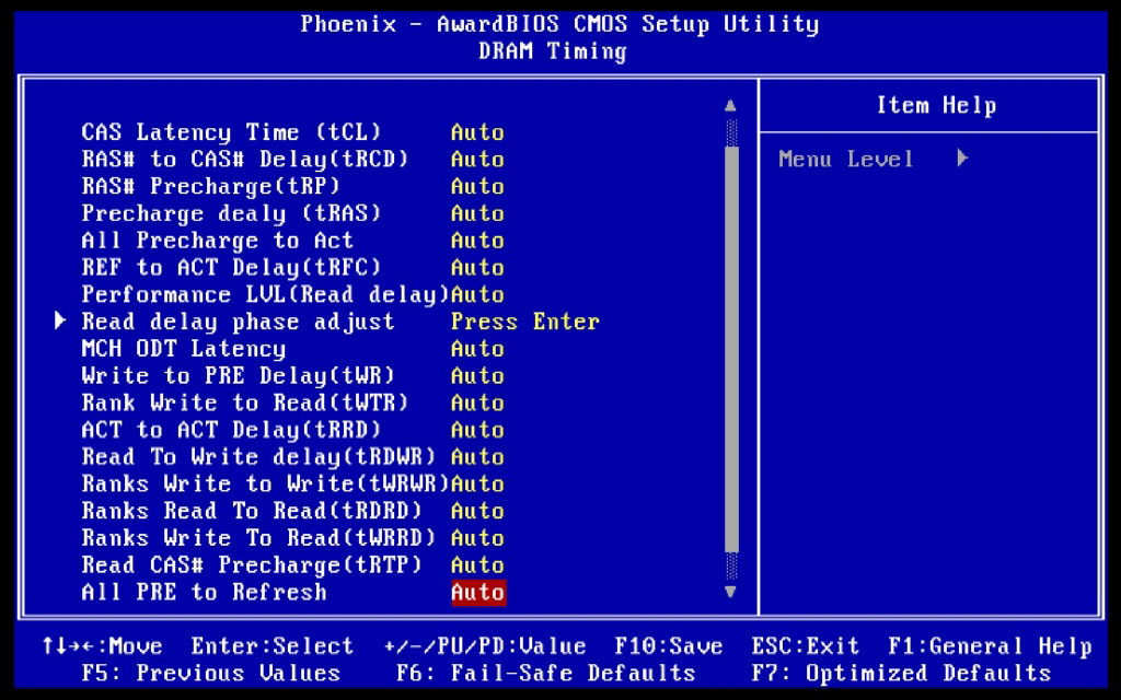
Clock Fine Delays: For both channels, the BIOS adjusts these values automatically when set to CURRENT mode. The scale runs in picoseconds of delay for each setting/channel. Generally, engineers do a very good job of ensuring PCB trace lengths to each DIMM slot on the motherboard are of equal length. Slot 4 is around 3 cm or so from slot 1, so the traces running to DIMM slot 1 will often be "snaked" back across themselves in a U shape to add length to the trace and help eliminate parasitic capacitance issues when running two traces in parallel. The delay functions offer adjustment to help eliminate trace length mismatches ensuring data requests from the MCH are received and dispatched in unison when requested from the appropriate DIMM banks.
Although the BIOS does an admirable job of sensing the delay values required, we found that pushing the board requires some manual tuning of these settings. The Control Fine Delay values for each channel can often be left at Current, while tuning the Clock Fine Delay and Command Fine Delay Settings for both channels is certainly fruitful (depending also on which DIMM slots are occupied by modules). For the most part the delay in picoseconds between each bank should not exceed 70ps or so. Command Fine Delay seems to function best when set to around a 50% value of Clock Fine Delay.
The best way to monitor these settings is to write down the values at default (Current), if the board is stable. As you increase the FSB and hence change the memory frequency, the current values tend to drift away from their ideal or stable settings. To get around this, users can manually apply the settings shown for a stable overclock and tune the board for better stability by making small adjustments to the manually applied values. Do note however, that the values shown by the current settings are not available in the manual adjustment scale, so we must pick the closest value.
At times, the BIOS may select a Command Fine Delay setting that is wholly inadequate for the frequency applied. Often a value under 100ps may be selected, resulting in the board failing to boot into the OS, simply setting this value back to near 50% of the Clock Fine Delay value of Channel 1&3 often results in a "fix".


24 Comments
View All Comments
orangeblue - Friday, June 13, 2008 - link
hi,can anybody tell me if the ocz flex 9200 4gb-kit(2x2048) workz too instead the four 1024 plz.
Zoomer - Saturday, May 3, 2008 - link
I miss the analysis of other features than just plain memory latency.Max fsb overclock, max mem overclock, etc?
Running the board at 400fsb seems boring - lots of P965 boards can best that. Tons of people don't buy these multiplier unlocked chips.
Rajinder Gill - Sunday, May 4, 2008 - link
Hi,Dual core 45nm's top out at around 510-515FSB using air cooling. Most of the quad CPU info is in the review.
We are looking at perhaps adding some more content tomorrow. Mainly 2x2GB and 4X1GB maxmimum stable overclocks and best operating points - using air cooling.
When Using 45nm dual core CPU's X48/X38 chipsets are really only 'good' to around 500FSB tops for 24/7, after this VMCH requirements and total stability with low tRD becomes futile rather quickly. SOme of the DDR3 boards are a little better in this regard, though this overhaed always comes at a high voltage price when used with a suitably high CPU multiplier.
65nm CPU's in dual core form may cruise upto 550fsb with some work, perhaps a 67% GTL table will help for that. Many of the benches in the review were run at 8x500FSB just to reflect the maximum 24/7 somebody is likely to be able to achieve and/or use consistently. FSB values over this are prone to failure in applications like PC Mark Vantage or 3D in some instance (even with lots of GTL work). Our E8500 processor managed 510FSB with 4X1GB maximum stable on this board, while using 2x1GB memory allowed me to boot at a around 520FSB - though this was far from being called stable.
regards
Raja
Zoomer - Wednesday, May 7, 2008 - link
Thanks for taking the time to respond.Unfortunately, I have not been keeping up with the latest tweaks on the best boards. Thanks for the detail, though. :)
amalinov - Friday, May 2, 2008 - link
Am I imaging things or something fishy is going on here?The board has 2 PCIe 2.0 x16 slots - from the X48 MCH. OK.
The board has the following PCIe devices connected to the ICH9R:
1. PCIe x1 slot
2. PCIe x1 JMB363 SATA/PATA controller
3. PCIe x1 Marvell 88E8052 Gigabit Ethernet controller
4. PCIe x1 Marvell 88E8053 Gigabit Ethernet controller
5. PCIe x4 slot (physical x16)
IMHO in this situation the x4 slot can be utilized as x4 only if at least 2 of the PCIe x1 devices are disabled? (if so, then wich exactly?) But this is not mentioned anywhere - neighter in the review, nor in the official DFI specifications or manual. Also, in the manual there is no BIOS settings description section - so I can't find what does the "PCIE Slot Config - 1X 1X" option stand for? (I assume for putting the x4/x16 slot in x1/x16 mode when the other devices are not disabled?)
n7 - Tuesday, April 29, 2008 - link
Great stuff.I have one concern though.
What are you using to test stability for 8 GB?
I have found that what people like to consider "stable" is only stable because of the use of applications like P95, Everest, OCCT, & Memtest86+, which don't tend to really stress 4+ GB RAM & the Northbridge to the same extent as multiple instances of HCI Memtest or as LinPack.
Just curious is all.
Rajinder Gill - Monday, May 5, 2008 - link
HCI memtest seems the way to go for me for memory NBGTL related stuff.For CPU core testing Prime/PC Mark Vantage (Blu-Ray test).regards
Raja
aldy402 - Tuesday, April 29, 2008 - link
great review RajinderIt was very in-depth and well written. A big chunk of the memory portion seemed to focus on micron D9 chips. I have the 4gb Gskill(powerchip ICs) and would really like to see a write up on this board involving "other ICs" and maby a guide with 65nm quads.
also have you tested the performance differential between the intel and jmicron sata ports?
well done
-Aldy
Rajinder Gill - Tuesday, April 29, 2008 - link
HI Andy,Although the guide says Micron I did add a comment on TRFC and double density modules. tRAS adn tRFC are the 2 tiimings that need to be changed for the most part. The boards will hold upto 450FSB and a dual core 45nm 'stable' with most of the chipset registers set to fast/more aggressive. Comments are already in the guide for 65nm CPU's pertaining to leaving the GTL controls at defaults - nothing more is really needed tbh..
regards
Raja
coolbluewater - Tuesday, April 29, 2008 - link
Replacing two of the six USB ports ith two eSata ports would seem to make sense. Not sure why they didn't do this on a board in this price range.