NVIDIA's GeForce 8800 (G80): GPUs Re-architected for DirectX 10
by Anand Lal Shimpi & Derek Wilson on November 8, 2006 6:01 PM EST- Posted in
- GPUs
The 680i Platform
Alongside the GeForce 8800 GTX and GTS, NVIDIA is launching a brand new chipset for Intel processors, the nForce 680i (and 650i SLI and Ultra). Our own Wesley Fink has published an in-depth look at the new chipset, but we felt the release significant enough to comment on some of its features here in this review.
For the most part, competing with Intel for its chipset business is an effort in futility. The companies that have tried have ended up either segregated to the low end of the market or kept to an extremely small niche. The past has proven that it is simply very difficult for a company that isn't Intel to produce a better performing chipset for Intel processors.
The multi-GPU era has changed things a bit, because now all of the sudden there's a new feature that Intel can't simply support on its chipsets. It took a while but ATI eventually allowed Intel to support CrossFire on its chipsets, but who knows how long that will last given ATI's new owner. While ATI caved in and supported Intel, NVIDIA would not capitulate. NVIDIA is like a mini-Intel and just like the big version, it doesn't play well with others. Licensing SLI for use on Intel chipsets was simply not in the cards; instead NVIDIA used SLI support as a reason for Intel users to consider NVIDIA chipsets. As NVIDIA continues to have the stronger multi-GPU lineup (although ATI has recently started fixing some of its problems with CrossFire), the SLI brand remains strong.
Although behaving like a veteran chipset manufacturer, NVIDIA is still a relative newcomer to the chipset business, but one thing we have seen from the boys in green is that they definitely learn from their mistakes. Dating back to the original nForce chipset, NVIDIA fell flat on its face with its first attempt at PC core logic, but bounced back to topple VIA with its nForce2 chipset. And it's that nForce to nForce2 transition that we're seeing here again with NVIDIA's nForce 680i SLI.
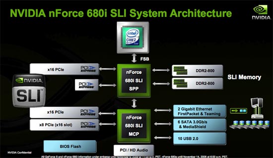
The 680i SLI is strictly a high end chipset, as the lower end of the market will still be serviced by NVIDIA's 570 SLI. The 680i supports all of the checkbox features: 1066MHz FSB (with unofficial support for higher speeds), dual channel DDR2-800, two PCIe x16 slots, one PCIe x8, 2 GbE ports, 6 SATA, 10 USB and HD Audio.
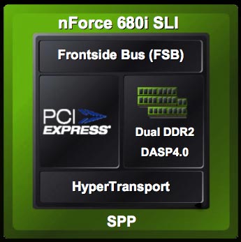
There are some pretty unique features about the new chipset. For starters it is the first NVIDIA core logic to be built on a 90nm process. The 680i SPP (aka North Bridge) is built on TSMC's 90nm process and thus ends up running cooler and can be overclocked more than NVIDIA's previous offerings in the area. The South Bridge (680i MCP) is still a 130nm chip but its functions are far less critical than those of the North Bridge.
In the 680i SPP is an updated version of NVIDIA's pre-fetching core called DASP. The major change to the 680i's DASP is that it is optimized for the memory access patterns of Conroe and Kentsfield which apparently are very different from NetBurst CPUs of the past. Given the aggressive prefetching done by the new Core processors and the large shared L2 cache, it isn't surprising to find out that memory controllers tuned to older Intel processors might not be best optimized for Core.
The primary function of the 680i's DASP is to examine memory access patterns and prefetch data into a local buffer that it thinks the processor will need at a later point in time. The updated version of DASP prefetches one cache line (64B) at a time into an internal buffer, although NVIDIA wouldn't disclose the size of the buffer.
We couldn't get much more information on DASP 4.0 from NVIDIA other than it supports prioritizing of reads over writes (to avoid read-to-write delays from random memory requests) and that a number of proprietary algorithms are used to make sure that prefetching doesn't occur when the CPU actually needs data from the memory controller.
Overclocking is a very large part of the new 680i chipset, and Wes' review of it goes into great detail about what exactly is possible with this new platform. For us, the other interesting part of the 680i platform is that, for the first time, NVIDIA is allowing its partners to sell NVIDIA engineered and designed 680i motherboards.
It has often been the case that a chipset maker's reference board has far more bells and whistles than anything its motherboard partners actually sell on the market. NVIDIA was growing weary of this being the case and instead effectively engineered a reference board that could be sold in retail.
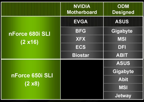
Motherboard makers can still choose to design their own 680i boards, but some have opted to simply rebrand NVIDIA's design.
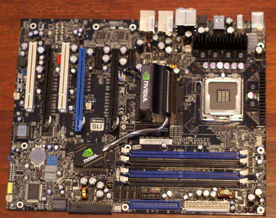
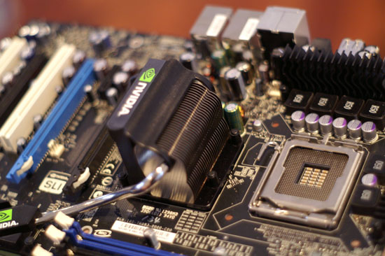
We ran all of our tests for this review on NVIDIA's nForce 680i SLI motherboard; this particular one is branded by EVGA. We were extremely pleased with the stability, BIOS, attention to detail and overall performance of the 680i solution. The decision to introduce NVIDIA designed 680i boards also shows how far NVIDIA has come as a manufacturer; if you want something done right, you sometimes have to do it yourself, and that's exactly what NVIDIA decided to do here. Honestly, the only downside is its estimated cost of $229.
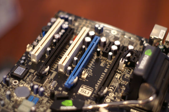
Three PCIe x16 slots (one is an x8 electrical)
NVIDIA is also introducing a lower cost 650i SLI chipset with only two x8 PCIe slots, but there will be no NVIDIA engineered boards available based on that chipset.


111 Comments
View All Comments
Nightmare225 - Sunday, November 26, 2006 - link
Are the FPS posted in this article, Minimum FPS, Average FPS, or Maximum? Thanks!multiblitz - Monday, November 20, 2006 - link
I enjoyed your reviews always a lot as they inclueded the video-capbilities for a HTPC on previous cards. Unfortunately this was this time not the case. Hopefully there will be a 2. Part covering this as well ? If so, it would be nice to make a compariosn on picture quality as well against the filters of ffdshow, as nvidia is now as well supporting postprocessing filters...DerekWilson - Tuesday, November 21, 2006 - link
What we know right now is that 8800 gets a 128 out of 130 on HQV tests.We haven't quite put together an HTPC look at 8800, but this is a possibility for the future.
epsil0n - Sunday, November 19, 2006 - link
I am not agree with this:"It isn't surprising to see that NVIDIA's implementation of a unified shader is based on taking a pixel shader quad pipeline, and breaking up the vector units into 4 scalar units. Now, rather than 4 pixel quads, we see 16 SPs per "quad" or block of stream processors. Each block of 16 SPs shares 4 texture address units, 8 texture filter units, and an L1 cache."
If i understood well this sentence tells that given 4 pixels the numbers of SPs involved in the computation are 16. Then, this assumes that each component of the pixel shader is computed horizontally over 16 SP (4pixel x 4rgba = 16SP). But, are you sure??
I didn't found others articles over the web that speculate about this. Reading others articles the main idea that i realized is that a shader is computed by one and only one SP. Each vector instruction (inside the shader) is "mapped" as a sequence of scalar operations (a dot product beetwen two vectors is mapped as 4 MUD/ADD operations). As a consequence, in this scenario 4 pixels are computed only by 4 SPs.
DerekWilson - Tuesday, November 21, 2006 - link
Honestly, NVIDIA wouldn't give us this level of detail. We certainly pressed them about how vertices and pixels map to SPs, but the answer we got was always something about how dynamic the hardware is able to dynamically schedule the SPs optimally according to what needs to be done.They can get away with being obscure about how they actually process the data because it could happen either way and provide the same effect to the developer and gamer alike.
Scheduling the simultaneous processing one vec4 MAD operation on 4 quads (16 pixels) over 4 groups of 4 SPs will take 4 clock cycles (in terms of throughput). Processing the same 16 pixels on 16 SPs will also take 4 clock cycles.
But there are reasons to believe that things happen the way we described. Loading components of 16 different "threads" (verts, pixels or whatever) would likely be harder on the cache than loading all 4 components of 4 different threads. We could see them schedule multiple ops from 4 threads to fill up each block of shaders -- like computing 4 consecutive scalar operations for 4 threads on 16 SPs.
At the same time, it might be easier to maximize SP utilization if 16 threads were processed on one block of SPs every clock.
I think the answer to this question is that NVIDIA knows, they didn't tell us, and all we can do is give it our best guess.
xtknight - Thursday, November 16, 2006 - link
This has been AT's best article in awhile. Tons of great, concise info.I have a question about the gamma corrected AA. This would be detrimental if you've already calibrated your display, correct (assuming the game heeds to the calibration)? Do you know what gamma correction factor the cards use for 'gamma corrected AA'?
DerekWilson - Monday, November 20, 2006 - link
I don't know if they dynamically adjust gamma correction based on monitor (that would be nice though) ...if they don't they likely adjusted for a gamma of either (or between) 2.2 or 2.5.
Also, thanks :-) There was a lot more we wanted to pack in, but I'm glad to see that we did a good job with what we were able to include.
Thanks,
Derek Wilson
bjacobson - Sunday, November 12, 2006 - link
This comment is unrelated, but could you implement some system where after rating a comment, on reload the page goes back to the comment I was just at? Otherwise I rate something halfway down and then have to spend several seconds finding where I just was. Just a little nuissance.Thanks for the great article, fun read.
neo229 - Friday, November 10, 2006 - link
This is a very suspect quote. A card that requires two PCIe power connectors is going to dissipate a lot of heat. More heat means there must be a faster, louder fan or more substantial and costly heat sink. The extra costs associated with providing a truly quiet card mean that the bulk of manufacturers go with the loud fan option.
DerekWilson - Friday, November 10, 2006 - link
If manufacturers go with the NVIDIA reference design, then we will see a nice large heatsink with a huge quiet fan.Really, it does move a lot of air without making a lot of noise ... Are there any devices we can get to measure the airflow of a cooling solution?
We are also seeing some designs using water cooling and theres even one with a thermo-electric (peltier) cooler on it. Manufacturers are going to great lengths to keep this thing running cool without generating much noise.
None of the 8 retail cards we are testing right now generate nearly the noise of the X1950 XTX ... We are working on a retail roundup right now, and we'll absolutely have noise numbers for all of these cards at load.