RAM - Memory Technology Overview
by Jarred Walton on September 28, 2004 12:05 AM EST- Posted in
- Memory
Features and Design Considerations
We now have a pretty good idea of how memory is accessed, but there are a couple of other topics that are important, which we would like to address. In an ideal world, we would want high bandwidths, low latencies, low costs, and we want it all now. Naturally, all of these goals are in opposition to each other. It is possible, for instance, to create memory that offers both high bandwidth and low latencies, but the cost is considered prohibitive. One item that we have not addressed yet that bears mention is the complexity factor. It is a topic that companies can spend a lot of money examining.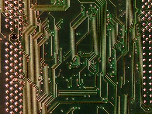
A faster memory interface that is very difficult to work with may end up getting scrapped, or at least delayed. For instance, dual-channel DDR configurations sound better in theory, but the difficulty of routing all of the traces between the RAM slots and the memory controller may not be worth the increased performance. Instead of using four layers in a motherboard or graphics card design, six layers or even eight may be required. Boards with more layers cost more money and more time to produce. Another factor is that in order to make all of the signals on each trace (wire) on the board arrive at the same time, they should be the same length. This requirement can lead to the "serpentining" of traces - a trace that zigzags back and forth in order to make it longer - as you can see in the above image. Testing and validation of motherboards become increasingly difficult as the number of traces and layers increase. Needless to say, determining the optimal configuration for a board design can be a very difficult balancing act.
With increasing clock speeds, signal integrity and interference also become more of a concern. Several trends have been at work lately, and not all of them are desirable. The first is that memory speeds have been increasing. This is desirable, but there are some drawbacks. In order to avoid signaling problems, we have gone from seeing eight RAM modules per memory channel to four modules, and now configurations that only support two modules are common. While DRAM density has been increasing, the reduction in the number of modules has worked against increasing the total memory size. In the server market, where large amounts of RAM are more important than having the fastest memory timings, technologies such as registered memory have helped to combat this. Future plans to help increase RAM size and speed without compromising the signal integrity include the switch to point-to-point connections instead of multi-drop busses, modified signaling algorithms that help to reduce interference, and on-chip signal termination.
As processor speeds increase, it is inevitable that memory performance will also need to improve. Manufacturing technologies have also improved, and so designs that were once too complex may become realizable in the future. Suffice it to say that memory manufacturers are not sitting idle, and there are designs and plans to help meet the increased demands of the future. We will be providing a more detailed look at the various options in the next article. For now, that covers the overview of the basics, and we can now get into some of the deeper details of memory performance.


22 Comments
View All Comments
666an666 - Thursday, May 14, 2009 - link
Thanks for the details. Unfortunatelt, most sellers of RAM (and most brand packagings) fail to mention these measurement details. They only show obscure model numbers and "PC-3200" or whatever. They usually only offer the choice of various brands, not various CL values.letter rip - Saturday, December 25, 2004 - link
This is great reading. When's the next installment?Herm0 - Wednesday, November 10, 2004 - link
There are two things that sould improve greatly a DIMM performance, in addition to the well known timings things "2-2-2-6"... , but looking at DIMMs specs, are hard to know :- The number of internal Banks. When a DIMM use multiple banks, the DIMM is divided in pieces, each holding its own grid of data and the logic to access it. Going from one bank to another one have no penalty : the memory controller have to send the bank address on two physical DIMM pins (so that it can't be more than 4 banks in a DIMM) at each access. Having a 2/4 bank DIMM is really like having 2/4 DIMMs : while one bank is waiting for a delay to exhaust (a CAS latency, a RAS latency, a RAS precharge...), the memory controller can send an order or do r/w things on another one... Most manufacturer build 2 banks DIMMs (when they publish that information !), few of them do 4 banks DIMMs.
- The wideness of their row. It's slow to access to the 1st data of a row (1: wait for tRP, Row Precharge, from the last operation, 2: send the new row address and wait tRCD, 3: Ras to Cas Delay, send the column address and wait tCL, Cas delay, read the 1st 64bit bloc of data), but it's fast to read from the activated row (Send the starting column and wait tCL, then read/write data, 1 or 2 per clock (SDRAM or DDRAM), of the pre-programmed length & order). In a ideal DIMM having only 1 row, the only penalty would be from the tCL one ! The more large is a row, the more data can be accessed before dealing with Row delays (Precharge, and Ras to Cas). The row size is nearly never published, and I don't know how to get the number from the detailed DIMM/DRAM specs...
Looking at 1Gb DDR400 DIMM modules too as #19, a good one, theorically, seems to be a Kingston's DIMMs :
- Timings = 2.5-3-3-7 (shouldn't last digit be 2.5+3+2 = 7.5 or 8 ?), most 1 Gb DIMMs are 3-3-3-8 or slowers.
- Banks = 4, most of DIMMs, even high-end ones, are only 2 Banks.
- Row size = ??? Unknown...
Am I right, or do I have to re-do Ars Technica lessons ? :-)
Gioron - Thursday, September 30, 2004 - link
In terms of buying 512M of fast memory of 1G of slow memory... here's what a quick look at prices for memory looked like (all corsair sticks and only from one vendor because I'm lazy and didn't want to complicate things):512M "Value" (CL2.5): $77
512M "XMS" (CL2): $114
512M "Xtra low" (2-2-2-5): $135
1G "Value" kit (CL3, 2x512M):$158
To me, it looks like the "Xtra low" is indeed not a good bang for the buck, with the 1G upgrade only $20 more. However, the "XMS" 512M might be a good price point if you don't want to go all the way to $158 but have more than $77. Going for insanely low latencies seems to be only worth it if you have plenty of cash to spare and are already at 1G or more. (Or else are optimizing for a single, small application that relies heavily on RAM timings, but I don't think you'll run into that too much in a desktop environment.)
One thing that might be useful in later articles is a brief discussion on the tradeoffs between size and performenace in relation to swapping pages to disk. Not sure if that will fit in with the planned article content, however.
JarredWalton - Wednesday, September 29, 2004 - link
??? I didn't think I actually started with a *specific* type of RAM - although I suppose it does apply to SDRAM/DDR, it also applies to most other types of RAM at an abstract level. There are lots of abstractions, like the fact that a memory request actually puts the row address and column address on different pins - it doesn't just "arrive". I didn't want to get into really low-level details, but look more at the overall picture. The article was more about the timings and what each one means, but you have to have a somewhat broader understanding of how RAM is accessed before such detail as CAS and RAS can really be explained in a reasonable manner.Lynx516 - Wednesday, September 29, 2004 - link
Not much has changed fundementaly with SDRAM since the early days of ddR.I never actually said a burst was a column but infact a continous set of columns (unless interleaved).
Ok I admit there arnt many books on processor design and latency however there are data sheets and articles that describe the basics. Once tyou have grasped the basics you can work it out using the data sheets e.t.c
Probably a better place to start with this series would have been the memory heirarchy instead of starting with a specifc
type of RAM
JarredWalton - Wednesday, September 29, 2004 - link
The idea here is to have an article on Anandtech.com. :) I like Ars Technica as much as the next guy, but there are lots of different ways of describing technology. Sometimes you just have to write a new article covering information available elsewhere, you know? How many text books are there on processor design and latency? Well, here's another article discussing memory. Also worth noting is that Ars hasn't updated their memory information since the days of SDRAM and DDR (late 2000), and things certainly have changed since then.I should clarify my last comment I made: the column width of DDR is not really 32 bytes or 64 bytes, but that seems to be how many memory companies now refer to it in *layman's* terms. This article is much more of a layman's approach. The deep EE stuff on how everything works is more than most people really want to know or understand (for better or for worse). A column can also be regarded as each piece of a burst, which is probably the correct terminology. We'll be looking at various implementations in the next article - hopefully stuff that you haven't read a lot about yet. :)
greendonuts3 - Tuesday, September 28, 2004 - link
Meh. You kind of started in the middle of the topic and worked your way outward/backward/forward. As a general user, I found the wealth of info more confusing than helpful in understanding ram. Maybe you could focus just on timing issues, which seems to be your intent, and refer the reader to other articles (eg the Ars one mentioned above) for the basics?Thanks.
JarredWalton - Tuesday, September 28, 2004 - link
The comparison with set associativity is not that bad, in my opinion. What you have to remember is that we would then be talking about a direct-mapped cache with a whopping four entries (one per sense amp/active row). I guess I didn't explain it too well, and it's not a perfect match, true.Regarding burst lengths, each burst is not a column of information, although perhaps it was on older RAM types. For instance, the burst length of DDR can be 4 or 8. Each burst transmits (in the case of single-channel configurations) 64 bits of data, or 8 bytes. The column size is not 8 bytes these days, however - it is either 32 bytes or 64 bytes on DDR. (Dual-channel would effectively double those values.)
ss284 - Tuesday, September 28, 2004 - link
I wouldnt say that the article is that confusing, but there is much truth in the post above^^^.-Steve