With the advent of RAID arrays, Gigabit Ethernet and other high bandwidth
devices on consumer class systems, PCI's 133MB/s available bandwidth is clearly insufficient to handle these demands.
Chipset makers have foreseen this limitation and have made various changes to
motherboard chipsets in order to alleviate some of the load from the PCI bus.
Up until 1997, graphics data was probably the single largest cause of traffic on
the PCI bus. The Accelerated Graphics Port (AGP), introduced by Intel's 440LX
chipset, had two main purposes: to increase graphics performance and to pull the
graphics data off the PCI bus. With graphics data transfers taking place on
another "bus" (technically, AGP is not a bus, since it only supports one
device), the previously saturated PCI bus was freed up for use with other
devices.
Yet AGP was just one step in reducing the load on the PCI bus. The next was to
redesign the link between the North Bridge and South Bridge of motherboard
chipsets. Older chipsets, such as the Intel 440 series used a single PCI bus to
connect the North Bridge to the South Bridge. The PCI bus not only had to cope
with inter-bridge traffic, but it also had to carry regular PCI traffic, IDE,
Super I/O (Serial, Parallel, PS/2), and USB. To alleviate the situation Intel,
VIA and SiS replaced the PCI bus between the North and South Bridges with a High
Speed interconnect, and then shifted IDE, Super I/O and USB to their own
dedicated links to the South Bridge.
Now with Intel's Communications Streaming Architecture bus built into the Memory
Controller Hub of the i875/i865 chipsets, even Gigabit Ethernet is off the PCI bus.
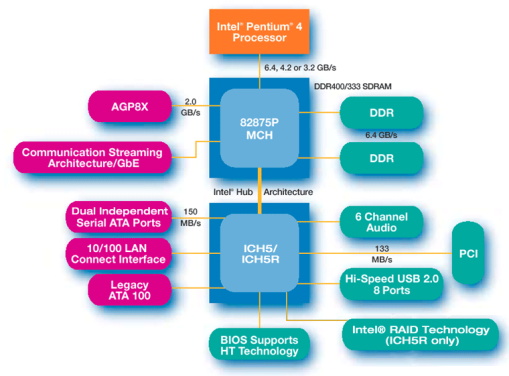
Numerous dedicated interconnects for various devices in the i875 chipset: not really a cost effective solution
While AGP, CSA, Intel's Accelerated Hub Architecture Hub Link, VIA's V-Link and SiS' MuTIOL have been relatively successful in reducing the PCI bus load, those are just stop-gap solutions.


3 Comments
View All Comments
Anonymous User - Saturday, September 20, 2003 - link
The demo board is a BTX - ATX's successor: http://www.anandtech.com/showdoc.html?i=1876&p...Anonymous User - Thursday, September 18, 2003 - link
First, for AGP, the official document about PCI-Express states that it can coexist with AGP. You must know that the PCI Express will only replace the PCI standard, so we can presume that the first board shipping with PCI Express will also ship with AGP.The PCI Express should not require any changes on power supplies, since it can go to lower voltages. I haven't read any technical spec, but it seems to be using some voltage-selection mechanism very similar to what is being used in USB devices (which did not require any power-supply mods).
Finally, for the form factor... well, I admit that I dunno. Form what I have read, no form factor mod should be necessary, but the demo board confuses me!
CYA!
Anonymous User - Thursday, September 18, 2003 - link
the transition from PCI to PCI Express won't happen overnight. ISA slots had stuck around for nearly 10 years before they were finally gone, so don't assume that your PCI peripherals are obsolete just yet.Thats very nice. But how about my brand new fancy AGP graphics card? I assume that purchasing a PCI-express motherboard also forces me to buy a new videocard.
Also when looking at the Intel layout demoboard I assume that there will also be a change in form factors and possibly also in power supplies. This means that all current cases would be obsolete then...
I realy enjoy the things that are going to happen in 2004 to the PC marked though! It's a real revolution again.