nForce2 6-way Motherboard Roundup - December 2002
by Evan Lieb on December 4, 2002 6:53 PM EST- Posted in
- Motherboards
Chaintech 7NJS: Stress Testing
1. Chipset and motherboard stress testing was conducted by running the FSB at 190MHz.
2. Memory stress testing was conducted by running RAM at 333MHz and 400MHz with as many modules populated as possible at the most aggressive timings possible.
Front Side Bus Stress Test Results
At 190MHz FSB, the Chaintech 7NJS had to go through an intensive amount of stress tests just as all the other nForce2 motherboards had to. We began with 24 hours straight of Prime95 torture tests running in the background. In the foreground we had our gaming suite running as well and after that was completed we headed onto general application performance and stability tests with light apps like Word and Excel, and eventually heavier loads like data compression and so on. We also reran a couple more stressful benchmarks like SPECviewperf, XMPEG and Sciencemark. In the end, it was clear that the 7NJS was very reliable at 190MHz FSB, as it didn't fail any of the stress tests we just mentioned.
Memory Stress Test Results
The consistently with which nForce2-based motherboards can operate three memory modules running at 333MHz DDR at the most aggressive possible timings is very impressive. Here were the timings we were able to achieve:
|
Stable
DDR333 Timings |
|
|
Clock
Speed:
|
166MHz
|
|
Timing
Mode:
|
N/A
|
|
CAS
Latency:
|
2
|
|
Bank
Interleave:
|
N/A
|
|
Precharge
to Active:
|
2T
|
|
Active
to Precharge:
|
4T
|
|
Active
to CMD:
|
2T
|
|
Command
Rate:
|
N/A
|
These aggressive timings cannot be matched by anything but an nForce2 motherboard. The Chaintech 7NJS is, not surprisingly, easily able to handle this DRAM settings. Remember, the CPU interface BIOS option is enabled at Aggressive as well, so we squeezed out the best performance we could in this DDR333 situation.
Our final DRAM stress test gauges the ability of the 7NJS to three modules at the best possible timings as high as possible up to 400MHz. Here were the timings we were able to achieve:
|
Stable
DDR400 Timings |
|
|
Clock
Speed:
|
200MHz
|
|
Timing
Mode:
|
N/A
|
|
CAS
Latency:
|
2
|
|
Bank
Interleave:
|
N/A
|
|
Precharge
to Active:
|
2T
|
|
Active
to Precharge:
|
4T
|
|
Active
to CMD:
|
2T
|
|
Command
Rate:
|
N/A
|
Now this is worth noting, mostly because not all the nForce2 motherboards were able to handle three modules running at 400MHz at CAS 2-2-2-4. Chaintech certainly did a fair job with the implementation, so we can be glad of that. Eventually, when the Athlon XP moves to a 400MHz FSB, you'll be able to take advantage of all this bandwidth (assuming you don't overclock).
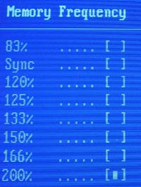
Memory overclocking turned out to be fairly impressive for the Chaintech 7NJS (at least compared to the nForce2 competition that is). Here were our results.
|
Stable
Memory Overclocking Results |
|||
|
Memory
|
Memory
Clock
|
FSB
|
VDIMM
|
|
Corsair
CAS2.0 DDR400
|
418MHz
|
157MHz
|
2.6V
|
As usual, we ran several memory stress tests and general apps to make sure these DRAM timings and frequencies were stable. We started off by running Prime95 torture tests; a grand total of 24 hours of Prime95 was successfully run at the timings and speeds listed in the above charts. We were also able to run Sciencemark (memory tests only), Super Pi tests and XMPEG encoding successfully while Prime95 was crunching away in the background. All in all, the Chaintech 7NJS proved reliable during all our memory tests.


1 Comments
View All Comments
c627627 - Monday, July 21, 2003 - link
MSI contradicts your reviewhttp://www.anandtech.com/mb/showdoc.html?i=1759&am...
You say:
"12/04/02 UPDATE: MSI sends word that the K7N2-L indeed does not have a PCI bus lock at 33MHz."
To this day, that was used as ultimate proof that the original MSI nForce2 mobo does not have a PCI lock.
Today MSI Senior Moderators said:
"they are wrong,and who ever told them it did not from msi"
(!)
Source:
http://www.msi.com.tw/program/e_service/forum/thre...
Won't you please settle this for us.