Original Link: https://www.anandtech.com/show/2911
NVIDIA Introduces dual Cortex A9 based Tegra 2
by Anand Lal Shimpi on January 7, 2010 2:00 PM EST- Posted in
- Smartphones
- Mobile
A month ago NVIDIA shared this slide with me:
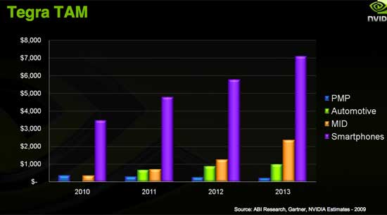
It's a graph of the total available market, according to NVIDIA, for its Tegra SoC (System-on-Chip). This year alone NVIDIA estimates that there's around a $4B market for Tegra. Next year it grows to $6B. By 2013 the total available market for NVIDIA's Tegra SoC reaches over $10B. That's more money than NVIDIA ever made from the PC market.
In order to compete in that space you need a competent chip. Today NVIDIA is announcing its second generation Tegra SoC. It's creatively named the Tegra 2 and this is what it looks like in block diagram form:
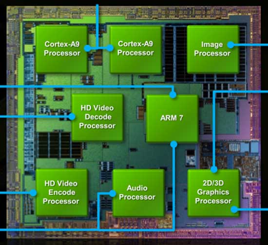
The SoC is made up of 8 independent processors, up from 7 in the original Tegra. The first two are the most exciting to me - a pair of ARM Cortex A9 cores. These are dual-issue out of order cores from ARM running at up to 1GHz. If you thought the A8 was fast, these things should be much faster.
The original Tegra used a single ARM11 core. It was multi-core capable but the only version NVIDIA ever shipped only had a single ARM11. By now you know that ARM11 is unreasonably slow and thus you see my biggest problem with Tegra 1. Tegra 2 addresses this in a grand way. NVIDIA skipped over Cortex A8 entirely and went to what it believes is a more power efficient, higher performing option with the A9. I'll go deeper into the A9's architecture shortly, but to put it bluntly - A8 is dead in my eyes, Cortex A9 is what you want.
The next processor is an audio decode core. NVIDIA acquired PortalPlayer in 2007 for somewhere around $350M. PortalPlayer SoCs were used in the first five generations of iPods. PortalPlayer contributed to much of NVIDIA's know how when it came to building SoCs and audio decoders. NVIDIA is particularly proud of its audio decode core, claiming that it can deliver system power in the low 10s of mW while playing an MP3. It's difficult to quality that claim. Microsoft lists Zune HD battery life at 33 hours while playing MP3s, while Apple claims the iPod Touch can do the same for 30 hours. Is NVIDIA responsible for the Zune's longer MP3 playback battery life? I've got no clue.
Given that this isn't 1995, audio decoding isn't very hard nor very interesting so let's move on. The next two cores are for video encode and decode. On the encode side NVIDIA claims to be able to accelerate the encode of 1080p H.264 video. This is up from 720p in the original Tegra and particularly important for any handsets that might include a video camera. Bitrates, power consumption and other pertinent details remain unknown.
The video decode side is where NVIDIA believes it has an advantage. Tegra's video decode processor accelerates up to 1080p high profile H.264 video at bitrates in the 10s of megabits per second. The Samsung SoC in the iPhone 3GS is limited to only 480p H.264 decode despite Samsung claiming 1080p decode support on its public Cortex A8 SoC datasheets. NVIDIA insists that no one else can do 1080p decode at high bitrates in a remotely power efficient manner. Tegra's 1080p decode can be done in the low 100s of mW. NVIDIA claims that the competition often requires well over 1W of total system power to do the same because they rely on the CPU to do some of the decoding. Again, this is one of those difficult to validate claims. Imagination has demonstrated very low CPU utilization 1080p H.264 decode on its PowerVR SGX core, but I have no idea of the power consumption.
NVIDIA's numbers are interesting, but not 3rd party verified
So let's see, that's two ARM Cortex A9 cores, an audio core, video encode and video decode - we're up to five at this point. The next processor is used for image signal processing. In other words it's the core that drives a still/video camera in a Tegra handset. The processor supports up to 12MP sensors, auto whitebalance, auto focus and general video processing on either a still picture or a video stream. The output can be routed to the next core: Tegra 2's GeForce GPU.
NVIDIA wasn't willing to say much about Tegra's graphics core other than it was their own design. NVIDIA confirmed that the only 3rd party IP in Tegra 2 are the ARM cores, the rest is made in house. And if you were wondering, Tegra 2 is the other platform that Epic demonstrated its Unreal Engine 3 mobile technology on.
The GPU in Tegra 2 is the same architecture as Tegra 1 (OpenGL ES 2.0 is supported), just higher performance. NVIDIA expects a 2 - 3x performance increase thanks to improved efficiency, more memory bandwidth and a higher clock rate.
The original Tegra only supported LPDDR1, while Tegra 2 supports LPDDR2. The Zune HD's Tegra SoC had a 32-bit 333MHz datarate LPDDR1 memory bus, resulting in 1.33GB/s of memory bandwidth. Tegra 2 in a single package with integrated memory should deliver about twice that.
NVIDIA's believes while other SoC makers can promise higher theoretical performance, Tegra and Tegra 2 deliver better real world gaming performance thanks to everything from the hardware to the software stack. Given NVIDIA's experience in optimizing desktop GPU drivers, I've got no problems giving NVIDIA the benefit of the doubt here.
Tegra 1 was able to run Quake 3 at 720p with AA at over 40 fps, which according to NVIDIA was faster than any other SoC in a handset today. I haven't personally benchmarked Quake 3 on any SoCs so I can't really validate that claim either.
Ok, only one processor left and this one is simple. Tegra 2 (like Tegra) has an ARM7 processor that is used for chip management. It handles dataflow, power management and other similar tasks.
You'll notice the one thing missing from NVIDIA's Tegra 2 is a cellular modem. There simply isn't one. NVIDIA's philosophy is to focus on the core compute functions of an SoC that require no carrier or FCC testing. An OEM could mate a Tegra 2 with a tried and true modem, lose out on the integration side but win in time to market. Given the sheer number of different wireless networks in the world, leaving the modem out of the design makes sense to me. But then again I don't make smartphones. It may prevent Tegra 2 from going into the cheapest solutions, but that's not where NVIDIA wants to be in any case.
Tegra Tablets Today, Smartphones Soon
The original Tegra was a 65nm chip made at TSMC, this one is 40nm also made at TSMC. The die shrink gives NVIDIA the ability to cram around 2x the transistor count into the same space.
At 260M transistors, Tegra 2 is a fairly complex chip. The total die size is approximately 49mm^2, which actually sounds big given the target market. The A9s occupy around 10% of the total die area.
The initial Tegra 2 chips will be paired with an 8.8mm BGA package for use in standard tech PCBs. Smartphone versions will be in smaller packages in order to save real estate.
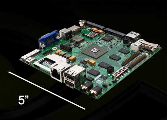
NVIDIA is supplying 5" development boards to its partners interested in Tegra 2. NVIDIA tells us that there are "hundreds" of these systems out in the wild. As you can guess by the size of the development board, the initial target for this chip isn't quite a smartphone.
The focus of today's announcement is unfortunately tablets. They are going to be able to make it to market quicker and are farther along the design process. While we don't expect any vendor to have completely nailed the perfect tablet yet, we should see some interesting UIs and form factors.
Multiple sources have now told me that the reason we never saw Tegra 1 in any smartphones or mainstream devices until the Zune HD was a simple case of NVIDIA arrogance. NVIDIA assumed that selling Tegra to phone manufacturers was just like selling GPUs to PC vendors, and it most definitely wasn't. It's been a long learning process, but NVIDIA appears to be better as a result.
There are Tegra 1 smartphones in flight right now. Presumably we'll see the first at this year's Mobile World Congress in Barcelona next month. There are also Tegra 2 smartphones that are currently being designed. We will see these before the end of 2010.
ARM Cortex A9: What I'm Excited About
NVIDIA won't talk about Tegra GPU architecture, but ARM is more than willing to talk about the Cortex A9.
I'm not used to seeing so much pipeline variance between microprocessor cores. The ARM11 core was introduced in 2003 and featured a single-issue 8-stage integer pipeline. Floating point was optional. The Cortex A8 was announced in 2005 and doubled the front end with. The A8 has a dual-issue in-order 13-stage integer pipeline. Doubling issue width increased IPC (instructions per clock) and the deeper pipeline gave it frequency headroom.
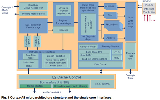
The Cortex A9 goes back down to an 8-stage pipeline. It's still a dual-issue pipeline, but instructions can execute out of order. What's even more ridiculous are the frequencies you can get out of this core. TI is going to be shipping a 750MHz and 1GHz SoC based on the Cortex A9. NVIDIA's Tegra 2 will run at up to 1GHz. And even ARM is willing to supply Cortex A9 designs that can run at up to 2GHz on TSMC's 40nm process. Privately I've heard that designs scaling beyond 2GHz, especially at 28nm, are going to be possible.
This is huge for two reasons. Cortex A9 has a shallower pipeline compared to A8, so it does more per clock. It also has an out of order execution engine, allowing it to also do more per clock. At the same clock speed, A9 should destroy A8. ARM estimates that the A8 can do up to 2 DMIPS per MHz (or 2000 DMIPS at 1GHz), whereas the A9 can do 2.5 DMIPS per MHz (2500 DMIPS at 1GHz). Given that most A8 implementations have been at or below 600MHz (1200 DMIPS), and TI's A9s are running at 750MHz or 1GHz (1875 DMIPS or 2500 DMIPS) I'd expect anywhere from a 30 - 100% performance improvement over existing Cortex A8 designs.
That's just for a single core though. At 40nm there's enough room to cram two of these out of order cores on a single SoC. That's what NVIDIA's doing at first with Tegra 2. Two cores together running multithreaded code and now you're looking at multiples of Cortex A8 performance. I'm talking iPhone to 3GS levels of performance improvement. And then some.
The shallower pipeline is very important for keeping power consumption low. Mispredicted branches have a much lower performance and power impact on shallow pipelines than they do on deep ones.
Each Cortex A9 MPCore has its own private L1 instruction and data caches. I'd expect these to be 32KB in size (each) just as they are today on the A8s. The L2 cache is shared by all cores on the SoC. A shared L2 makes sense, especially with a dual-core design. The architecture can scale up to 8MB of L2, but it seems a bit excessive. I'd expect L2 sizes to stay at around 256KB or 512KB. The L2 can run at the CPU's clock speed or for extremely high clocked versions of the A9 it can run at a divider.
What we're seeing is repetition of the sort of evolution we had in the desktop microprocessor, just on a much smaller scale. The Pentium processor was Intel's last high end in-order chip. The Pentium Pro brought out of order execution into the mix. ARM took that same evolutionary step going from the Cortex A8 to A9.
The world is very different today than it was when the Pentium Pro first came out. Multithreaded code is far more commonplace and thus we see that ARM's first out-of-order processor is also multi-core capable. Technically ARM11 could be used in multi-core environments, it just wasn't (at least not commonly). Even NVIDIA's Tegra 1 used the ARM11 MPCore processor, but only used one of them on its SoC. Cortex A9 will change all of that. The first implementations announced by TI as well as NVIDIA are dual-core designs. The next stage in smartphone evolution is enabling usable multitasking through interfaces like what we saw on the Palm Pre. In order to enable good performance in smartphone multitasking you'll need multiple cores.
There is of course a single core version of the Cortex A9. ARM suggests that the single core A9 is a great upgrade path for ARM11 designs. You get full backwards compatibility on code, an extremely small core (most ARM11 designs were 130nm, at 40nm a single A9 core is very space efficient) and much higher performance.
NEON Optional
With the Cortex A8 ARM introduced its own vector FP instruction set called NEON (think of it like ARM's SSE). A8 processors included a NEON core, but with Cortex A9 partners can either choose to use an ARM FPU or NEON. The FPU based Cortex A9s will most likely be single core implementations designed to be ARM11 replacements. The FPU will be smaller to implement than a full NEON unit and thus save cost/power.
Atom vs. Cortex A9
With Atom Intel adopted an in-order architecture to save power. With Cortex A9, ARM went out of order to improve performance. Despite the fundamental difference, Atom and ARM's Cortex A9 appear similar from a high level.
Atom has two instruction decoders at the front end, as does the A9. The dual decoders feed an instruction queue that can dispatch out of order:
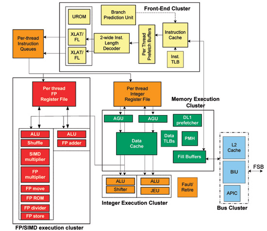
Intel's Atom Architecture
Both architectures appear to have a unified instruction queue that feed four dispatch ports. Atom has two ports that feed AGUs and/or ALUs, and two ports for the FPU (one for SSE and one for FP ops). A9 has two ALU ports, one FPU/NEON port and one AGU port.
Single-core ARM Cortex A9
Atom's advantage here is Hyper Threading as two threads get to share its execution resources simultaneously. Cortex A9's advantage is in a shallower pipeline and out of order execution. Both promote higher IPC but go about it in very different ways. If ARM can get clock speeds high enough they may actually have a higher performance option.
Final Words
Honestly, Tegra 2 is one of the most exciting things I've seen at CES - but it's mostly because of its dual Cortex A9 cores. While I'm excited about improving 3D graphics performance on tablets and smartphones, I believe general purpose performance needs improvement. ARM's Cortex A9 provides that improvement.
The days of me pestering smartphone vendors to drop ARM11 and embrace Cortex A8 are over. It's all about A9 now. NVIDIA delivers one solution with Tegra 2, but TI's OMAP 4 will also ship with a pair of A9s.
The big unknown continues to be actual, comparable power consumption. We're also lacking measurable graphics performance compared to the PowerVR SGX cores (particularly the SGX 540).
If NVIDIA is to be believed, then Tegra 2 is the SoC to get. I suspect that's being somewhat optimistic. But rest assured that if you're buying a smartphone in 2010, it's not Snapdragon that you want but something based on Cortex A9. NVIDIA is a viable option there and we'll have to wait until Mobile World Congress next month to see if there are any promising designs based on Tegra 2.
And just in case I wasn't clear earlier, we will see the first Tegra based Android phone in 2010. I just hope it's good.


