Original Link: https://www.anandtech.com/show/2849
NVIDIA's Fermi: Architected for Tesla, 3 Billion Transistors in 2010
by Anand Lal Shimpi on September 30, 2009 12:00 AM EST- Posted in
- GPUs
The graph below is one of transistor count, not die size. Inevitably, on the same manufacturing process, a significantly higher transistor count translates into a larger die size. But for the purposes of this article, all I need to show you is a representation of transistor count.
![]()
See that big circle on the right? That's Fermi. NVIDIA's next-generation architecture.
NVIDIA astonished us with GT200 tipping the scales at 1.4 billion transistors. Fermi is more than twice that at 3 billion. And literally, that's what Fermi is - more than twice a GT200.
At the high level the specs are simple. Fermi has a 384-bit GDDR5 memory interface and 512 cores. That's more than twice the processing power of GT200 but, just like RV870 (Cypress), it's not twice the memory bandwidth.
The architecture goes much further than that, but NVIDIA believes that AMD has shown its cards (literally) and is very confident that Fermi will be faster. The questions are at what price and when.
The price is a valid concern. Fermi is a 40nm GPU just like RV870 but it has a 40% higher transistor count. Both are built at TSMC, so you can expect that Fermi will cost NVIDIA more to make than ATI's Radeon HD 5870.
Then timing is just as valid, because while Fermi currently exists on paper, it's not a product yet. Fermi is late. Clock speeds, configurations and price points have yet to be finalized. NVIDIA just recently got working chips back and it's going to be at least two months before I see the first samples. Widespread availability won't be until at least Q1 2010.
I asked two people at NVIDIA why Fermi is late; NVIDIA's VP of Product Marketing, Ujesh Desai and NVIDIA's VP of GPU Engineering, Jonah Alben. Ujesh responded: because designing GPUs this big is "fucking hard".
Jonah elaborated, as I will attempt to do here today.
A Different Sort of Launch
Fermi will support DirectX 11 and NVIDIA believes it'll be faster than the Radeon HD 5870 in 3D games. With 3 billion transistors, it had better be. But that's the extent of what NVIDIA is willing to talk about with regards to Fermi as a gaming GPU. Sorry folks, today's launch is targeted entirely at Tesla.
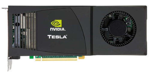
A GeForce GTX 280 with 4GB of memory is the foundation for the Tesla C1060 cards
Tesla is NVIDIA's High Performance Computing (HPC) business. NVIDIA takes its consumer GPUs, equips them with a ton of memory, and sells them in personal or datacenter supercomputers called Tesla supercomputers or computing clusters. If you have an application that can run well on a GPU, the upside is tremendous.
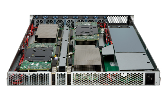
Four of those C1060 cards in a 1U chassis make the Tesla S1070. PCIe connects the S1070 to the host server.
NVIDIA loves to cite examples of where algorithms ported to GPUs work so much better than CPUs. One such example is a seismic processing application that HESS found ran very well on NVIDIA GPUs. It migrated a cluster of 2000 servers to 32 Tesla S1070s, bringing total costs down from $8M to $400K, and total power from 1200kW down to 45kW.
| HESS Seismic Processing Example | Tesla | CPU |
| Performance | 1 | 1 |
| # of Machines | 32 Tesla S1070s | 2000 x86 servers |
| Total Cost | ~$400K | ~$8M |
| Total Power | 45kW | 1200kW |
Obviously this doesn't include the servers needed to drive the Teslas, but presumably that's not a significant cost. Either way the potential is there, it's just a matter of how many similar applications exist in the world.
According to NVIDIA, there are many more cases like this in the market. The table below shows what NVIDIA believes is the total available market in the next 18 months for these various HPC segments:
| Processor | Seismic | Supercomputing | Universities | Defence | Finance |
| GPU TAM | $300M | $200M | $150M | $250M | $230M |
These figures were calculated by looking at the algorithms used in each segment, the number of Hess-like Tesla installations that can be done, and the current budget for non-GPU based computing in those markets. If NVIDIA met its goals here, the Tesla business could be bigger than the GeForce one. There's just one problem:
As you'll soon see, many of the architectural features of Fermi are targeted specifically for Tesla markets. The same could be said about GT200, albeit to a lesser degree. Yet Tesla accounted for less than 1.3% of NVIDIA's total revenue last quarter.
Given these numbers it looks like NVIDIA is building GPUs for a world that doesn't exist. NVIDIA doesn't agree.
The Evolution of GPU Computing
When matched with the right algorithms and programming efforts, GPU computing can provide some real speedups. Much of Fermi's architecture is designed to improve performance in these HPC and other GPU compute applications.
Ever since G80, NVIDIA has been on this path to bring GPU computing to reality. I rarely get the opportunity to get a non-marketing answer out of NVIDIA, but in talking to Jonah Alben (VP of GPU Engineering) I had an unusually frank discussion.
From the outside, G80 looks to be a GPU architected for compute. Internally, NVIDIA viewed it as an opportunistic way to enable more general purpose computing on its GPUs. The transition to a unified shader architecture gave NVIDIA the chance to, relatively easily, turn G80 into more than just a GPU. NVIDIA viewed GPU computing as a future strength for the company, so G80 led a dual life. Awesome graphics chip by day, the foundation for CUDA by night.
Remember that G80 was hashed out back in 2002 - 2003. NVIDIA had some ideas of where it wanted to take GPU computing, but it wasn't until G80 hit that customers started providing feedback that ultimately shaped the way GT200 and Fermi turned out.
One key example was support for double precision floating point. The feature wasn't added until GT200 and even then, it was only added based on computing customer feedback from G80. Fermi kicks double precision performance up another notch as it now executes FP64 ops at half of its FP32 rate (more on this later).
While G80 and GT200 were still primarily graphics chips, NVIDIA views Fermi as a processor that makes compute just as serious as graphics. NVIDIA believes it's on a different course, at least for the short term, than AMD. And you'll see this in many of the architectural features of Fermi.
Architecting Fermi: More Than 2x GT200
NVIDIA keeps referring to Fermi as a brand new architecture, while calling GT200 (and RV870) bigger versions of their predecessors with a few added features. Marginalizing the efforts required to build any multi-billion transistor chip is just silly, to an extent all of these GPUs have been significantly redesigned.
At a high level, Fermi doesn't look much different than a bigger GT200. NVIDIA is committed to its scalar architecture for the foreseeable future. In fact, its one op per clock per core philosophy comes from a basic desire to execute single threaded programs as quickly as possible. Remember, these are compute and graphics chips. NVIDIA sees no benefit in building a 16-wide or 5-wide core as the basis of its architectures, although we may see a bit more flexibility at the core level in the future.
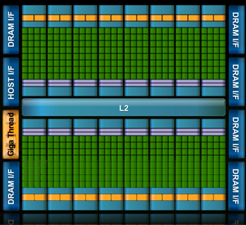
Despite the similarities, large parts of the architecture have evolved. The redesign happened at low as the core level. NVIDIA used to call these SPs (Streaming Processors), now they call them CUDA Cores, I’m going to call them cores.

All of the processing done at the core level is now to IEEE spec. That’s IEEE-754 2008 for floating point math (same as RV870/5870) and full 32-bit for integers. In the past 32-bit integer multiplies had to be emulated, the hardware could only do 24-bit integer muls. That silliness is now gone. Fused Multiply Add is also included. The goal was to avoid doing any cheesy tricks to implement math. Everything should be industry standards compliant and give you the results that you’d expect.
Double precision floating point (FP64) performance is improved tremendously. Peak 64-bit FP execution rate is now 1/2 of 32-bit FP, it used to be 1/8 (AMD's is 1/5). Wow.
NVIDIA isn’t disclosing clock speeds yet, so we don’t know exactly what that rate is yet.
In G80 and GT200 NVIDIA grouped eight cores into what it called an SM. With Fermi, you get 32 cores per SM.

The high end single-GPU Fermi configuration will have 16 SMs. That’s fewer SMs than GT200, but more cores. 512 to be exact. Fermi has more than twice the core count of the GeForce GTX 285.
| Fermi | GT200 | G80 | |
| Cores | 512 | 240 | 128 |
| Memory Interface | 384-bit GDDR5 | 512-bit GDDR3 | 384-bit GDDR3 |
In addition to the cores, each SM has a Special Function Unit (SFU) used for transcendental math and interpolation. In GT200 this SFU had two pipelines, in Fermi it has four. While NVIDIA increased general math horsepower by 4x per SM, SFU resources only doubled.
The infamous missing MUL has been pulled out of the SFU, we shouldn’t have to quote peak single and dual-issue arithmetic rates any longer for NVIDIA GPUs.
NVIDIA organizes these SMs into TPCs, but the exact hierarchy isn’t being disclosed today. With the launch's Tesla focus we also don't know specific on ROPs, texture filtering or anything else related to 3D graphics. Boo.
A Real Cache Hierarchy
Each SM in GT200 had 16KB of shared memory that could be used by all of the cores. This wasn’t a cache, but rather software managed memory. The application would have to knowingly move data in and out of it. The benefit here is predictability, you always know if something is in shared memory because you put it there. The downside is it doesn’t work so well if the application isn’t very predictable.
Branch heavy applications and many of the general purpose compute applications that NVIDIA is going after need a real cache. So with Fermi at 40nm, NVIDIA gave them a real cache.
Attached to each SM is 64KB of configurable memory. It can be partitioned as 16KB/48KB or 48KB/16KB; one partition is shared memory, the other partition is an L1 cache. The 16KB minimum partition means that applications written for GT200 that require 16KB of shared memory will still work just fine on Fermi. If your app prefers shared memory, it gets 3x the space in Fermi. If your application could really benefit from a cache, Fermi now delivers that as well. GT200 did have an L1 texture cache (one per TPC), but the cache was mostly useless when the GPU ran in compute mode.

The entire chip shares a 768KB L2 cache. The result is a reduced penalty for doing an atomic memory op, Fermi is 5 - 20x faster here than GT200.
A More Efficient Architecture
GPUs, like CPUs, work on streams of instructions called threads. While high end CPUs work on as many as 8 complicated threads at a time, GPUs handle many more threads in parallel.
The table below shows just how many threads each generation of NVIDIA GPU can have in flight at the same time:
| Fermi | GT200 | G80 | |
| Max Threads in Flight | 24576 | 30720 | 12288 |
Fermi can't actually support as many threads in parallel as GT200. NVIDIA found that the majority of compute cases were bound by shared memory size, not thread count in GT200. Thus thread count went down, and shared memory size went up in Fermi.
NVIDIA groups 32 threads into a unit called a warp (taken from the looming term warp, referring to a group of parallel threads). In GT200 and G80, half of a warp was issued to an SM every clock cycle. In other words, it takes two clocks to issue a full 32 threads to a single SM.
In previous architectures, the SM dispatch logic was closely coupled to the execution hardware. If you sent threads to the SFU, the entire SM couldn't issue new instructions until those instructions were done executing. If the only execution units in use were in your SFUs, the vast majority of your SM in GT200/G80 went unused. That's terrible for efficiency.
Fermi fixes this. There are two independent dispatch units at the front end of each SM in Fermi. These units are completely decoupled from the rest of the SM. Each dispatch unit can select and issue half of a warp every clock cycle. The threads can be from different warps in order to optimize the chance of finding independent operations.
There's a full crossbar between the dispatch units and the execution hardware in the SM. Each unit can dispatch threads to any group of units within the SM (with some limitations).
The inflexibility of NVIDIA's threading architecture is that every thread in the warp must be executing the same instruction at the same time. If they are, then you get full utilization of your resources. If they aren't, then some units go idle.
A single SM can execute:
| Fermi | FP32 | FP64 | INT | SFU | LD/ST |
| Ops per clock | 32 | 16 | 32 | 4 | 16 |
If you're executing FP64 instructions the entire SM can only run at 16 ops per clock. You can't dual issue FP64 and SFU operations.
The good news is that the SFU doesn't tie up the entire SM anymore. One dispatch unit can send 16 threads to the array of cores, while another can send 16 threads to the SFU. After two clocks, the dispatchers are free to send another pair of half-warps out again. As I mentioned before, in GT200/G80 the entire SM was tied up for a full 8 cycles after an SFU issue.
The flexibility is nice, or rather, the inflexibility of GT200/G80 was horrible for efficiency and Fermi fixes that.
Efficiency Gets Another Boon: Parallel Kernel Support
In GPU programming, a kernel is the function or small program running across the GPU hardware. Kernels are parallel in nature and perform the same task(s) on a very large dataset.
Typically, companies like NVIDIA don't disclose their hardware limitations until a developer bumps into one of them. In GT200/G80, the entire chip could only be working on one kernel at a time.
When dealing with graphics this isn't usually a problem. There are millions of pixels to render. The problem is wider than the machine. But as you start to do more general purpose computing, not all kernels are going to be wide enough to fill the entire machine. If a single kernel couldn't fill every SM with threads/instructions, then those SMs just went idle. That's bad.
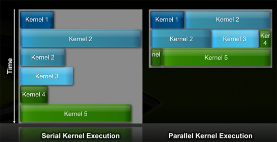
GT200 (left) vs. Fermi (right)
Fermi, once again, fixes this. Fermi's global dispatch logic can now issue multiple kernels in parallel to the entire system. At more than twice the size of GT200, the likelihood of idle SMs went up tremendously. NVIDIA needs to be able to dispatch multiple kernels in parallel to keep Fermi fed.
Application switch time (moving between GPU and CUDA mode) is also much faster on Fermi. NVIDIA says the transition is now 10x faster than GT200, and fast enough to be performed multiple times within a single frame. This is very important for implementing more elaborate GPU accelerated physics (or PhysX, great ;)…).
The connections to the outside world have also been improved. Fermi now supports parallel transfers to/from the CPU. Previously CPU->GPU and GPU->CPU transfers had to happen serially.
ECC Support
AMD's Radeon HD 5870 can detect errors on the memory bus, but it can't correct them. The register file, L1 cache, L2 cache and DRAM all have full ECC support in Fermi. This is one of those Tesla-specific features.
Many Tesla customers won't even talk to NVIDIA about moving their algorithms to GPUs unless NVIDIA can deliver ECC support. The scale of their installations is so large that ECC is absolutely necessary (or at least perceived to be).
Unified 64-bit Memory Addressing
In previous architectures there was a different load instruction depending on the type of memory: local (per thread), shared (per group of threads) or global (per kernel). This created issues with pointers and generally made a mess that programmers had to clean up.
Fermi unifies the address space so that there's only one instruction and the address of the memory is what determines where it's stored. The lowest bits are for local memory, the next set is for shared and then the remainder of the address space is global.
The unified address space is apparently necessary to enable C++ support for NVIDIA GPUs, which Fermi is designed to do.
The other big change to memory addressability is in the size of the address space. G80 and GT200 had a 32-bit address space, but next year NVIDIA expects to see Tesla boards with over 4GB of GDDR5 on board. Fermi now supports 64-bit addresses but the chip can physically address 40-bits of memory, or 1TB. That should be enough for now.
Both the unified address space and 64-bit addressing are almost exclusively for the compute space at this point. Consumer graphics cards won't need more than 4GB of memory for at least another couple of years. These changes were painful for NVIDIA to implement, and ultimately contributed to Fermi's delay, but necessary in NVIDIA's eyes.
New ISA Changes Enable DX11, OpenCL and C++, Visual Studio Support
Now this is cool. NVIDIA is announcing Nexus (no, not the thing from Star Trek Generations) a visual studio plugin that enables hardware debugging for CUDA code in visual studio. You can treat the GPU like a CPU, step into functions, look at the state of the GPU all in visual studio with Nexus. This is a huge step forward for CUDA developers.
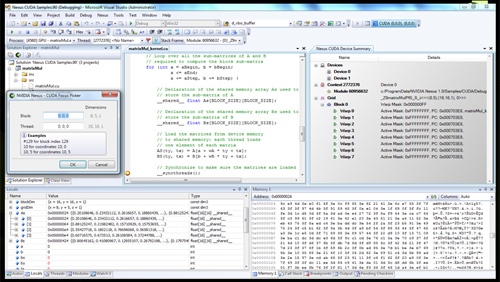
Nexus running in Visual Studio on a CUDA GPU
Simply enabling DX11 support is a big enough change for a GPU - AMD had to go through that with RV870. Fermi implements a wide set of changes to its ISA, primarily designed at enabling C++ support. Virtual functions, new/delete, try/catch are all parts of C++ and enabled on Fermi.
The RV770 Lesson (or The GT200 Story)
It took NVIDIA a while to give us an honest response to the RV770. At first it was all about CUDA and PhsyX. RV770 didn't have it, so we shouldn't be recommending it; that was NVIDIA's stance.
Today, it's much more humble.
Ujesh is wiling to take total blame for GT200. As manager of GeForce at the time, Ujesh admitted that he priced GT200 wrong. NVIDIA looked at RV670 (Radeon HD 3870) and extrapolated from that to predict what RV770's performance would be. Obviously, RV770 caught NVIDIA off guard and GT200 was priced much too high.
Ujesh doesn't believe NVIDIA will make the same mistake with Fermi.
Jonah, unwilling to let Ujesh take all of the blame, admitted that engineering was partially at fault as well. GT200 was the last chip NVIDIA ever built at 65nm - there's no excuse for that. The chip needed to be at 55nm from the get-go, but NVIDIA had been extremely conservative about moving to new manufacturing processes too early.
It all dates back to NV30, the GeForce FX. It was a brand new architecture on a bleeding edge manufacturing process, 130nm at the time, which ultimately lead to its delay. ATI pulled ahead with the 150nm Radeon 9700 Pro and NVIDIA vowed never to make that mistake again.
With NV30, NVIDIA was too eager to move to new processes. Jonah believes that GT200 was an example of NVIDIA swinging too far in the other direction; NVIDIA was too conservative.
The biggest lesson RV770 taught NVIDIA was to be quicker to migrate to new manufacturing processes. Not NV30 quick, but definitely not as slow as GT200. Internal policies are now in place to ensure this.
Architecturally, there aren't huge lessons to be learned from RV770. It was a good chip in NVIDIA's eyes, but NVIDIA isn't adjusting their architecture in response to it. NVIDIA will continue to build beefy GPUs and AMD appears committed to building more affordable ones. Both companies are focused on building more efficiently.
Of Die Sizes and Transitions
Fermi and Cypress are both built on the same 40nm TSMC process, yet they differ by nearly 1 billion transistors. Even the first generation Larrabee will be closer in size to Cypress than Fermi, and it's made at Intel's state of the art 45nm facilities.
What you're seeing is a significant divergence between the graphics companies, one that I expect will continue to grow in the near term.
NVIDIA's architecture is designed to address its primary deficiency: the company's lack of a general purpose microprocessor. As such, Fermi's enhancements over GT200 address that issue. While Fermi will play games, and NVIDIA claims it will do so better than the Radeon HD 5870, it is designed to be a general purpose compute machine.
ATI's approach is much more cautious. While Cypress can run DirectX Compute and OpenCL applications (the former faster than any NVIDIA GPU on the market today), ATI's use of transistors was specifically targeted to run the GPU's killer app today: 3D games.
Intel's take is the most unique. Both ATI and NVIDIA have to support their existing businesses, so they can't simply introduce a revolutionary product that sacrifices performance on existing applications for some lofty, longer term goal. Intel however has no discrete GPU business today, so it can.
Larrabee is in rough shape right now. The chip is buggy, the first time we met it it wasn't healthy enough to even run a 3D game. Intel has 6 - 9 months to get it ready for launch. By then, the Radeon HD 5870 will be priced between $299 - $349, and Larrabee will most likely slot in $100 - $150 cheaper. Fermi is going to be aiming for the top of the price brackets.
The motivation behind AMD's "sweet spot" strategy wasn't just die size, it was price. AMD believed that by building large, $600+ GPUs, it didn't service the needs of the majority of its customers quickly enough. It took far too long to make a $199 GPU from a $600 one - quickly approaching a year.
Clearly Fermi is going to be huge. NVIDIA isn't disclosing die sizes, but if we estimate that a 40% higher transistor count results in a 40% larger die area then we're looking at over 467mm^2 for Fermi. That's smaller than GT200 and about the size of G80; it's still big.
I asked Jonah if that meant Fermi would take a while to move down to more mainstream pricepoints. Ujesh stepped in and said that he thought I'd be pleasantly surprised once NVIDIA is ready to announce Fermi configurations and price points. If you were NVIDIA, would you say anything else?
Jonah did step in to clarify. He believes that AMD's strategy simply boils down to targeting a different price point. He believes that the correct answer isn't to target a lower price point first, but rather build big chips efficiently. And build them so that you can scale to different sizes/configurations without having to redo a bunch of stuff. Putting on his marketing hat for a bit, Jonah said that NVIDIA is actively making investments in that direction. Perhaps Fermi will be different and it'll scale down to $199 and $299 price points with little effort? It seems doubtful, but we'll find out next year.
Final Words
Today's launch is strange. I tried to convince NVIDIA to release more information about Fermi but was met with staunch resistance from the company. NVIDIA claims that by pre-announcing Fermi's performance levels it would seriously hurt its existing business. It's up to you whether or not you want to believe that.
Last quarter the Tesla business unit made $10M. That's not a whole lot of money for a company that, at its peak, grossed $1B in a single quarter. NVIDIA believes that Fermi is when that will all change. To borrow a horrendously overused phrase, Fermi is the inflection point for NVIDIA's Tesla sales.
By adding support for ECC, enabling C++ and easier Visual Studio integration, NVIDIA believes that Fermi will open its Tesla business up to a group of clients that would previously not so much as speak to NVIDIA. ECC is the killer feature there.
While the bulk of NVIDIA's revenue today comes from 3D graphics, NVIDIA believes that Tegra (mobile) and Tesla are the future growth segments for the company. This hints at a very troubling future for GPU makers - are we soon approaching the Atom-ization of graphics cards?
Will 2010 be the beginning of good enough performance in PC games? Display resolutions have pretty much stagnated, PC games are first developed on consoles which have inferior hardware and thus don't have as high the GPU requirements. The fact that NVIDIA is looking to Tegra and Tesla to grow the company is very telling. Then again, perhaps a brand new approach to graphics is what we'll need for the re-invigoration of PC game development. Larrabee.
If the TAM for GPUs in HPC is so big, why did NVIDIA only make $10M last quarter? If you ask NVIDIA it has to do with focus and sales.
According to NVIDIA, over the past couple of years NVIDIA's Tesla sales efforts have been scattered. The focus was on selling to any customers that could potentially see a speedup, trying to gain some traction for the Tesla business.
Jen-Hsun did some yelling and now NVIDIA is a bit more focused in that department. If Tesla revenues increase linearly from this point, that's simply not going to be enough. I asked NVIDIA if exponential growth for Tesla was in the cards and if so, when would it happen. The answer was yes and with Fermi.
We'll see how that plays out, but if Fermi doesn't significantly increase Tesla revenues then we know that NVIDIA is in serious trouble.
The architecture looks good, Fermi just needs to be priced right. Oh and the chip needs to hurry up and come out.


