Original Link: https://www.anandtech.com/show/2556
The Radeon HD 4850 & 4870: AMD Wins at $199 and $299
by Anand Lal Shimpi & Derek Wilson on June 25, 2008 12:00 AM EST- Posted in
- GPUs
...and then disaster struck.
Or at least that's how it felt. The past few weeks have been incredibly tumultuous, sleepless, and beyond interesting. It is as if AMD and NVIDIA just started pulling out hardware and throwing it at eachother while we stood in the middle getting pegged with graphics cards. And we weren't just hit with new architectures and unexpected die shrinks, but new drivers left and right.
First up was GT200, which appeared in the form of the GeForce GTX 280 and GeForce GTX 260. Of course, both of those can be paired or tri-ed (if you will), but with two cards requiring at least a 1200W PSU we're a bit worried of trying three. Then came the randomness that was the accidental launch of the Radeon HD 4850 (albeit with no architectural information) and only a couple hours later we first heard about the 9800 GTX+ which is a die shrunk higher clocked 9800 GTX that is now publicly announced and will be available in July.
And now we have the other thing we've been working on since we finished GT200: RV770 in all it's glory. This includes the 4850 whose performance we have already seen and the Radeon HD 4870: the teraflop card that falls further short of hitting its theoretical performance than NVIDIA did with GT200. But theoretical performance isn't reality, and nothing can be done if every instruction is a multiply-add or combination of a multiply-add and a multiply, so while marketing loves to trot out big numbers we quite prefer real-world testing with games people will actually play on this hardware.
But before we get to performance, and as usual, we will want to take as deep a look into this architecture as possible. We won't be able to go as deep with RV770 as we could with GT200, as we had access to a lot of information both from NVIDIA and from outside NVIDIA that allowed us to learn more about their architecture. At the same time, we still know barely anything about the real design of either NVIDIA or AMD's hardware as they prefer to hold their cards very close.
This won't work long term, however. As we push toward moving compute intensive applications to the GPU, developers will not just want -- they will need low level architectural information. It is impossible to properly optimize code for an architecture when you don't know exact details about timing, latency, cache sizes, register files, resource sharing, and the like. While, this generation, we have decidedly more information from NVIDIA on how to properly program their architecture, we still need more from both AMD and NVIDIA.
And Now, the Rest of the Story
Last week was a weird teaser - we gave you the goods, without explaining what they were.


By now you know that the Radeon HD 4850 is the best buy at $199, but today we're able to tell you much about its inner workings as well as introduce its faster, more expensive sibling: the Radeon HD 4870.
| ATI Radeon HD 4870 | ATI Radeon HD 4850 | ATI Radeon HD 3870 | |
| Stream Processors | 800 | 800 | 320 |
| Texture Units | 40 | 40 | 16 |
| ROPs | 16 | 16 | 16 |
| Core Clock | 750MHz | 625MHz | 775MHz+ |
| Memory Clock | 900MHz (3600MHz data rate) GDDR5 | 993MHz (1986MHz data rate) GDDR3 | 1125MHz (2250MHz data rate) GDDR4 |
| Memory Bus Width | 256-bit | 256-bit | 256-bit |
| Frame Buffer | 512MB | 512MB | 512MB |
| Transistor Count | 956M | 956M | 666M |
| Manufacturing Process | TSMC 55nm | TSMC 55nm | TSMC 55nm |
| Price Point | $299 | $199 | $199 |
Priced at $299 the Radeon HD 4870 is clocked 20% higher and has 81% more memory bandwidth than the Radeon HD 4850. The GPU clock speed improvement is simply due to better cooling as the 4870 ships with a two-slot cooler. The memory bandwidth improvement is due to the Radeon HD 4870 using GDDR5 memory instead of GDDR3 used on the 4850 (and GDDR4 for 3870); the result is a data rate equal to 4x the memory clock speed or 3.6Gbps. The Radeon HD 4870 and 4850 both use a 256-bit memory bus like the 3870 before it (as well as NVIDIA's competing GeForce 9800 GTX), but total memory bandwidth on the 4870 ends up being 115.2GB/s thanks to the use of GDDR5. Note that this is more memory bandwidth than the GeForce GTX 260 which has a much wider 448-bit memory bus, but uses GDDR3 devices.
| NVIDIA GeForce GTX 280 | NVIDIA GeForce GTX 260 | NVIDIA GeForce 9800 GTX | ATI Radeon HD 4870 | ATI Radeon HD 4850 | ATI Radeon HD 3870 | |
| Memory Size | 1GB | 896MB | 512MB | 512MB | 512MB | 512MB |
| Memory Technology | GDDR3 | GDDR3 | GDDR3 | GDDR5 | GDDR3 | GDDR4 |
| Memory Bus Width | 512-bit | 448-bit | 256-bit | 256-bit | 256-bit | 256-bit |
| Memory Clock | 1107MHz | 999MHz | 1100MHz | 900MHz | 993MHz | 1125MHz |
| Memory Data Rate | 2.2Gbps | 2.0Gbps | 2.22Gbps | 3.6Gbps | 1.99Gbps | 2.25Gbps |
| Memory Bandwidth | 141.7GB/s | 111.9GB/s | 70.4GB/s | 115.2GB/s | 63.6GB/s | 72.0GB/s |
The use of GDDR5 enabled AMD to deliver GeForce GTX 260 class memory bandwidth, but without the pin-count and expense of a 448-bit memory interface. GDDR5 actually implements a number of Rambus-like routing and signaling technologies while still remaining a parallel based memory technology, the result is something that appears to deliver tremendous bandwidth per pin in a reliable, high volume solution.
AMD most likely took a risk on bringing GDDR5 to market this early and we do expect NVIDIA to follow suit, AMD is simply enjoying the benefits of jumping on the GDDR5 bandwagon early and getting it right, at least it seems that way. It wouldn't be too far fetched to imagine a 55nm GT200 die shrink with a 256-bit GDDR5 memory interface, it should allow NVIDIA to drop the price down to the $300 level (at least for the GTX 260).
As we mentioned in our Radeon HD 4850 Preview, both the Radeon HD 4870 and 4850 now support 8-channel LPCM audio output over HDMI. AMD just sent over 8-channel LPCM drivers for the Radeon HD 4870 so we'll be testing this functionality shortly. As we mentioned in our 4850 preview:
"All of AMD's Radeon HD graphics cards have shipped with their own audio codec, but the Radeon HD 4800 series of cards finally adds support for 8-channel LPCM output over HDMI. This is a huge deal for HTPC enthusiasts because now you can output 8-channel audio over HDMI in a motherboard agnostic solution. We still don't have support for bitstreaming TrueHD/DTS-HD MA and most likely won't anytime this year from a GPU alone, but there are some other solutions in the works for 2008."
The Radeon HD 4870 is scheduled for widespread availability in early July, although AMD tells us that some cards are already in the channel. Given that the 4870 relies on a new memory technology, we aren't sure how confident we can be that it will be as widely available as the Radeon HD 4850 has been thus far. Keep an eye out but so far the 4850 has been shipping without any issues at $199 or below, so as long as AMD can get cards in retailers' hands we expect the 4870 to hit its $299 price point.
AMD's "Small-Die" Strategy
We outlined AMD's "new" GPU strategy in our Radeon HD 4850 preview article, but in short AMD has committed to designing GPUs for the mainstream $199 - $299 segment and simply using CrossFire (multi-GPU) to address higher end markets. NVIDIA on the other hand will continue to make very large monolithic GPUs in order to continue to push the industry forward. Both approaches are appreciated and necessary, they simply target different markets.
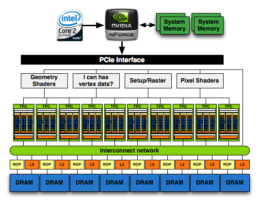
In our GT200 review we highlighted the fact that NVIDIA had built an extremely large, highly parallel, microprocessor. With 1.4 billion transistors and a die size of around 576 mm^2, NVIDIA's GT200 is nothing short of huge.
The table on the previous page shows that AMD's RV770, despite being aimed at mainstream gamer price points ($199 - $299), is also very large. At 956M transistors, the RV770 has 44% more transistors than RV670 and 68% the transistor count of NVIDIA's GT200. We threw the RV770 into NVIDIA's die size comparison just for kicks:
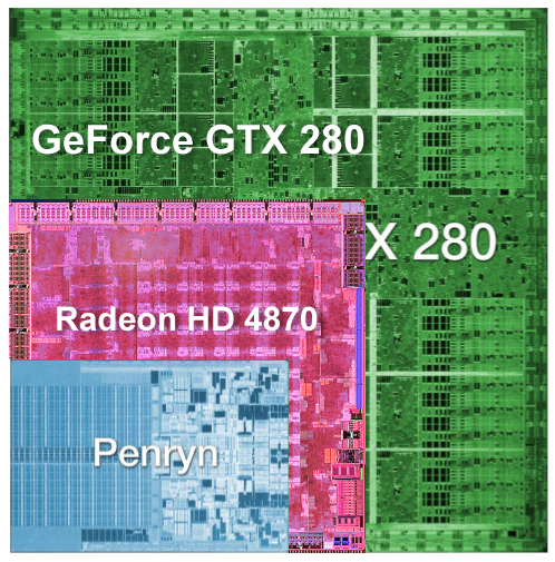
Based on what we know of NVIDIA's die size, this should be to scale
Even AMD's die, although designed to be svelte and affordable, is big - especially for being fabbed at TSMC. NVIDIA still holds the crown for largest die fabbed at TSMC, but AMD shows us that even a more mainstream approach still requires tons of transistors. As we mentioned in our 4850 preview:
"A pair of RV770s, AMD's new GPU, end up consuming more power than a single GT200 - despite being built on a smaller 55nm process.
A pair of these RV770s only costs $400 compared to $650 for a single GT200, but I suspect that part of that is due to differences in manufacturing process. If NVIDIA hadn't been so risk averse with the GT200 and built it on 55nm (not that I'm advocating it, simply posing a hypothetical), the cost differences would be smaller - if not in favor of NVIDIA since GT200 is built on a single card.
When the smoke clears, AMD's strategy is to simply build a GPU for the masses and attempt to scale it up and down. While NVIDIA is still building its GPUs the same way it has for decades, starting very large and scaling down.
AMD isn't taking a radically different approach to building and designing GPUs than NVIDIA, it's simply building one market segment lower."
We've got a lot of discussion on efficiency between AMD and NVIDIA coming up in this article, although AMD's die is noticeably smaller than NVIDIA's - as you've already seen with the Radeon HD 4850 - there are many areas where RV770 can go toe-to-toe with NVIDIA's mammoth GT200.
Building a RV770
We did this with NVIDIA's GT200 and it seemed to work out well, so let's start at the most basic level with AMD's RV770. Meet the Stream Processing Unit:
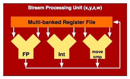
AMD's Stream Processing Unit is very similar to NVIDIA's SP in G80/G92/GT200, so similar in fact that I drew them the same way. Keep in mind that the actual inner workings of one of these units is far more complex than three ALUs but to keep things simple and consistent that's how I drew it (the actual hardware is a fused FP MUL + ADD unit, for those who care). AMD has four of these stream processing units in a processor block and they are called x, y, z or w units.
There's a fifth unit called a t-unit (the t stands for transcendental, meaning the type of operations it is capable of processing):
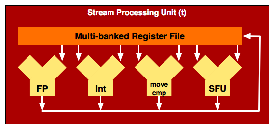
The t-unit can do everything a x,y,z or w-unit can do, but it also can do transcendental operations (represented by the SFU block in the diagram above). NVIDIA has the same functionality, it simply chooses to expose it in a different way (which we'll get to shortly). AMD considers each one of these units (x,y,z,w and t) a processing unit, and the RV770 has 800 of them (the RV670 had 320).
AMD pairs four of these stream processing units (x,y,z and w) with a t-unit and puts them together as a block, which I have decided to call a Streaming Processor (SP):
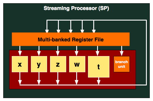
The area in red is actually the SP, but unlike one of NVIDIA's SPs, one of AMD's can handle up to five instructions at the same time. The only restriction here is that all five units have to be working on the same thread.
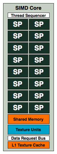
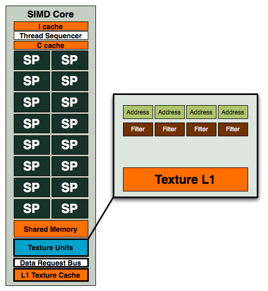
AMD then groups 16 of these SPs into something they like to call a SIMD core (AMD has less confusing, but far worse names for its architectural elements than NVIDIA):
|
AMD's SIMD Core
|
NVIDIA's SM
|
 |
 |
A SIMD core is very similar to NVIDIA's SM with a couple of exceptions:
1) There are more SPs in AMD's SIMD Core (16 vs 8)
2) The SPs are wider and can process, at peak, 5x the number of instructions as NVIDIA's SPs
3) The Instruction and Constant caches are not included in the SIMD core, AMD places them further up the ladder.
4) AMD pairs its texture units and texture cache with its SPs at the SIMD core level, while NVIDIA does it further up the ladder.
5) See the two SFUs in NVIDIA's SM? While NVIDIA has two very fast Special Function Units in its SM, AMD equips each SP with its own SFU. It's unclear which approach is actually faster given that we don't know the instruction latency or throughput of either SFU.
Note that at this point, the RV770 is really no different than the RV670 (the GPU used in the Radeon HD 3870). The next step is where AMD and NVIDIA really diverge; while NVIDIA's GT200 takes three SMs and groups them into a Texture/Processing Cluster (TPC) and then arranging 10 TPCs on its chip, AMD simply combines 10 SIMD cores:
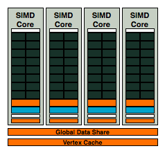
AMD's RV670
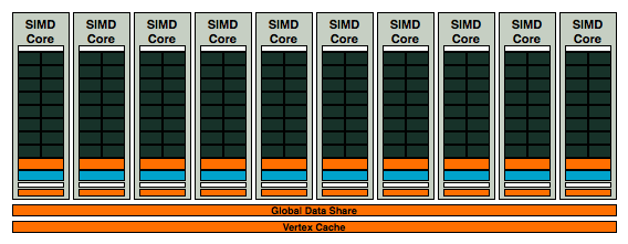
10 SIMD cores at your disposal in AMD's RV770, this is how AMD goes from competitive, to downright threatening
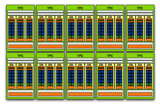
NVIDIA's GT200 Streaming Processor Array (SPA), it has fewer execution resources but more encapsulation around them, the focus here is on thread management
With 10 SIMD cores the RV770, it has 2.5x the number of execution units as a RV670. It even has more theoretical processing power than NVIDIA's GT200. If you just look at the number of concurrent instructions that can be processed on RV770 vs. GT200, the RV770's 800 execution units to GT200's 240 (+ 60 SFUs) is in a completely different league.
| NVIDIA GT200 | AMD RV770 | AMD RV670 | |
| SP Issue Width | 1-way | 5-way | 5-way |
| # of SPs | 240 | 160 | 64 |
| Worst Case Dependent Instruction Throughput | 240 | 160 | 64 |
| Maximum Scalar Instruction Throughput | 480* | 800 | 320 |
We'll be talking about efficiency and resource utilization in the coming pages, but immediately you'll notice that the RV770 (like the RV670 and R600 that came before it) has the potential to be slower than NVIDIA's architectures or significantly faster, depending entirely on how instruction or thread heavy the workload is. NVIDIA's architecture prefers tons of simple threads (one thread per SP) while AMD's architecture wants instruction heavy threads (since it can work on five instructions from a single thread at once).
NVIDIA's GeForce GTX 280
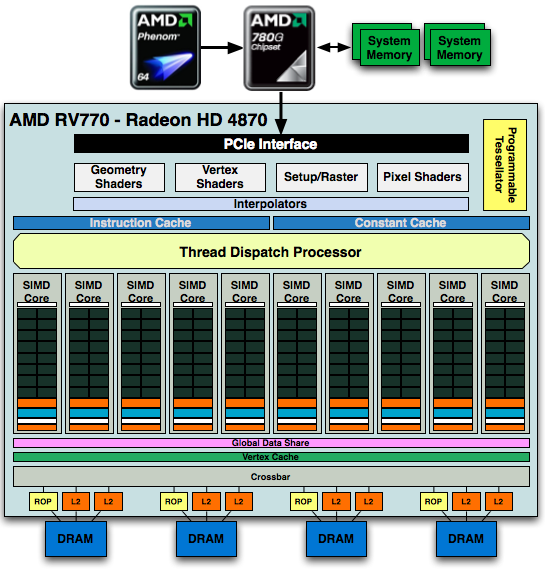
AMD's Radeon HD 4870
The full GPU is pretty impressive:
1) See the Instruction and Constant Caches up top? NVIDIA includes them in each SM while AMD seems to include them outside of the SIMD core clusters.
2) The RV770 only has four 64-bit memory controllers compared to the eight in GT200
3) The Programmable Tessellator is left over from the Xbox 360's GPU (and R600/RV670), unfortunately it is unused by most developers as there is no DirectX support for it yet.
4) AMD has dedicated hardware attribute interpolators, something NVIDIA's hardware shares with its special function units (SFUs).
Other than the differences we mentioned above, AMD's architecture is similar in vain to NVIDIA's, there are just a handful of design choices that set the two apart. Just like NVIDIA took its G80/G92 architecture and made it larger, AMD did the same with RV770 - it took RV670 and more than doubled its execution resources.
AMD took a bigger leap with RV770 from RV670 than NVIDIA did from G80/G92 to GT200, but it makes sense given that AMD had to be more competitive than it even was in the last generation.
That Darn Compute:Texture Ratio
With its GT200 GPU, NVIDIA increased compute resources by nearly 90% but only increased texture processing by 25%, highlighting a continued trend in making GPUs even more powerful computationally. Here's another glance at the GT200's texture address and filter units:
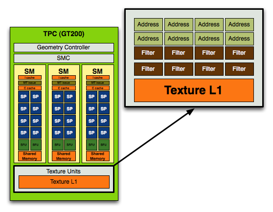
Each TPC, of which there are 10, has eight address and eight filter units. Now let's look at RV770:
Four address and four filter units, while AMD maintains the same 1:1 address-to-filter ratio that NVIDIA does, the ratio of compute-to-texture in RV770 is significantly higher.
| AMD RV770 | AMD RV670 | NVIDIA GT200 | NVIDIA G92 | |
| # of SPs | 160 | 64 | 240 | 128 |
| Texture Address/Filter Units | 40 / 40 | 16 / 16 | 80 / 80 | 64 / 64 |
| Compute to Texture Ratio | 4:1 | 4:1 | 3:1 | 2:1 |
The table above illustrates NVIDIA's trend of increasing the compute to texture ratio from 2:1 in G92 to 3:1 in GT200. AMD arguably overshot with RV670 and its 4:1 ratio and thus didn't need to adjust it with RV770. Even while staying still at 4:1 with RV770, AMD's ratio is still more aggressively geared towards compute than NVIDIA's is. That does mean that more texture bound games will do better on NVIDIA hardware (at least proportionally), while more compute intensive games may do better on RV770.
AMD did also make some enhancements to their texture units as well. By doing some "stuff" that they won't tell us about, they improved the performance per mm^2 by 70%. Texture cache bandwidth has also been doubled to 480 GB/s while bandwidth between each L1 cache and L2 memory is 384 GB/s. L2 caches are aligned with memory channels of which there are four interleaved channels (resulting in 8 L2 caches).
Now that texture units are linked to both specific SIMD cores and individual L1 texture caches, we have an increase in total texturing ability due to the increase in SIMD cores with RV770. This gives us a 2.5x increase in the number of 8-bit per component textures we can fetch and bilinearly filter per clock, but only a 1.25x increase in the number of fp16 textures (as fp16 runs at half rate and fp32 runs at one quarter rate). It was our understanding that fp16 textures could run at full speed on R600, so the 1.25x increase in performance for half rate texturing of fp16 data makes sense.
Even though fp32 runs at quarter rate, with the types of texture fetches we would need to do, AMD says that we could end up being external memory bandwidth bound before we are texture filtering hardware bound. If this is the case, then the design decision to decrease rates for higher bit-depth textures makes sense.
| AMD RV770 | AMD RV670 | |
| L1 Texture Cache | 10 x 16KB (160KB total) | 32KB |
| L2 Texture Cache | I can has cache size? | 256KB |
| Vertex Cache | ? | 32KB |
| Local Data Share | 16KB | None |
| Global Data Share | 16KB | ? |
Even though AMD wouldn't tell us L1 cache sizes, we had enough info left over from the R600 time frame to combine with some hints and extract the data. We have determined that RV770 has 10 distinct 16k caches. This is as opposed to the single shared 32k L1 cache on R600 and gives us a total of 160k of L1 cache. We know R600's L2 cache was 256k, and AMD told us RV770 has a larger L2 cache, but they wouldn't give us any hints to help out.
Derek Gets Technical Again: Of Warps, Wavefronts and SPMD
From our GT200 review, we learned a little about thread organization and scheduling on NVIDIA hardware. In speaking with AMD we discovered that sometimes it just makes sense to approach the solution to a problem in similar ways. Like NVIDIA, AMD schedules threads in groups (called wavefronts by AMD) that execute over 4 cycles. As RV770 has 16 5-wide SPs (each of which process one "stream" or thread or whatever you want to call it) at a time (and because they said so), we can conclude that AMD organizes 64 threads into one wavefront which all must execute in parallel. After GT200, we did learn that NVIDIA further groups warps into thread blocks, and we just learned that their are two more levels of organization in AMD hardware.
Like NVIDIA, AMD maintains context per wavefront: register space, instruction stream, global constants, and local store space are shared between all threads running in a wavefront and data sharing and synchronization can be done within a thread block. The larger grouping of thread blocks enables global data sharing using the global data store, but we didn't actually get a name or specification for it. On RV770 one VLIW instruction (up to 5 operations) is broadcast to each of the SPs which runs on it's own unique set of data and subset of the register file.
To put it side by side with NVIDIA's architecture, we've put together a table with what we know about resources per SM / SIMD array.
| NVIDIA/AMD Feature | NVIDIA GT200 | AMD RV770 |
| Registers per SM/SIMD Core | 16K x 32-bit | 16K x 128-bit |
| Registers on Chip | 491,520 (1.875MB) | 163,840 (2.5MB) |
| Local Store | 16KB | 16KB |
| Global Store | None | 16KB |
| Max Threads on Chip | 30,720 | 16,384 |
| Max Threads per SM/SIMD Core | 1,024 | > 1,000 |
| Max Threads per Warp/Wavefront | 960 | 256 (with 64 reserved) |
| Max Warps/Wavefronts on Chip | 512 | We Have No Idea |
| Max Thread Blocks per SM/SIMD Core | 8 | AMD Won't Tell Us |
We love that we have all this data, and both NVIDIA's CUDA programming guide and the documentation that comes with AMD's CAL SDK offer some great low level info. But the problem is that hard core tuners of code really need more information to properly tune their applications. To some extent, graphics takes care of itself, as there are a lot of different things that need to happen in different ways. It's the GPGPU crowd, the pioneers of GPU computing, that will need much more low level data on how resource allocation impacts thread issue rates and how to properly fetch and prefetch data to make the best use of external and internal memory bandwidth.
But for now, these details are the ones we have, and we hope that programmers used to programming massively data parallel code will be able to get under the hood and do something with these architectures even before we have an industry standard way to take advantage of heterogeneous computing on the desktop.
Which brings us to an interesting point.
NVIDIA wanted us to push some ridiculous acronym for their SM's architecture: SIMT (single instruction multiple thread). First off, this is a confusing descriptor based on the normal understanding of instructions and threads. But more to the point, there already exists a programming model that nicely fits what NVIDIA and AMD are both actually doing in hardware: SPMD, or single program multiple data. This description is most often attached to distributed memory systems and large scale clusters, but it really is actually what is going on here.
Modern graphics architectures process multiple data sets (such as a vertex or a pixel and its attributes) with single programs (a shader program in graphics or a kernel if we're talking GPU computing) that are run both independently on multiple "cores" and in groups within a "core". Functionally we maintain one instruction stream (program) per context and apply it to multiple data sets, layered with the fact that multiple contexts can be running the same program independently. As with distributed SPMD systems, not all copies of the program are running at the same time: multiple warps or wavefronts may be at different stages of execution within the same program and support barrier synchronization.
For more information on the SPMD programming model, wikipedia has a good page on the subject even though it doesn't talk about how GPUs would fit into SPMD quite yet.
GPUs take advantage of a property of SPMD that distributed systems do not (explicitly anyway): fine grained resource sharing with SIMD processing where data comes from multiple threads. Threads running the same code can actually physically share the same instruction and data caches and can have high speed access to each others data through a local store. This is in contrast to larger systems where each system gets a copy of everything to handle in its own way with its own data at its own pace (and in which messaging and communication become more asynchronous, critical and complex).
AMD offers an advantage in the SPMD paradigm in that it maintains a global store (present since RV670) where all threads can share result data globally if they need to (this is something that NVIDIA does not support). This feature allows more flexibility in algorithm implementation and can offer performance benefits in some applications.
In short, the reality of GPGPU computing has been the implementation in hardware of the ideal machine to handle the SPMD programming model. Bits and pieces are borrowed from SIMD, SMT, TMT, and other micro-architectural features to build architectures that we submit should be classified as SPMD hardware in honor of the programming model they natively support. We've already got enough acronyms in the computing world, and it's high time we consolidate where it makes sense and stop making up new terms for the same things.
A Quick Primer on ILP
NVIDIA throws ILP (instruction level parallelism) out the window while AMD tackles it head on.
ILP is parallelism that can be extracted from a single instruction stream. For instance, if i have a lot of math that isn't dependent on previous instructions, it is perfectly reasonable to execute all this math in parallel.
For this example on my imaginary architecture, instruction format is:
LineNumber INSTRUCTION dest-reg, source-reg-1, source-reg-2


This is compiled code for adding 8 numbers together. (i.e. A = B + C + D + E + F + G + H + I;)


1 ADD r2,r0,r1

2 ADD r5,r3,r4

3 ADD r8,r6,r7

4 ADD r11,r9,r10

5 ADD r12,r2,r5

6 ADD r13,r8,r11

7 ADD r14,r12,r13

8 [some totally independent instruction]

...
Lines 1,2,3 and 4 could all be executed in parallel if hardware is available to handle it. Line 5 must wait for lines 1 and 2, line 6 must wait for lines 3 and 4, and line 7 can't execute until all other computation is finished. Line 8 can execute at any point hardware is available.
For the above example, in two wide hardware we can get optimal throughput (and we ignore or assume full speed handling of read-after-write hazards, but that's a whole other issue). If we are looking at AMD's 5 wide hardware, we can't achieve optimal throughput unless the following code offers much more opportunity to extract ILP. Here's why:
From the above block, we can immediately execute 5 operations at once: lines 1,2,3,4 and 8. Next, we can only execute two operations together: lines 5 and 6 (three execution units go unused). Finally, we must execute instruction 7 all by itself leaving 4 execution units unused.
The limitations of extracting ILP are on the program itself (the mix of independent and dependent instructions), the hardware resources (how much can you do at once from the same instruction stream), the compiler (how well does the compiler organize basic blocks into something the hardware can best extract ILP from) and the scheduler (the hardware that takes independent instructions and schedules them to run simultaneously).
Extracting ILP is one of the most heavily researched areas of computing and was the primary focuses of CPU design until the advent of multicore hardware. But it is still an incredibly tough problem to solve and the benefits vary based on the program being executed.
The instruction stream above is sent to an AMD and NVIDIA SP. In the best case scenario, the instruction stream going into AMD's SP should be 1/5th the length of the one going into NVIDIA's SP (as in, AMD should be executing 5 ops per SP vs. 1 per SP for NVIDIA) but as you can see in this exampe, the instruction stream is around half the height of the one in the NVIDIA column. The more ILP AMD can extract from the instruction stream, the better its hardware will do.
AMD's RV770 (And R6xx based hardware) needs to schedule 5 operations per thread every every clock to get the most out of their hardware. This certainly requires a bit of fancy compiler work and internal hardware scheduling, which NVIDIA doesn't need to bother with. We'll explain why in a second.
Instruction Issue Limitations and ILP vs TLP Extraction
Since a great deal of graphics code manipulates vectors like vertex positions (x,y,c,w) or colors (r,g,b,a), lots of things happen in parallel anyway. This is a fine and logical aspect of graphics to exploit, but when it comes down to it the point of extracting parallelism is simply to maximize utilization of hardware (after all, everything in a scene needs to be rendered before it can be drawn) and hide latency. Of course, building a GPU is not all about extracting parallelism, as AMD and NVIDIA both need to worry about things like performance per square millimeter, performance per watt, and suitability to the code that will be running on it.
NVIDIA relies entirely on TLP (thread level parallelism) while AMD exploits both TLP and ILP. Extracting TLP is much much easier than ILP, as the only time you need to worry about any inter-thread conflicts is when sharing data (which happens much less frequently than does dependent code within a single thread). In a graphics architecture, with the necessity of running millions of threads per frame, there are plenty of threads with which to fill the execution units of the hardware, and thus exploiting TLP to fill the width of the hardware is all NVIDIA needs to do to get good utilization.
There are ways in which AMD's architecture offers benefits though. Because AMD doesn't have to context switch wavefronts every chance it gets and is able to extract ILP, it can be less sensitive to the number of active threads running than NVIDIA hardware (however both do require a very large number of threads to be active to hide latency). For NVIDIA we know that to properly hide latency, we must issue 6 warps per SM on G80 (we are not sure of the number for GT200 right now), which would result in a requirement for over 3k threads to be running at a time in order to keep things busy. We don't have similar details from AMD, but if shader programs are sufficiently long and don't stall, AMD can serially execute code from a single program (which NVIDIA cannot do without reducing its throughput by its instruction latency). While AMD hardware can certainly handle a huge number of threads in flight at one time and having multiple threads running will help hide latency, the flexibility to do more efficient work on serial code could be an advantage in some situations.
ILP is completely ignored in NVIDIA's architecture, because only one operation per thread is performed at a time: there is no way to exploit ILP on a scalar single-issue (per context) architecture. Since all operations need to be completed anyway, using TLP to hide instruction and memory latency and to fill available execution units is a much less cumbersome way to go. We are all but guaranteed massive amounts of TLP when executing graphics code (there can be many thousand vertecies and millions of pixels to process per frame, and with many frames per second, that's a ton of threads available for execution). This makes the lack of attention to serial execution and ILP with a stark focus on TLP not a crazy idea, but definitely divergent.
Just from the angle of extracting parallelism, we see NVIDIA's architecture as the more elegant solution. How can we say that? The ratio of realizable to peak theoretical performance. Sure, Radeon HD 4870 has 1.2 TFLOPS of compute potential (800 execution units * 2 flops/unit (for a multiply-add) * 750MHz), but in the vast majority of cases we'll look at, NVIDIA's GeForce GTX 280 with 933.12 GFLOPS ((240 SPs * 2 flops/unit (for multiply-add) + 60 SFUs * 4 flops/unit (when doing 4 scalar muls paired with MADs run on SPs)) * 1296MHz) is the top performer.
But that doesn't mean NVIDIA's architecture is necessarily "better" than AMD's architecture. There are a lot of factors that go into making something better, not the least of which is real world performance and value. But before we get to that, there is another important point to consider. Efficiency.
AMD's RV770 vs. NVIDIA's GT200: Which one is More Efficient?
It is one thing to be able to sustain high levels of performance and altogether another to do it efficiently. AMD's architecture is clearly the more area efficient compared to NVIDIA.
Alright now, don't start yelling that RV770 is manufactured at 55nm while GT200 is a 65nm part: we're taking that into account. The die size of GT200 is 576mm^2, but if we look at scaling the core down to 55nm, we would end up with a 412mm^2 part with perfect scaling. This is being incredibly generous though, as we understand that TSMC's 55nm half-node process scales down die size much less efficiently one would expect. But lets go with this and give NVIDIA the benefit of the doubt.
First we'll look at area efficiency in terms of peak theoretical performance using GFLOPS/mm^2 (performance per area). Remember, these are just ratios of design and performance aspects; please don't ask me what an (operation / (s * mm * mm)) really is :)
| Normalized Die Size | GFLOPS | GFLOPS/mm^2 | |
| AMD RV770 | 260 mm^2 | 1200 | 4.62 |
| NVIDIA GT200 | 412 mm^2 | 933 | 2.26 |
This shows us that NVIDIA's architecture requires more than 2x the die area of AMD's in order to achieve the same level of peak theoretical performance. Of course theoretical performance doesn't mean everything, especially in light of our previous discussion on extracting parallelism. So let's take a look at real performance per area and see what we get in terms of some of our benchmarks, specifically Bioshock, Crysis, and Oblivion. We chose these titles because relative performance of RV770 is best compared to GT200 in Bioshock and worst in Oblivion (RV770 actually leads the GT200 in bioshock performance while the GT200 crushes RV770 in Oblivion). We included Crysis because it's engine is quite a popular and stressful benchmark that falls somewhere near the middle of the range in performance difference between RV770 and GT200 in the tests we looked at.
These numbers look at performance per cm^2 (because the numbers look prettier when multiplied by 100). Again, this doesn't really show something that is a thing -- it's just a ratio we can use to compare the architectures.
| Performance per Die Area | Normalized Die Size in cm^2 | Bioshock | Crysis | Oblivion |
| AMD RV770 | 2.6 | 27 fps/cm^2 | 11.42 fps/cm^2 | 10.23 fps/cm^2 |
| NVIDIA GT200 | 4.12 | 15.51 fps/cm^2 | 8.33 fps/cm^2 | 8.93 fps/cm^2 |
While it doesn't tell the whole story, it's clear that AMD does have higher area efficiency relative to the performance they are able attain. Please note that comparing these numbers directly doesn't yield anything that can be easily explained (the percent difference in frames per second per millimeter per millimeter doesn't really make much sense as a concept), which is part of why these numbers aren't in a graph but are in a table. So while higher numbers show that AMD is more area efficient, this data really doesn't show how much of an advantage AMD really has. Especially since we are normalizing sizes and looking at game performance rather than microbenches.
Some of this efficiency may come from architectural design, while some may stem from time spent optimizing the layout. AMD said that some time was spent doing area optimization on their hardware, and that this is part of the reason they could get more than double the SPs in there without more than doubling the transistor count or building a ridiculously huge die. We could try to look at transistor density, but transistor counts from AMD and NVIDIA are both just estimates that are likely done very differently and it might not reflect anything useful.
We can talk about another kind of efficiency though. Power efficiency. This is becoming more important as power costs rise, as computers become more power hungry, and as there is a global push towards conservation. The proper way to look at power efficiency is to look at the amount of energy it takes to render a frame. This is a particularly easy concept to grasp unlike the previous monstrosities. It turns out that this isn't a tough thing to calculate.
To get this data we recorded both frame rate and watts for a benchmark run. Then we look at average frame rate (frames per second) and average watts (joules per second). We can then divide average watts by average frame rate and we end up with: average joules / frames. This is exactly what we need to see energy per frame for a given benchmark. And here's a look at Bioshock, Crysis and Oblivion.
| Average energy per frame | Bioshock | Crysis | Oblivion |
| AMD RV770 | 4.45 J/frame | 10.33 J/frame | 11.07 J/frame |
| NVIDIA GT200 | 5.37 J/frame | 9.99 J/frame | 9.57 J/frame |
This is where things get interesting. AMD and NVIDIA trade off on power efficiency when it comes to the tests we showed here. Under Bioshock RV770 requires less energy to render a frame on average in our benchmark. The opposite is true for Oblivion, and NVIDIA does lead in terms of power efficiency under Crysis. Yes, RV770 uses less power to achieve it's lower performance in Crysis and Oblivion, but for the power you use NVIDIA gives you more. But RV770 leads GT200 in performance under Bioshock while drawing less power, which is quite telling about the potential of RV770.
The fact that this small subset of tests shows the potential of both architectures to have a performance per watt advantage under different circumstances means that as time goes on and games come out, optimizing for both architectures will be very important. Bioshock shows that we can achieve great performance per watt (and performance for that matter) on both platforms. The fact that Crysis is both forward looking in terms of graphics features and shows power efficiency less divergent than Bioshock and Oblivion is a good sign for (but not a guarantee of) consistent performance and power efficiency.
Wrapping Up the Architecture and Efficiency Discussion
Engineering is all about tradeoffs and balance. The choice to increase capability in one area may decrease capability in another. The addition of a feature may not be worth the cost of including it. In the worst case, as Intel found with NetBurst, an architecture may inherently flawed and a starting over down an entirely different path might be the best solution.
We are at a point where there are quite a number of similarities between NVIDIA and AMD hardware. They both require maintaining a huge number of threads in flight to hide memory and instruction latency. They both manage threads in large blocks of threads that share context. Caching, coalescing memory reads and writes, and handling resource allocation need to be carefully managed in order to keep the execution units fed. Both GT200 and RV770 execute branches via dynamic predication of direction a thread does not branch (meaning if a thread in a warp or wavefront branches differently from others, all threads in that group must execute both code paths). Both share instruction and constant caches across hardware that is SIMD in nature servicing multiple threads in one context in order to effect hardware that fits the SPMD (single program multiple data) programming model.
But the hearts of GT200 and RV770, the SPA (Steaming Processor Array) and the DPP (Data Parallel Processing) Array, respectively, are quite different. The explicitly scalar one operation per thread at a time approach that NVIDIA has taken is quite different from the 5 wide VLIW approach AMD has packed into their architecture. Both of them are SIMD in nature, but NVIDIA is more like S(operation)MD and AMD is S(VLIW)MD.
AMD's RV770, all built up and pretty
Filling the execution units of each to capacity is a challenge but looks to be more consistent on NVIDIA hardware, while in the cases where AMD hardware is used effectively (like Bioshock) we see that RV770 surpasses GTX 280 in not only performance but power efficiency as well. Area efficiency is completely owned by AMD, which means that their cost for performance delivered is lower than NVIDIA's (in terms of manufacturing -- R&D is a whole other story) since smaller ICs mean cheaper to produce parts.
NVIDIA's GT200, in all its daunting glory
While shader/kernel length isn't as important on GT200 (except that the ratio of FP and especially multiply-add operations to other code needs to be high to extract high levels of performance), longer programs are easier for AMD's compiler to extract ILP from. Both RV770 and GT200 must balance thread issue with resource usage, but RV770 can leverage higher performance in situations where ILP can be extracted from shader/kernel code which could also help in situations where the GT200 would not be able to hide latency well.
We believe based on information found on the CUDA forums and from some of our readers that G80's SPs have about a 22 stage pipeline and that GT200 is also likely deeply piped, and while AMD has told us that their pipeline is significantly shorter than this they wouldn't tell us how long it actually is. Regardless, a shorter pipeline and the ability to execute one wavefront over multiple scheduling cycles means massive amounts of TLP isn't needed just to cover instruction latency. Yes massive amounts of TLP are needed to cover memory latency, but shader programs with lots of internal compute can also help to do this on RV770.
All of this adds up to the fact that, despite the advent of DX10 and the fact that both of these architectures are very good at executing large numbers of independent threads very quickly, getting the most out of GT200 and RV770 requires vastly different approaches in some cases. Long shaders can benefit RV770 due to increased ILP that can be extracted, while the increased resource use of long shaders may mean less threads can be issued on GT200 causing lowered performance. Of course going the other direction would have the opposite effect. Caches and resource availability/management are different, meaning that tradeoffs and choices must be made in when and how data is fetched and used. Fixed function resources are different and optimization of the usage of things like texture filters and the impact of the different setup engines can have a large (and differing with architecture) impact on performance.
We still haven't gotten to the point where we can write simple shader code that just does what we want it to do and expect it to perform perfectly everywhere. Right now it seems like typical usage models favor GT200, while relative performance can vary wildly on RV770 depending on how well the code fits the hardware. G80 (and thus NVIDIA's architecture) did have a lead in the industry for months before R600 hit the scene, and it wasn't until RV670 that AMD had a real competitor in the market place. This could be part of the reason we are seeing fewer titles benefiting from the massive amount of compute available on AMD hardware. But with this launch, AMD has solidified their place in the market (as we will see the 4800 series offers a lot of value), and it will be very interesting to see what happens going forward.
One, er, Hub to Rule them All?
With R500 AMD introduced its first ring bus, a high speed, high bandwidth bus designed to move tons of data between consumers of memory bandwidth and the memory controllers themselves. The R600 GPU saw an updated version of the ring bus, capable of moving 100GB/s of data internally:
On R600 the ring bus consisted of two 512-bit links for true bi-directional operation (data could be sent either way along the bus) and delivered a total of 100GB/s of internal bandwidth. The ring bus was a monster and it was something that AMD was incredibly proud of, however in the quest for better performance per watt, AMD had to rid itself of the ring and replace it with a more conventional switched hub architecture:
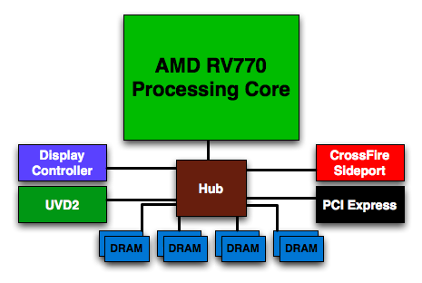
With the ring bus data needed to be forwarded from one ring stop to the next and all clients got access to the full bandwidth, regardless of whether or not they needed it. For relatively low bandwidth data (e.g. UVD2 and display controller data), the ring bus was a horrible waste of power.
With the RV770 all that exists is a simple switched hub, which means that sending data to the display controller, PCIe and UVD2 (AMD's video decode engine) traffic are now far less costly from a power standpoint. Another side effect of ditching the ring bus is a reduction in latency since data is sent point to point rather than around a ring. With the move to a hub, AMD increased their internal bus width to 2kbits wide (which is huge). Maximum bandwidth has increased to 192GB/s (in 4870) but this depends on clock speeds.
With nearly double the internal bandwidth and a point to point communication system, latency between memory clients should be decreased, and huge amounts of data can move between parts of the chip. Certainly getting enough data on to the GPU to feed 800 execution units is a major undertaking and AMD needed to make a lot of things wider to accommodate this.
The CrossFire Sideport
Although AMD isn't talking about it now, the CrossFire Sideport is a new feature of the RV770 architecture that isn't in use on the RV770 at all. In future, single-card, multi-GPU solutions (*cough* R700) this interface will be used to communicate between adjacent GPUs - in theory allowing for better scaling with CrossFire. We'll be able to test this shortly as AMD is quickly readying its dual-GPU RV770 card under the R700 codename.
One thing is for sure, anything AMD can do to assist in providing more reliable consistent scaling with CrossFire will go a long way to help them move past some of the road blocks they currently have with respect to competing in the high end space. We're excited to see if this really makes a difference, as currently CrossFire is performed the same way it always has been: by combining the output of the rendered framebuffer of two cards. Adding some sort of real GPU-to-GPU communication might help sort out some of their issues.
Fixing AMD's Poor AA Performance
Now that we have a new architecture from AMD with improved AA performance, it's time again to look at a comparison of all the different AA modes these cards offer. No new modes have been introduced since the R600 and G80 reviews, but AMD has completely rebuilt their ROPs with special attention to hardware based AA resolve. In R600, hardware resolve wasn't much faster than shader based resolve, but this time around, AA runs blazingly fast whether its on the dedicated resolve hardware or on the shader hardware (since their is so much more shader hardware now even shader based resolve gets a giant boost).
The first thing we will want to look at are the MSAA modes. These are the modes we absolutely recommend for use with AMD hardware as all their other filters essentially low-pass filter the entire image by blending in neighboring subpixels. In any case, the results are very impressive for RV770.
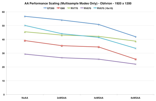
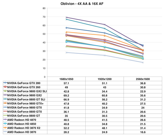
The RV670 at 19x12 was limited in some way other than AA (it really couldn't keep up), but at 16x10 we can get a better idea of relative impact of AA. And clearly the RV770 quite improves fall off with increasing AA levels over the previous generation. One special thing to note is that the RV770 does fall off very gracefully to 8xAA. Since the RV670, G80 and GT200 all have sharp drops in performance when moving up from 4xAA to 8xAA, the RV770 really shines here. In fact, the few tests we did with 8xAA paints the 4870 in a much better light relative to the GTX 280. Remember from our earlier architecture discussion that Oblivion is the game where the GT200 had the largest performance advantage over RV770.
While 8xAA performance is all well and good, the image quality difference is just not enough for us to recommend enabling it over increasing resolution (or better yet, pixel density on LCD panels -- hello display makers). For those with panels that don't go over 1280x1024, it would be better to spend the extra money on a large panel than a $300 graphics card. The application where we see 8xAA making the most sense is on 50+ HDTVs used as computer monitors where the pixels are just plain huge. For the majority of desktop users though 4xAA is where it's at.
We did test the performance of all the other modes as well. NVIDIA's CSAA modes are quite good (they actually improve image quality rather than degrade it), but again, stay away from anything but AMD's "box" filtered AA.
The RV770 actually shows a bigger performance hit from enabling their tent filters than RV670. This is likely because the filters are run on shader hardware in both cases while RV770 has faster hardware resolve that can be used for normal AA resolve. If RV670 resolves "box" filtered AA on the shader as well this would explain the flatter performance in that case. Even more so than the image quality question, the fact that they perform lower really should be the nail in the coffin for AMD's tent filter garbage.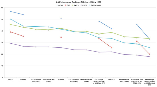
AA Comparison
And now the fun part: playing around with images. Certainly everyone has their own taste when it comes to AA, but we've cropped and blown up this 800x600 screenshot from Oblivion in order to better show what's really going on. As resolution increases and pixel size decreases, the impact of higher AA modes also decreases. This is useful to keep in mind here.
A few key points to check out: compare the interior of textures between either no AA image and any of AMD's tent filters. Notice how the detail on interior textures is significantly decreased. It can be quite frustrating to enable a high anisotropic filtering level to increase the detail of textures only to find them blurred by your AA mode. Also, note how NVIDIA's 8x CSAA and 16x CSAA modes only subtly change some of the pixels. This is because CSAA actually attempts to better understand the actual geometry that a pixel covers rather than going around looking for data outside the pixel to bring in.
These screenshots are with gamma correction enabled on NVIDIA hardware in order to give the best comparison with RV770 which does not allow us to disable gamma correction. We do prefer disabling gamma correction for the average case and especially for anti-aliasing thin lines.
Click the links in the table below to change the AA images displayed


AMD RV770 |
NVIDIA GT200 |
Click here to download all the full resolution, uncompressed images used in this comparison
The Test
| Test Setup | |
| CPU | Intel Core 2 Extreme QX9770 @ 3.20GHz |
| Motherboard | EVGA nForce 790i SLI Intel DX48BT2 |
| Video Cards | ATI Radeon HD 4870 ATI Radeon HD 4850 ATI Radeon HD 3870X2 ATI Radeon HD 3870 EVGA GeForce 9800 GTX KO NVIDIA GeForce 9800 GTX+ NVIDIA GeForce 9800 GTX NVIDIA GeForce 9800 GX2 NVIDIA GeForce 8800 GTX NVIDIA GeForce 8800 GT NVIDIA GeForce GTX 280 NVIDIA GeForce GTX 260 |
| Video Drivers | Catalyst Press Driver (8.7 beta) Catalyst 8.5 ForceWare 177.34 (for GT200) ForceWare 177.39 (for 9800 GTX/9800 GTX+) ForceWare 175.16 (everything else) |
| Hard Drive | Seagate 7200.9 120GB 8MB 7200RPM |
| RAM | 4 x 1GB Corsair DDR3-1333 7-7-7-20 |
| Operating System | Windows Vista Ultimate 64-bit SP1 |
| PSU | PC Power & Cooling Turbo Cool 1200W |
Crysis
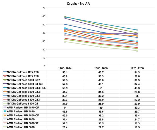
Crysis is a game that can beat down all cards. We're once again using the high settings with the shaders at very high, and even at a fairly tame resolution of 1680x1050 only 8 cards manage to get past the magical 30fps rate, with nearly half of those are just squeaking by. Crysis is particularly punishing on the HD3000 series cards at these kinds of settings, where only the HD3870 X2 was competitive without resorting toCrossfire. This makes the placement of the HD4000 series all the more important.
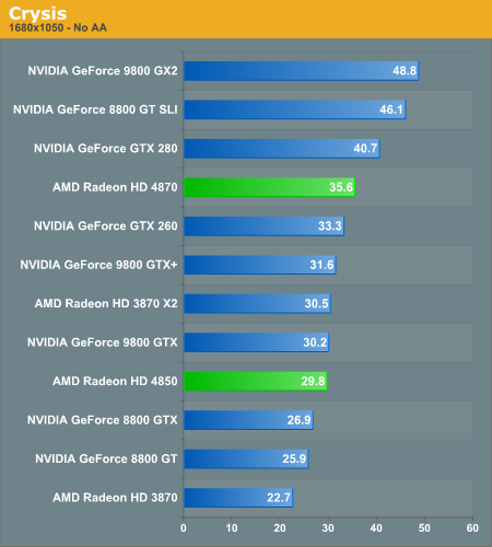
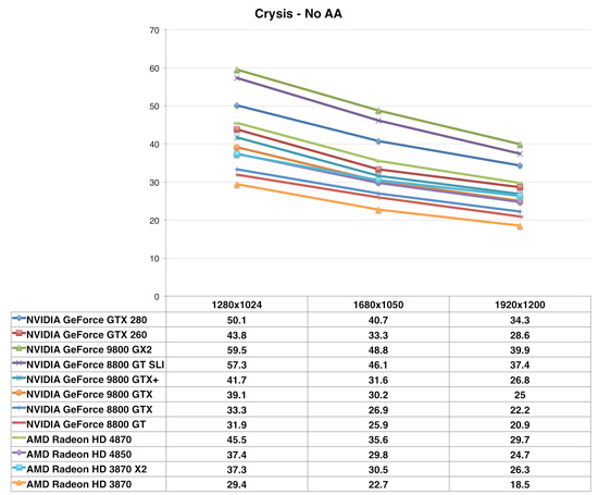
What we see with the 4870 is very promising. Here it leapfrogs the $100 more expensive GTX 260 and delivers 7% more performance at the same time, delivering manageable framerates. It does struggle a bit to separate itself from its cheaper brother the 4850 however, with only a 20% boost in performance for a 50% boost in price. This isn't unexpected of course, it's almost exactly in line with the shader power difference between the two and we've known that this test is shader-bound for some time, but we're not seeing the memory bandwidth make even a slight difference here even at the more unplayable 1900x1200 resolution.
Neither HD4000 card can crack 30fps at higher resolutions however, after 1680x1050 you either need to turn the settings down or start throwing down additional cash for one of NVIDIA's more expensive cards or a Crossfire/SLI solution. In either case, this situation highlights the fact that on a dollar-for-dollar basis, the HD4000 series has negated NVIDIA's commanding lead with Crysis merely two weeks ago.
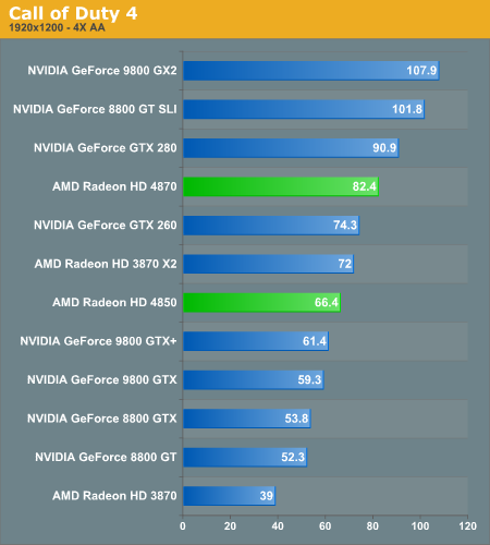
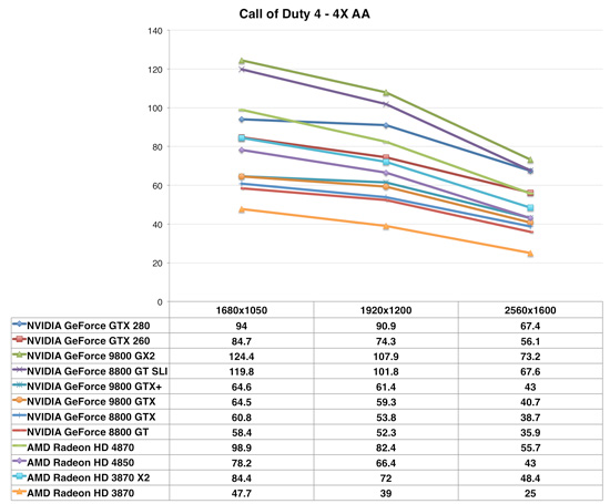
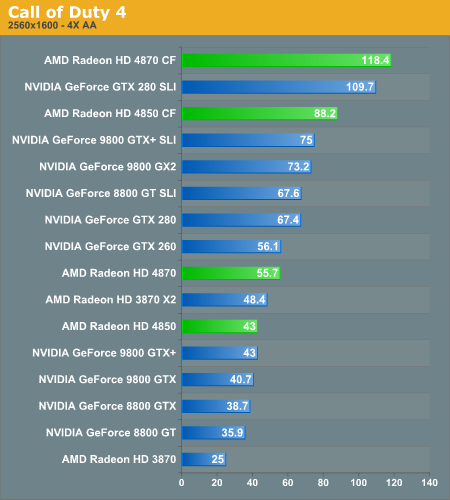
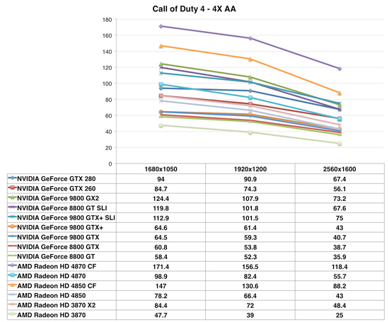
Call of Duty 4
Call of Duty 4 shows the Radeon HD 4870 outperforming the Geforce GTX 260, despite being priced $100 more than AMD's offering. What's interesting is that while at 1920 x 1200 the Radeon HD 4870 is nearly 11% faster than the GTX 260, the two perform the same at 2560 x 1600. It's not a memory bandwidth limitation since the 4870 has tons of it, so it looks like we're running into some sort of a processing power limitation.
The 4870 also nips at the heels of the GeForce GTX 280, but it cannot catch up to the performance offered by two GeForce 8800 GTs in SLI thanks to excellent SLI scaling here. As we've already seen, the Radeon HD 4850 is not only faster than the GeForce 9800 GTX but also the new 55nm GeForce 9800 GTX+.
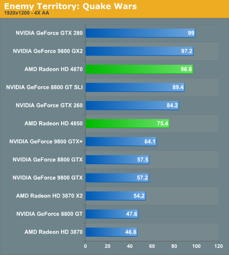
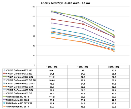
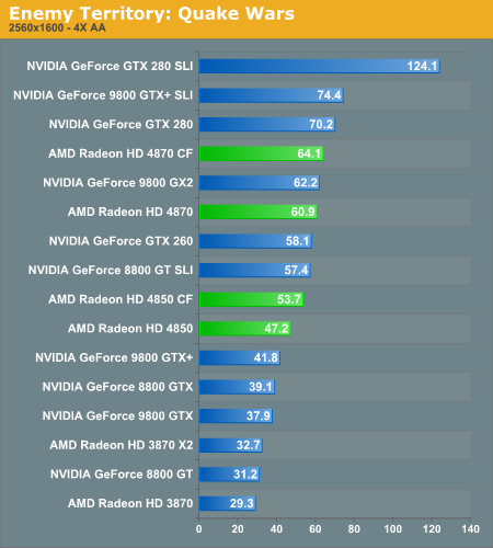
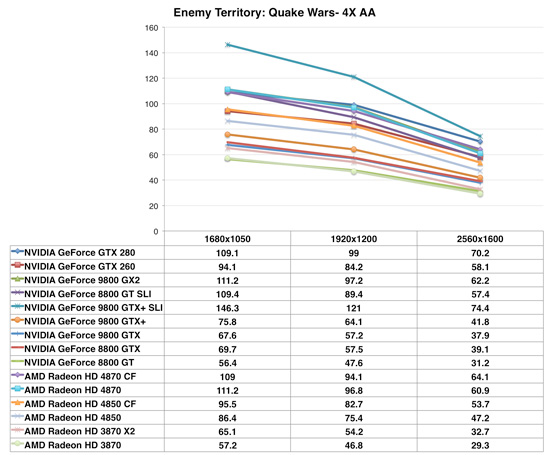
Enemy Territory: Quake Wars
Quake Wars once again shows the 4870 outperforming the GTX 260, but this time it offers essentially the same performance as the GTX 280 - but at half the price. The Radeon HD 4850 also manages to significantly outperform the 9800 lineup.
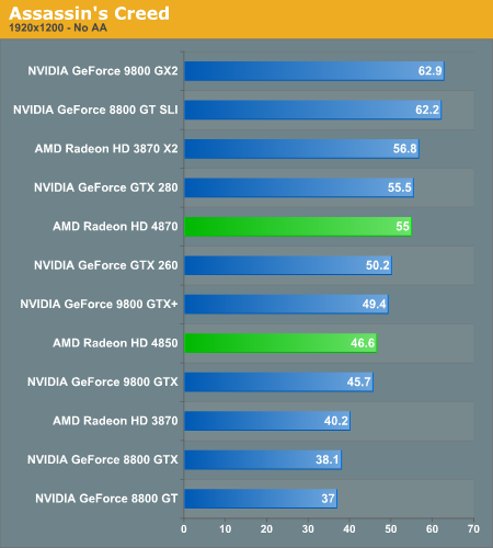
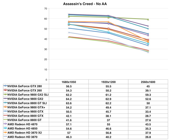
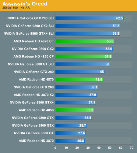
Assassin's Creed
Assassin's Creed is capped at near 60 fps, which is why we see most cards reaching but not significantly exceeding that marker. Performance of the Radeon HD 4870 continues to be strong, but because of the frame rate cap we're not able to see if the GTX 280 could stretch its legs further and eventually outperform the 4870. In actual gameplay, the 4870 and GTX 280 appear to be equals.
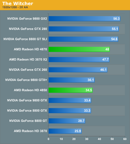
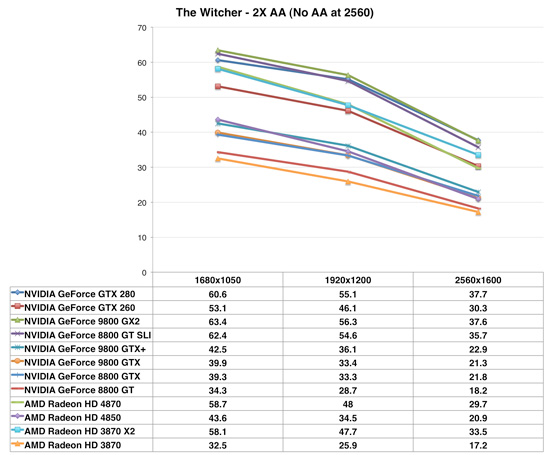
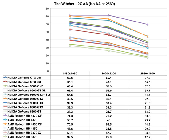
The Witcher
The Witcher continues the trend of the 4870 surpassing the 9800GTX+ by a wide margin and edging out the more expensive GTX 260. It even blows well past its own brother the 4850. Here we see the additional memory bandwidth of the 4870 makes itself very prominent with a 39% boost in performance over the 4850, well beyond just the improvement in core speed. Although both cards offer framerates we'd consider playable at our stock resolution of 1920x1200, the 4870 is definitely the much more comfortable choice, with plenty of headroom for features such as additional anti-aliasing beyond just 2x.
Finally, it's interesting to note that the 4870 and the 3870 X2 are neck-and-neck until we finally crank up the resolution to 2560x1600, at which point the 3870 X2 pulls ahead. This is not what we would have expected. The HD4000 series seems to scale just a bit worse with resolutionthan either NVIDIA's cards or the HD3000 series.
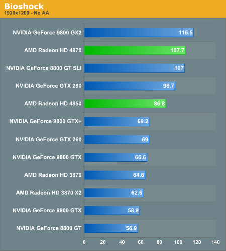
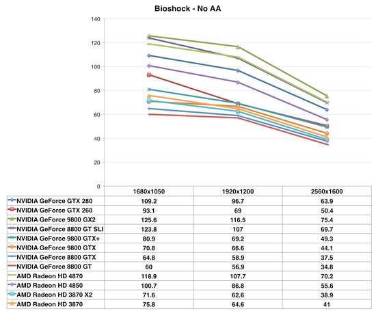
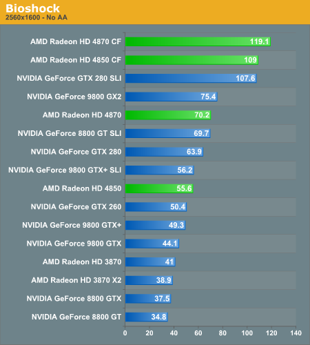
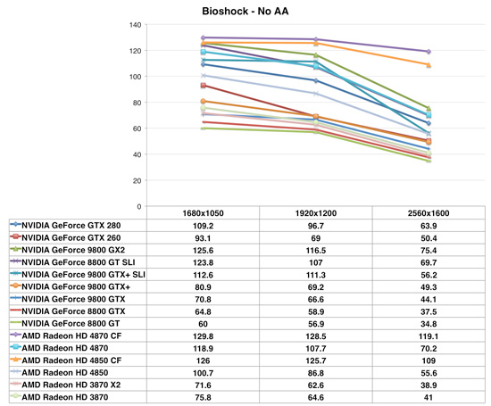
Bioshock
AMD's RV770 GPUs absolutely demolish in Bioshock, the Radeon HD 4850 is nearly as fast as a GTX 280 and the 4870 is close to the speed of a GeForce 9800 GX2.
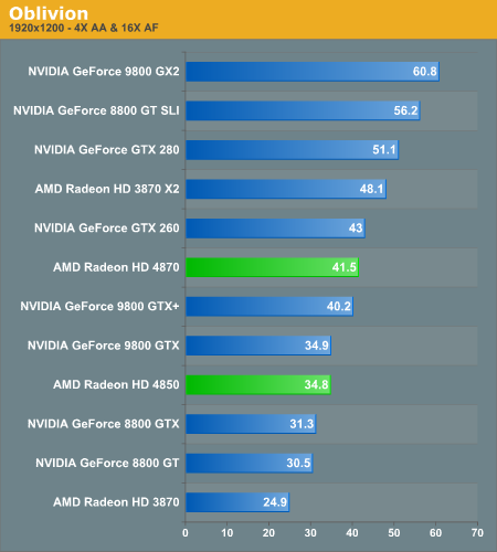
Oblivion
Performance expectations are reset a bit in Oblivion, where the 4870 performs at near the level of a GeForce GTX 260, and the Radeon HD 4850 acts a lot like a GeForce 9800 GTX. Not bad at all, but not the sort of domination we saw in Bioshock. Which just goes to show you that game performance will vary greatly depending on the type of code these GPUs are running.
Multi-GPU Performance
Crysis
NVIDIA's own multi-GPU solution outperformed the GeForce GTX 280 when it launched, so it is not too surprising to see the Radeon HD 4870 in CrossFire mode doing the same. If AMD can put two of these things on a single card it will have a viable competitor for the GTX 280 as well as the GX2.
Call of Duty 4
AMD's architecture did very well under Call of Duty 4 in the single-card tests, with a single Radeon HD 4870 performing better than a GeForce GTX 260. The scaling from one to two cards is beyond perfect in CoD4, the reason being that we test on two different platforms (Intel X48 for CrossFire, NVIDIA 790i for all single-cards), the end result is a rare case where two of AMD's $300 cards actually outperform two of NVIDIA's $650 cards. By no means is it the norm, but it is a testament to the strength of AMD's RV770 GPU.
Enemy Territory: Quake Wars
CrossFire continues to scale poorly in Quake Wars, while NVIDIA's GeForce GTX 280 SLI completely dominates the charts here. The 4870 CF performance isn't terrible, it's actually in line with where it should be (2 x $300 cards are about as fast as 1 x $650 card).
Assassin's Creed
Even at 2560 x 1600 the high end configurations are bumping into a frame rate limiter, any of the very high end setups are capable of running Assassin's Creed very well.
Oblivion
The GeForce 9800 GTX+ does very well in Oblivion and a pair of them actually give the 4870 CF a run for its money, especially given that the GTX+ is a bit cheaper. While it's not the trend, it does illustrate that GPU performance can really vary from one application to the next. The Radeon HD 4870 is still faster, overall, just not in this case where it performs equally to a GTX+.
The Witcher
We've said it over and over again: while CrossFire doesn't scale as consistently as SLI, when it does, it has the potential to outscale SLI, and The Witcher is the perfect example of that. While the GeForce GTX 280 sees performance go up 55% from one to two cards, the Radeon HD 4870 sees a full 100% increase in performance.
It is worth noting that we are able to see these performance gains due to a late driver drop by AMD that enables CrossFire support in The Witcher. We do hope that AMD looks at enabling CrossFire in games other than those we test, but we do appreciate the quick turnaround in enabling support - at least once it was brought to their attention.
Bioshock
The Radeon HD 4000 series did very well in Bioshock in our single-GPU tests, but pair two of these things up and we're now setting performance records.
Power Consumption
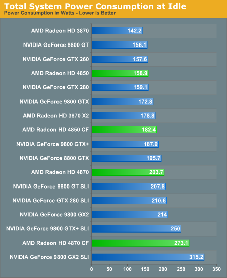
NVIDIA's idle power optimizations do a great job of keeping their very power hungry parts sitting pretty when in 2D mode. Many people I know just leave their computers on all day and generally playing games 24 hours a day is not that great for the health. Idle power is important, especially as energy costs rise, and taking steps to ensure that less power is drawn when less power is needed is a great direction to move in. AMD's 4870 hardware is less power friendly, but 4850 is pretty well balanced at idle.
Moving on to load power.
These numbers are peak power draw experienced over multiple runs of 3dmark vantage's third feature test (pixel shaders). This test heavily loads the GPU while being very light on the rest of the system so that we can get as clear a picture of relative GPU power draw as possible. Playing games will incur much higher system level power draw as the CPU, memory, drives and other hardware may also start to hit their own peak power draw at the same time. 4850 and 4870 CrossFire both require large and stable PSUs in order to play actual games.
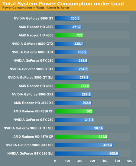
Clearly the 4870 is a power junky posting the second highest peak power of any card (second only to NVIDIA's GTX 280). While a single 4870 draws more power than the 9800 GX2, quad SLI does peak higher than 4870 crossfire. 4850 power draw is on par with its competitors, but 4850 crossfire does seem to have an advantage in power draw over the 9800 GTX+.
Heat and Noise
These cards get way too hot. I keep burning my hands when I try to swap them out, and Anand seems to enjoy using recently tested 4800 series cards as space heaters. We didn't look at heat data for this article, but our 4850 tests show that things get toasty. And the 4870 gets hugely hot.
The fans are kind of quiet most of the time, but some added noise for less system heat might be a good trade off. Even if it's load, making the rest of a system incredibly hot isn't really the right way to go as other fans will need to work harder and/or components might start to fail.
The noise level of the 4850 fan is alright, but when the 4870 spins up I tend to glance out the window to make sure a jet isn't just about to fly into the building. It's hugely loud at load, but it doesn't get there fast and it doesn't stay there long. It seems AMD favored cooling things down quick and then returning to quiet running.
Final Words
Due to circumstances quite beyond our control, this will be essentially the third time we've covered the Radeon HD 4850. AMD has managed to make the $200 price point very exciting and competitive, and the less powerful version of RV770 that is the 4850 is a great buy for the performance.
As for the new business, the Radeon HD 4870 is not only based on an efficient architecture (both in terms of performance per area and per watt), it is an excellent buy as well. Of course we have to put out the usual disclaimer of "it depends on the benchmark you care about," but in our testing we definitely saw this $300 part perform at the level of NVIDIA's $400 GT200 variant, the GTX 260. This fact clearly sets the 4870 in a performance class beyond its price.
Once again we see tremendous potential in CrossFire. When it works, it scales extremely well, but when it doesn't - the results aren't very good. You may have noticed better CrossFire scaling in Bioshock and the Witcher since our Radeon HD 4850 preview just a few days ago. The reason for the improved scaling is that AMD provided us with a new driver drop yesterday (and quietly made public) that enables CrossFire profiles for both of these games. The correlation between the timing of our review and AMD addressing poor CF scaling in those two games is supicious. If AMD is truly going to go the multi-GPU route for its high end parts, it needs to enable more consistent support for CF across the board - regardless of whether or not we feature those games in our reviews.
That being said, AMD's strategy has validity as we've seen here today. A pair of Radeon HD 4850s can come close to the performance of a GeForce GTX 280, and a pair of Radeon HD 4870s are faster across the board - not to mention that they should be $50 less than the GTX 280 and will work on motherboards with Intel-chipsets. Quite possibly more important than the fact that AMD's multi-GPU strategy has potential is the fact that it may not even be necessary for the majority of gamers - a single Radeon HD 4850 or Radeon HD 4870 is easily enough to run anything out today. We'll still need the large monolithic GPUs (or multi-GPU solutions) to help drive the industry forward, but AMD raised the bar for single-card, single-GPU performance through good design, execution and timing with its RV770. Just as NVIDIA picked the perfect time to release its 8800 GT last year, AMD picked the perfect time to release the 4800 series this year.
Like it's RV670 based predecessors, the Radeon 4850 and 4870 both implement DX10.1 support and enable GPU computing through their CAL SDK and various high level language constructs that can compile down SPMD code to run on AMD hardware. While these features are great and we encourage developers to embrace them, we aren't going to recommend cards based on features that aren't yet widely used. Did we mention there's a tessellator in there?
On the GPGPU side of things, we love the fact that both NVIDIA and AMD are sharing more information with us, but developers are going to need more hardware detail. As we mentioned in our GT200 coverage, we are still hoping that Intel jumping in the game will stir things up enough to really get us some great low level information.
We know that NVIDIA and AMD do a whole lot of things in a similar way, but that their compute arrays are vastly different in the way they handle single threads. The differences in the architecture has the effect of causing different optimization techniques to be needed for both architectures which can make writing fast code for both quite a challenge. The future is wide open in terms of how game developers and GPGPU programs tend to favor writing code and what affect that will have on the future performance of both NVIDIA and AMD hardware.
For now, the Radeon HD 4870 and 4850 are both solid values and cards we would absolutely recommend to readers looking for hardware at the $200 and $300 price points. The fact of the matter is that by NVIDIA's standards, the 4870 should be priced at $400 and the 4850 should be around $250. You can either look at it as AMD giving you a bargain or NVIDIA charging too much, either way it's healthy competition in the graphics industry once again (after far too long of a hiatus).


