Original Link: https://www.anandtech.com/show/2482
NVIDIA's 790i Arrives: SLI Rides Again
by Kris Boughton on March 18, 2008 9:00 AM EST- Posted in
- CPUs
Watch out Intel - NVIDIA's just broken out the big guns and this time they're not holding anything back. Coming out firing with both barrels blazing, the nForce 790i (Ultra) SLI promises to provide users with the ultimate platform for high-intensity, adrenaline-pounding gaming when it comes to combining NVIDIA multi-GPU 3D graphics and the power of today's most advanced Intel desktop microprocessors. Probably sounds a little over the top, but this time we reckon an nForce chipset for the Intel platform will live up to the hype.
Aiming to steal as much attention as possible from the ongoing coverage of the many looming product releases based on Intel's upcoming X48 Express chipset, 790i makes no apologies for what it is: one of the fastest gaming platforms we have ever tested. In the past, less than impressive processor and memory overclocking capabilities - especially when running data-hungry quad-core CPUs - made it difficult to recommend an NVIDIA-based system to anyone other than those looking for the absolute maximum in gaming performance. After spending sometime with the nForce 790i Ultra SLI motherboards from ASUS and EVGA, we're not so sure we can say that anymore.
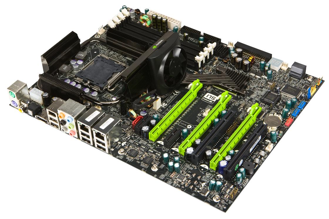 A familiar color combination makes a comeback with NVIDIA's latest offering. EVGA's mean n' green NVIDIA nForce 790i Ultra SLI promises to take your gaming experience to a whole new level. |
Much like we have seen in the past, the initial NVIDIA offerings will consist of near immediate, worldwide product availability from the usual suspects - EVGA and XFX - as well as a few non-reference designs from vendors such ASUS, DFI, Gigabyte and MSI. For instance, we have the ASUS Striker II Extreme, which fortunately landed in our hands a little earlier this month allowing us additional time to test this platform. Squarely targeted at the serious gamer and extreme benchmarking enthusiast looking to squeeze every last ounce of 3D performance from their systems, motherboards based on 790i are the next big step in NVIDIA's quest for absolute dominance in the discrete graphics marketplace.
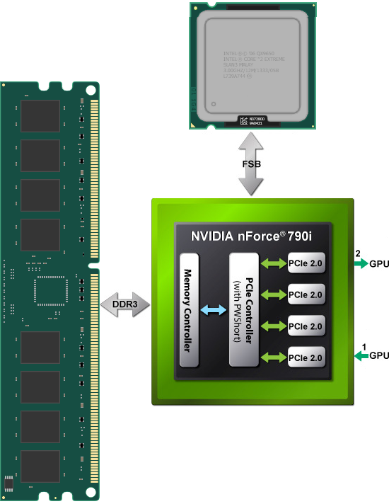
The NVIDIA nForce 790i SLI chipset is comprised of two parts. First is the System Platform Processor (SPP), analogous to Intel's Memory Controller Hub (MCH) or "Northbridge", and second is the Media and Communications Processor (MCP) that provides nearly the same functionality as Intel's I/O Controller Hub (ICH) or "Southbridge." Together these processors form the foundation needed to experience the very latest in NVIDIA multi-GPU SLI technology. Current 780i-based motherboard owners should note with approval the absence of the nForce 200 sub-processor from this line-up as the functionality (PCIe 2.0) formerly provided by this chip is now natively supported by the improved 790i SPP. As a side note, the nForce 200 is nearly the same chip employed on Intel Skulltrail motherboard, which allows enabling SLI-accelerated graphics. (Skulltrail uses the nForce 100, a first generation part that supports only PCIe 1.x link speeds.)
 NVIDIA's nForce 790i Ultra SLI specifications are shown here. The 790i SLI block diagram is strikingly similar; the only difference is a reference to JEDEC 1333MHz memory support and not the DDR3-2000 overclock capability highlighted above. |
The SPP contains bus control logic required to interface with the Central Processing Unit (CPU) via Intel's now well-aged Front Side Bus (FSB) in addition to a single, scalable HyperTransport Technology (HTT) link - licensed for use from AMD - which interfaces with the MCP. One of the major changes over the 780i SLI MCP is the integration of NVIDIA's newly-designed DDR3 memory controller capable of addressing up to 8GB of unregistered, non-ECC DDR3 memory. Add to this the incorporation of complete PCI Express (PCIe) 2.0 bus support and we can see that 790i is more than just a simple upgrade from 780i. Those looking to swap their current board for one featuring the 790i should find more than enough reason to consider the change.
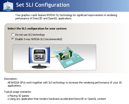
In order to retain their platform's competitive edge, NVIDIA has pulled out all the stops. They provide the required next-generation 45nm Intel LGA775 dual-core and quad-core CPU compatibility with official FSB 1600 support. Beyond that, we get DDR3 with EPP2 and two x16 PCIe 2.0 slots along with a third providing an additional full x16 PCIe 1.x link for second-generation tri-SLI graphics acceleration. Quad-SLI (using two GeForce 9800 GX2 cards) is also supported. Finally, the platform provides a tight integration of on-the-fly system control and monitoring courtesy of the Enthusiast System Architecture (ESA).
We will be taking an in-depth look at the 790i based ASUS Striker II Extreme shortly and providing a full benchmark test suite with comparisons to other NVIDIA chipsets. As for today, let's take a closer look at what the new nForce 790i platform has in store for the serious gamer and overclocker - besides the cost of a new motherboard and a kit of expensive DDR3 performance memory.
nForce 790i MCP Configurations and EVGA Board Specifications
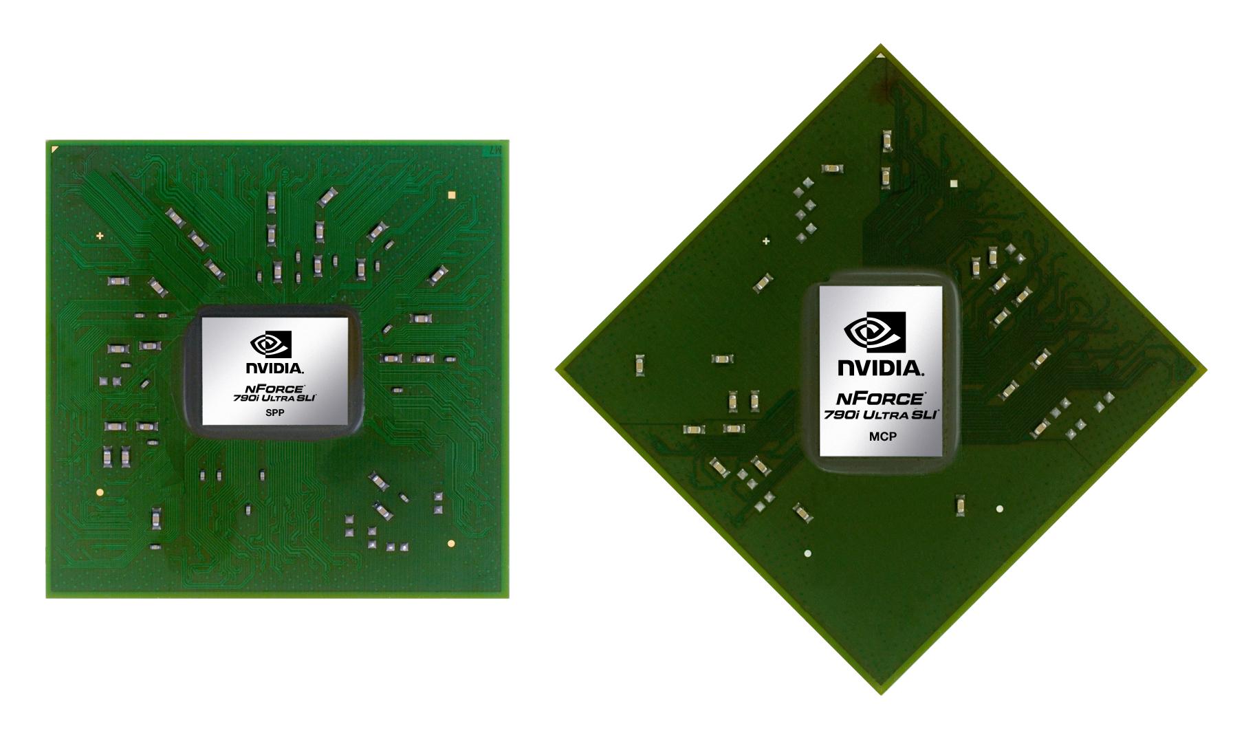 Both the 790i SLI SPP and MCP are built using relatively outdated 90nm process technology. Like Intel's latest chipsets, they are long overdue for a shrink to 65nm. |
It's worth noting that, unlike past releases, NVIDIA's top-end nForce 790i SLI SPP will be available to motherboard vendors in two distinct flavors; a new "Ultra" version will be the new top-end part. While NVIDIA claims that both versions are sure to be highly overclockable, the 790i SLI Ultra targets extreme overclocking and will feature automatic configuration of memory for DDR3-2000 operation using EPP2 profiles built into SLI-ready memory modules. Suppliers looking to offer products featuring slightly less aggressive CPU and memory overclocking capabilities for those on a tighter budget will use the "standard" 790i SLI part. Be sure to pay close attention to this important distinction when shopping for your next board. The chips are almost certainly the same internally, but the Ultra parts are binned for higher performance, similar to what we see with CPUs and more recently with the X38 and X48.
No matter the SPP used, the 790i SLI MCP is the same in either implementation. In fact, our investigation has revealed the aptly-named 790i SLI MCP as nothing more than a re-worked 570i SLI MCP with a stepping change to A3. This left us wondering if NVIDIA's been experiencing design issues with their newest creation, causing delays with its release, or if they just had a hard time convincing themselves of the necessity for something better. In either case, there is little room to complain - we feel the included MCP is more than capable of satisfying our needs as is and anything more would have just driven up the cost in exchange for no real benefit.
| EVGA NVIDIA nForce 790i Ultra SLI | |
| Market Segment | High-Performance Gaming / Extreme Benching - $349.99 (estimated) |
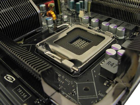
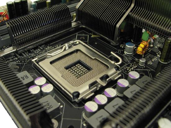
| CPU Interface | Socket T (LGA775) |
| CPU Support | LGA775 Core2 Duo/Extreme/Quad, Pentium EE, Pentium D, Pentium including next-generation 45nm CPU support |
| Chipset | NVIDIA nForce 790i Ultra SLI SPP and MCP |
| CPU Clock Multiplier | 6x ~ 11x, downward adjustable for Core2, upward to 60x for Core2 Extreme, including half-multiplier support for 45nm processors |
| FSB Speeds | Auto, installed CPU Default to 700MHz in 1MHz increments |
| System Bus Speeds | 1600 / 1333 / 1066 / 800 MHz |
| FSB Memory Clock Modes | Auto, Linked, Unlinked |
| DDR3 Memory Ratios | Auto, 5:4, 3:2 and Sync Mode (2:1) |
| PCIe Speeds | Auto, 100MHz ~ 200MHz in 1MHz increments |
| SPP-to-MCP Link Speeds | Auto, 200 ~ 500Mhz in 0.5MHz increments to 210MHz then 1MHz steps |
| HT Multipliers | 1x ~ 5x for SPP->MCP and MCP->SPP |
| EPP 2 Profile Support | Enabled (DDR3-2000 set), Disabled |
| DRAM Timing Controls | Optimal, Expert (tCL, tRCD, tRP, tRAS and CPC user adjustable) |
| Advanced Memory Settings | Auto or user adjustable - tRRD, tRC, tWR, tWTR, tFAW and tREF |
| DRAM Command Per Clock | Auto, 1T, 2T |
| CPU Core Control | Enabled, Disabled for each core (excluding Core 0) |
| CPU Core Voltage | Auto, 0.51250 ~ 2.00000 in 0.00625V increments |
| CPU FSB Voltage (VTT) | Auto, 1.10V ~ 1.45V in 0.05V increments |
| Memory Voltage | Auto, 1.50V ~ 2.275V in 0.025V increments |
| nForce SPP Voltage | Auto, 1.30V ~ 1.55V in 0.05V increments |
| nForce MCP Voltage | Auto, 1.50V ~ 1.75V in 0.05V increments |
| GTLVREF Lane Voltages | Auto, -155mV ~ +155mV for each GTL reference voltage |
| Memory Slots | Four 240-pin DDR3 DIMM Slots Dual-Channel Memory Architecture Regular Unbuffered, non-ECC DDR3 Memory to DDR3-1333, 8GB Total Supports SLI-Ready EPP 1/2 Memory to DDR3-2000 |
| Expansion Slots | 2 - PCIe 2.0 x16, Supports up to NVIDIA 3-way SLI Technology 1 - PCIe (1.x) x16 2 - PCIe (1.x) x1 2 - PCI Slot 2.2 |
| Onboard SATA RAID | 6x SATA 3.0Gbps Ports - nForce MCP (NVIDIA MediaShield RAID 0, 1, 0+1, 5 and JBOD) |
| Onboard IDE/Additional SATA | JMicron JMB363 PATA Controller (up to 2 UDMA 133/100/66 devices) Up to 6 External eSATA ports configurable via BIOS |
| Onboard USB 2.0/IEEE-1394 | 10 USB 2.0 Ports - (6) I/O Panel, (4) via headers 2x 1394a Ports - (1) I/O Panel, (1) via header |
| Onboard LAN (with Teaming) |
Dual NVIDIA nForce LAN with DualNet and FirstPacket Technology |
| Onboard Audio | 8-channel HD Audio (Azalia) CODEC |
| Power Connectors | ATX 24-pin, 8-pin EATX 12V |
| I/O Panel | 1 x PS/2 Keyboard, 1x PS/2 Mouse 2 x SPDIF - (1) Optical Out, (1) Coaxial Out 1 x External eSATA 2 x IEEE-1394a port 2 x RJ-45 (LAN) 6 x USB 2.0/1.1 8 channel Audio IO |
| Fan Headers | 6 - (1) CPU, (1) nForce SPP fan (optional), (4) Chassis |
| BIOS Revision | P03_R2 (pre-release) |
The BIOS has matured quite well since 780i, although when compared to most feature-rich enthusiast-level Intel-based motherboards the interface can appear a little barren. For one, Intel chipsets still expose a far greater set of memory control timings, depending on whose motherboard you purchase. While we are all for best matched values and the deliberate use of autonomous optimization control routines when it comes to BIOS setup, we also acknowledge the importance of giving the user a little rope with which to hang themselves if they so chose. In our eyes, the solution is quite simple: provide as much interface as possible to the user but always leave the option to select "Auto" so that the BIOS can retain primary control of said parameter.
FSB choices are available all the way up to 700MHz (2.80GHz quad-pumped) although we were only able to push our board as high as about 575MHz FSB with a 45nm dual-core E8500. As with 780i, 790i provides the option to either run the memory in sync with the FSB, using one of three predefined memory-to-FSB ratios, or unlinked allowing for nearly any FSB and memory speeds to be selected independently of each other and without any restriction. However, running memory unlinked from the FSB can leave a lot of performance on the table. For this reason alone we suggest you stick with "Sync Mode" and use either the 5:4, 3:2 or 2:1 (best) divider with your DDR3 memory unless you absolutely cannot find a way to make your system perform as expected with one of those settings. We will be covering memory performance - in particular read, write, copy and latency access times - in more detail a little further along in the review.
Voltage selection ranges are good without offering too many obnoxiously high settings - CPU voltage tops out at 2V and DDR3 can be set as high as 2.275V. The remaining voltages - CPU FSB Voltage, nForce SPP Voltage, and nForce MCP Voltage - can be left on auto in most instances, even when overclocking. NVIDIA validation engineers have done an exceptional job of testing the capabilities of their chipset way beyond normal specifications and have passed on their findings via the BIOS. As you increase FSB, the board automatically selects the right voltage needed to POST and run stable. During the course of our testing, we found the board did most of the work for us, making overclocking our system an absolute breeze. All we really needed to do was analyze performance at each configuration and decide which one we thought was best.
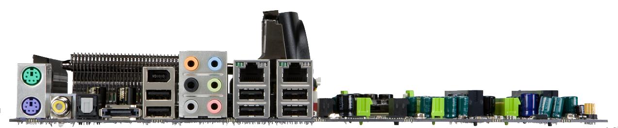 |
Many of the same connections found on EVGA's 780i reference motherboard make a second appearance on their 790i board. Just about everything you might possibly need can be found here - one PS/2 port each for mouse and keyboard (great for those out there that still like to make use of old-style KVM dongles), one 1394a FireWire port, six USB 2.0 ports, dual RJ-45s for the integrated LAN, and audio output jacks for the onboard 8-channel HD Codec. New with the 790i board is the single eSATA header, which can be configured from the BIOS as any one of the six channels available via the MCP, and an SPDIF digital coax audio jack in addition to the optical out.
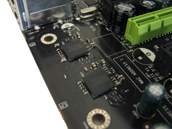
As expected, the 790i SLI MCP provides expansion capabilities for up to six SATA devices and two PATA devices with MediaShield Technology, 10 USB 2.0 devices, and up to five PCI slots. The MCP also allows for up to two 1Gbps (1000Mbps) Ethernet connections including DualNet Technology - used to team adapters to form a single, virtual 2Gbps link - and NVIDIA's FirstPacket Technology, which provides latency-sensitive network transfers, such as giving outgoing gaming traffic priority over bulk-transfer communications like file uploads. The 790i SLI MCP also includes support for onboard high-definition (HD) audio, previously code-named Azalia, and can output a 7.1 analog signal to individually attached speakers as well as an 8-channel SPDIF source via digital coax or optical connection.
EVGA NVIDIA nForce 790i Ultra SLI Board Layout and Features
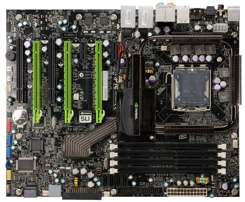 |
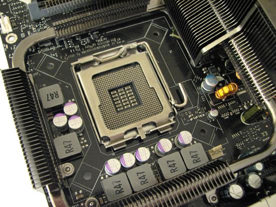
EVGA's NVIDIA nForce 790i Ultra SLI motherboard is vaguely reminiscent of their 780i-based product. The first thing you may notice is the size and location of the chipset cooler. Because the 790i SLI SPP now includes native PCIe 2.0 support, the nForce 200 sub-processor included with the 780i SLI SPP is no longer present; removal of this chip provides just enough extra room to move the SPP up and out of the way of an additional PCIe x1 slot seen closest to the backplane. Unfortunately, the added PCIe slot is non-functional when all three x16 lanes are populated with cards. Although the nForce 790i MCP provides up to 60 PCIe 1.x and 2.0 lanes between the SPP and MCP, link configurations rules do not allow for anything more than the cards needed to run 3-way SLI. Those that wish to run their favorite discrete sound card may find themselves out of luck depending on how they fill their expansion slots.
Microprocessor load current profiles have changed to the point that the use of single-phase regulators is no longer a viable option. Nowadays, designing a cost-effective, thermally-sound, and efficient voltage regulator module (VRM) capable of supporting stable, high-speed CPU operations has become a challenge that can only be accomplished through the use of multi-phase converters. However, the consensus amongst most users seems to be that a greater phase count generally results in better, cleaner power delivery - a fallacy which some industry leaders, motherboard vendors, and technical marketing managers are all too willing to promote.
If fact, we submit to you that it's much easier (and cheaper) to slap a few more power delivery phases on a motherboard than it is to create an actual high-performance solution. The quality of a particular power delivery system is primarily dependent on the overall robustness of the design. Design considerations include proper power and ground plane placement; effective signal routing and decoupling measures; selection, location and rated capacity of correctly matched components; and the overall adherence to sound engineering principles. Because of this, the proper design and implementation of a well-developed 5-phase solution can often outperform a lesser 8-phase solution.
The EVGA 790i also uses a true 6-phase PWM controller, where many other boards may make use of 4-phase controllers designed in such a way as to appear to be native 8-phase solutions. Supply-side capacitance has been significantly increased and the main +12V input capacitance has gone way up from only 470uF to 2000uF. This helps overclocking as some cheaper PSUs have higher allowable tolerances when it comes to input current ripple. We say this knowing full well that beyond a certain point additional capacitance matters very little. Often times larger capacitors are used in order to take advantage of their lower equivalent series resistance (ESR), a specification that has a great deal to do with how quickly the capacitor can react to sudden load changes and provide current precisely when needed.
| Motherboard PWM Comparison | ||||
| Intel Spec |
780i | 790i | Notes | |
| Loadline (mohm) | 1 +/- 0.1 | 0.93 | 1.01 | Higher loadline values create more droop |
| Max Icc (A) | 125 | 165 | 220 | High current output supports higher overclocks |
| Max Overvoltage (V) | 1.6 | 1.8 | 2.0 | Higher voltages allow for extreme overclocking |
| Output Ripple (mV) | 10p-p | 9p-p | 6p-p | Less peak-to-peak ripple means "cleaner" power and more stable overclocks |
| Thermal Drift (mV) | +/- 4 | +/- 3 | +/- 2 | Tighter tolerances means that the circuit is less susceptible to variations in component temperatures |
| Phase Jitter (ns) | no spec | 390 | 180 | Less jitter means smoother, more stable power delivery |
| Efficiency | 75% | 82.4% | 83.6% | Higher efficiency allows for cooler components at higher currents and less energy used by the system |
We have listed a few of the more important PWM specifications in order to compare the differences between the 780i and 790i processor power systems. These are just a couple of the more measurable improvements made to ensure ample processor power delivery under even the most demanding situations and to help minimize the detrimental effects of supply-line switching noise and de-stabilizing output ripple. Overclocking places tremendous demands on the power delivery system and without this strong foundation, even your best efforts are sure to fail (particularly in the case of long-term overclocking).
NVIDIA also recognized the need for a more capable power subsystem cooling solution due to the tremendous current draw of 45nm CPUs experienced during aggressive overclocking. The heatpipe has been extended to encompass both sets of MOSFET banks, including an extra segment of fins used to close the circle and provide additional surface area for maximum heat dissipation. The heatsink assembly is made entirely of aluminum, except for the steel casing used to hold it together, and the included fan can be used to provide active cooling when pushing the board to its absolute limits. The fan speed can also be manually adjusted in the BIOS if you find the whine at full-speed to be a little over the top.
EVGA NVIDIA nForce 790i Ultra SLI Board Layout and Features (Cont'd)
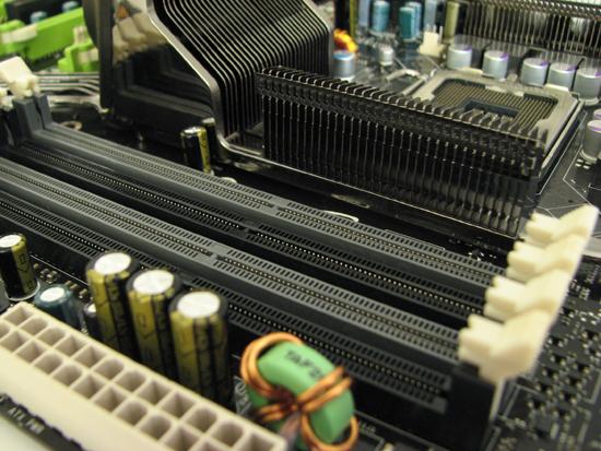
The four DDR3 DIMM slots have been moved slightly down the board in an effort to locate them as close as possible to the 790i SLI SPP, minimizing memory data and control signal trace lengths. Considerations such as these are crucial to the development of memory subsystems with enough signal transfer margin to support data transfer rates well in excess of standard DDR3 specifications. The use of DDR3 also removes the need for an array of onboard termination resistors and frees-up valuable board space for things like additional control transistors, improved copper pours for ground and power plane placement, extra bulk capacitance, and the freedom to more intelligently optimize signal routing wherever possible. If fact, much of the additional speed realized through the use of DDR3 over DDR2 is due to improvements in the interface specifications more than in actual modifications to the memory die architecture. High-speed data systems are especially susceptible to issues like crosstalk and inductive coupling between parallel data lines, which is one of the reasons why most interfaces are rapidly moving away from parallel buses in favor of low pin count serial connections.
Although not shown here, final-shipping retail boards will make use of two separate DIMM slot colors - grey and black. The two black slots, the second and farthest from the CPU socket, should be primary utilized when overclocking memory above 1800MHz. Above this frequency where it matters most, trace lengths have been carefully matched to some of the internal chipset latencies and timings associated with bank addressing in order to provide maximum signal margin. This translates to better memory overclocks, all without the need for excessive VDDQ voltages that are otherwise needed to force operation at these speeds.
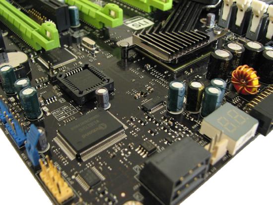
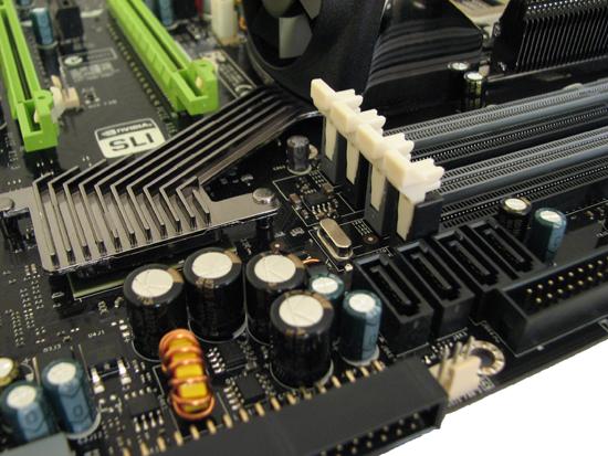
All of the optional USB and 1394a expansion headers are now conveniently located along the bottom edge of the board, unlike past layouts that seem to scatter them to the wind. This also includes the POST status indicator, which was sometimes difficult to view on the 780i board depending on what cards were installed. The same momentary tactile switches for power and reset have also made a comeback, a feature we made extensive use of during our bench testing marathons. The locations of the fan headers also make a lot more sense now. One of the two fan headers grouped at the bottom of the 780i board near these switches has also made a move up the PCB to the back plane area. We really like this as it means we no longer have to decide between running the included chipset fan or a 120mm fan mounted at the back of our case.
Finally, we would be negligent not to mention the placement of an additional SATA port, seen just above the top PCIe x1 slot. This is perfect for those out there that either install a SATA-to-eSATA port adapter or want the ability to run a single deep-storage drive when a 6-disk RAID 5 array occupies every other SATA port hanging off the MCP. It's clear that NVIDIA has partnered well with EVGA and put a lot of thought into improving their latest product.
"PWShort" and "Broadcast" Communication Technologies
The NVIDIA nForce 790i (Ultra) SLI chipset will introduce a couple new data transfer technologies created in order to reduce some of the typical latencies experienced by GPU-to-GPU communications and generally improve bandwidth utilization whenever possible. "Posted-Write Shortcut" (PWShort) and "Broadcast" allows NVIDIA-based system with multiple GPUs to accelerate some of the standard functionality that has, in some configurations, resulted in performance bottlenecks.
Posted-Write Shortcut

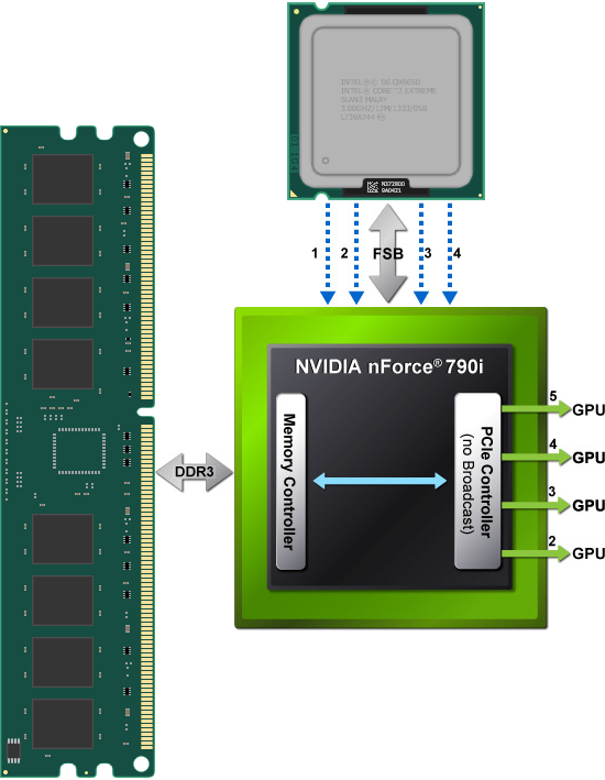
In a 2-way SLI configuration, with the cards installed in the two PCI Express 2.0 slots, the 790i SPP handles the routing of some portion of the traffic between each GPU as well as requests for access to main system memory and communications to and from the CPU. Traffic can also be relayed between cards by way of the SLI bridge. Typically, data sent from one GPU to the other would travel by way of the PCIe controller. This would forward the packet on to the memory controller where the message would be decoded, parsed, and eventually returned to the PCIe controller for final disposition. This is a somewhat inefficient use of both memory controller and PCIe controller resources, not to mention the need for a tremendous amount of additional bandwidth needed to support what should be a simple GPU-to-GPU transfer.
The nForce 790i SPP now includes the ability to peek inside each data packet coming from any device serviced by the chipset's PCIe controller; it can then forward the message directly to its final destination if the intended target is indeed the tandem GPU. Most of these types of communications are data transfers required to keep the two cards' frame buffers synchronized so that each GPU is always reading and modifying the most recent video information. The improved point-to-point data interface made possible by PWShort technology acts to greatly reduce the latency of these types of transfers and ensure more efficient use of the memory-to-PCIe controller link resources.
Broadcast
With systems containing multiple GPUs, the CPU often needs to send the same data to each GPU - for example, when texture, geometry, or other common rendering data must be transfer over the FSB, ultimately intended for receipt by all GPUs. Normally the CPU must send a separate set of data packages in order to target each GPU. This causes FSB congestion due to the increased CPU-to-GPU traffic, which could be better used for other purposes such as main memory read or write requests or cache coherency with quad-core CPUs.
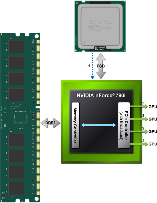
In addition to the direct link technology previously explained, Broadcast technology allows only one message to be sent by the CPU where it is then received, replicated, and broadcasted to all GPUs, eliminating the need for multiple, near-identical transfers over the FSB. This allows for more timely access to other resources that must share this common interface. We're not exactly sure how the SPP can control what the CPU does and does not send over the FSB, and it seems likely that the system drivers also have changes to accommodate this new technology; either way, there's definitely more to this than we have shared so far. We will be sure to pass along anything we learn.
790i users with single GPU systems should not see any appreciable gains due to these new technologies. In both cases, they are aimed at improving communication efficiencies associated with multi-GPU configurations. It's also difficult for us to quantify exactly what kind of impact these new features have on overall system performance. Isolating and attributing gains to either of these innovations is exceedingly difficult, since we can't just turn these features on and off at whim. While 2-way SLI stands to benefit, we can't help but think the PWShort and Broadcast technologies stand to benefit 3-way and 4-way SLI configurations even more; perhaps we will see better scaling with additional GPUs on 790i.
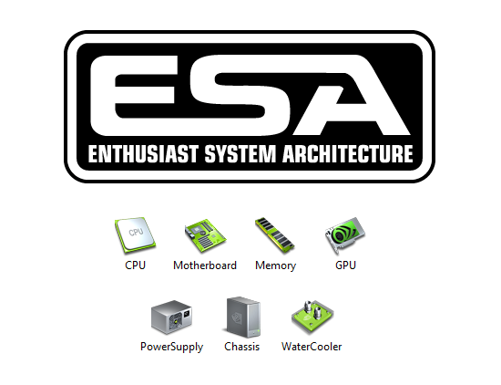
Enthusiast System Architecture and the Improved NVIDIA Control Panel
Enthusiast System Architecture (ESA) is NVIDIA's answer to the absence of a unified status collection and reporting protocol when it comes to monitoring all the components that go into one of today's advanced gaming systems. More than just a proprietary technology, NVIDIA envisions ESA as the next-generation, royalty-free industry standard for peripheral control and monitoring. NVIDIA hopes that by creating an open-standard interface and making it free for use there will be little resistance to the rapid, widespread adoption by all. By layering their logical data transport system on top of USB's physical link system, they can all but guarantee that every motherboard manufactured today is capable of connecting any component supporting ESA.
ESA-certified components are just now beginning to appear on the market, with companies like Cooler Master, OCZ Technologies, Tagan, Thermaltake, and CoolIT Systems leading the charge.
NVIDIA's new Control Panel and System Monitor package exposes nearly every aspect of system control, including all of the same tuning options normally only available for manipulation by restarting and entering the BIOS. Of course, many of these features require that your particular motherboard make and model support NVIDIA's Dynamic BIOS Access. Unfortunately this tool does not invalidate the need to reboot after adjusting many of the options like memory timings, certain voltages, link speeds, and the CPU multiplier; at least the interface is pleasant to work with and easy to navigate. Any changes made here are saved to CMOS and remain in effect until later modified or reset to default.
This monitoring suite uses a 2D/3D hybrid GUI capable of displaying real-time status for each selected component. It conducts XML data logging and allows for arming/disarming of user-adjustable alerts for nearly every system event imaginable. For example, an ESA-certified chassis could report the duty cycle of each case fan, in percent of full speed, while a PSU could do the same for input and output current, calculated efficiency, internal unit temperature, fan speed in RPM, and the actual voltage of each supply rail.
A convenient feature of the Control Panel is the ability to create rules. These rules can be used to define certain component behaviors based on other variable sensor input. For instance, radiator fans used in conjunction with a water-cooled system could be set to speed up or slow down depending on the current measured coolant temperature. This would allow for automatic control of other system temperatures, permitting additional cooling needed to maintain stability during performance workloads while simultaneous minimizing fan noise whenever possible.
Rules can then be grouped together with specific component settings to form custom profiles. Each of these can tailor key system characteristics depending on the types of operations being performed. Thus it becomes possible to quickly move between pre-established configurations best suited for the manner in which the system will be used - whether that's watching a DVD movie in a quiet environment, playing your favorite online first-person 3D shooter, or chatting with your friend half-way around the world. With customizable rules associated with individual profiles there's practically no limit to what users can accomplish.
CPU Overclocking Capabilities: The 45nm E8500 and QX9770 Exposed
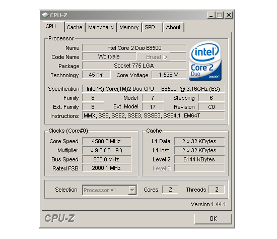
Whatever the 780i may have lacked when it came to overclocking 45nm CPUs certainly does not apply to 790i. Achieving a stable 4.5GHz overclock using an E8500 was no problem at all for the EVGA board. Gaming at these speeds promises to be incredibly fast. This kind of overclock required water-cooling for the CPU, so be sure to upgrade your cooling if you want any chance of reaching these frequencies and retaining stability.
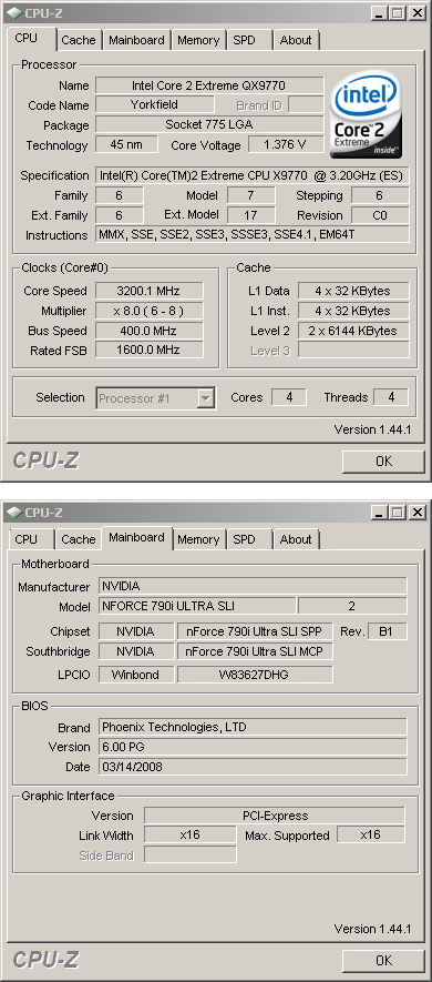
The EVGA 790i Ultra also handled our QX9770 sample with relative ease. We were able to benchmark and play games without incident at 400MHz FSB, our mark of excellence when it comes to quad-core overclocking. Tuning memory for DDR3-1600 operation at this speed using a 2:1 divider and 7-7-7-22 or even 6-6-6-18 timings is quite fast. Unlike other Core2 Duo's, the QX9650 and QX9770 processors feature unlocked multipliers; 400 FSB is all you need when you can choose any multiplier you want.
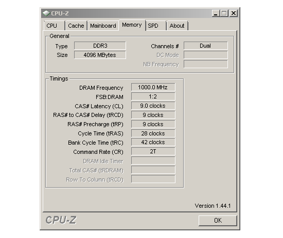
We were surprised to see the 790i clocked 4GB of DDR3 to 2000MHz without much hassle. However, performance at this frequency was lacking, as the system seemed to perform more like DDR2-1000 at 5-5-5-12 timings than DDR3-2000. For overall performance, we found FSB clocks just south of 475MHz FSB proved best.
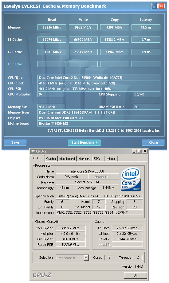
Memory at DDR3-1864 and a 45nm dual-core E8500 at about 4.2GHz (466x9) is a speedy combination. This is just about the spot where X48 with DDR3 begins to shine. It seems as though NVIDIA has been able to match Intel despite being several months late to the DDR3 party. You could argue the validity of that assessment of course; with the current price of DDR3 modules there's certainly no parties going on that we know of.
Will NVIDIA's 3-way SLI Make us Stand Up and Beg for More?
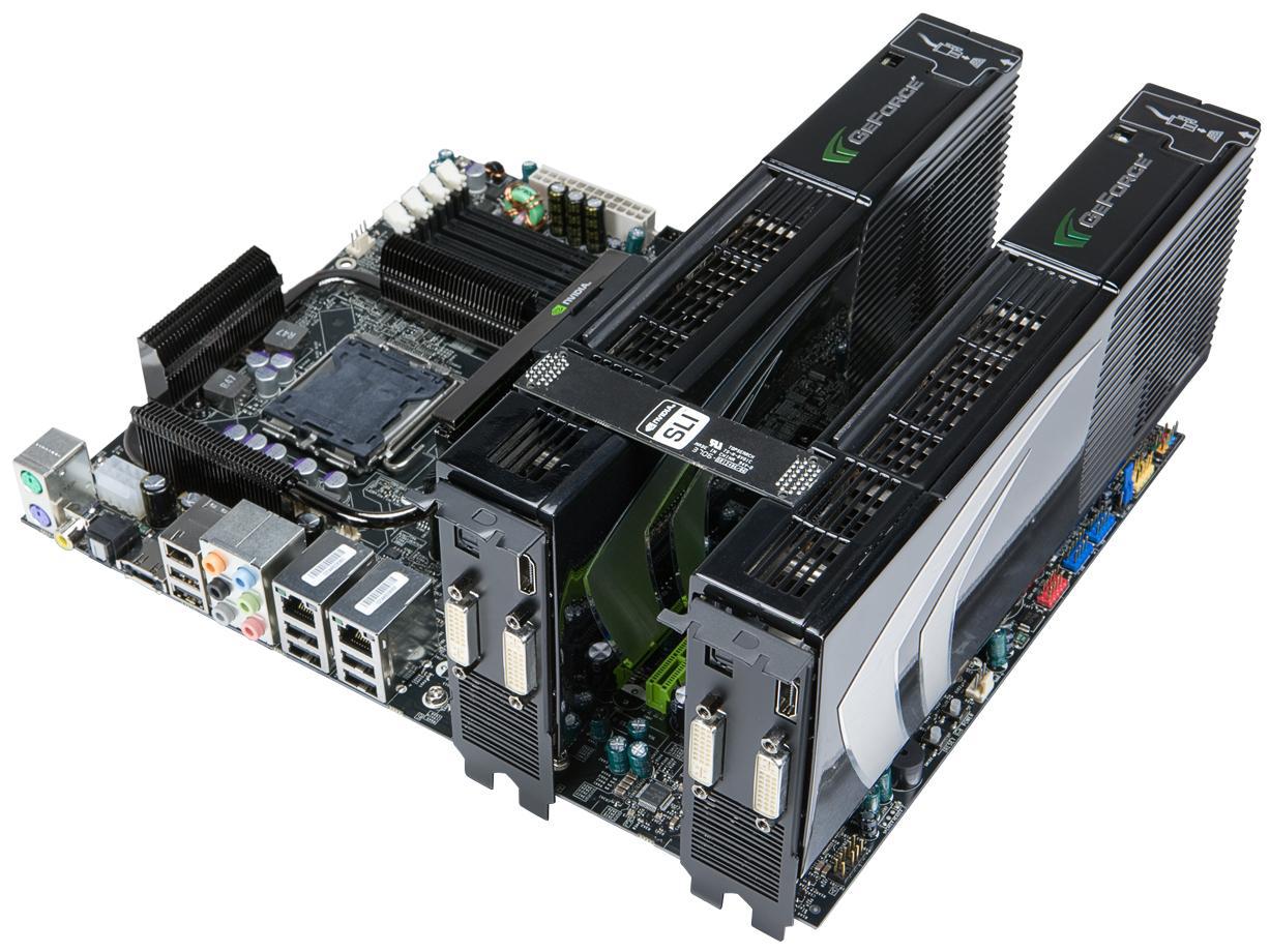
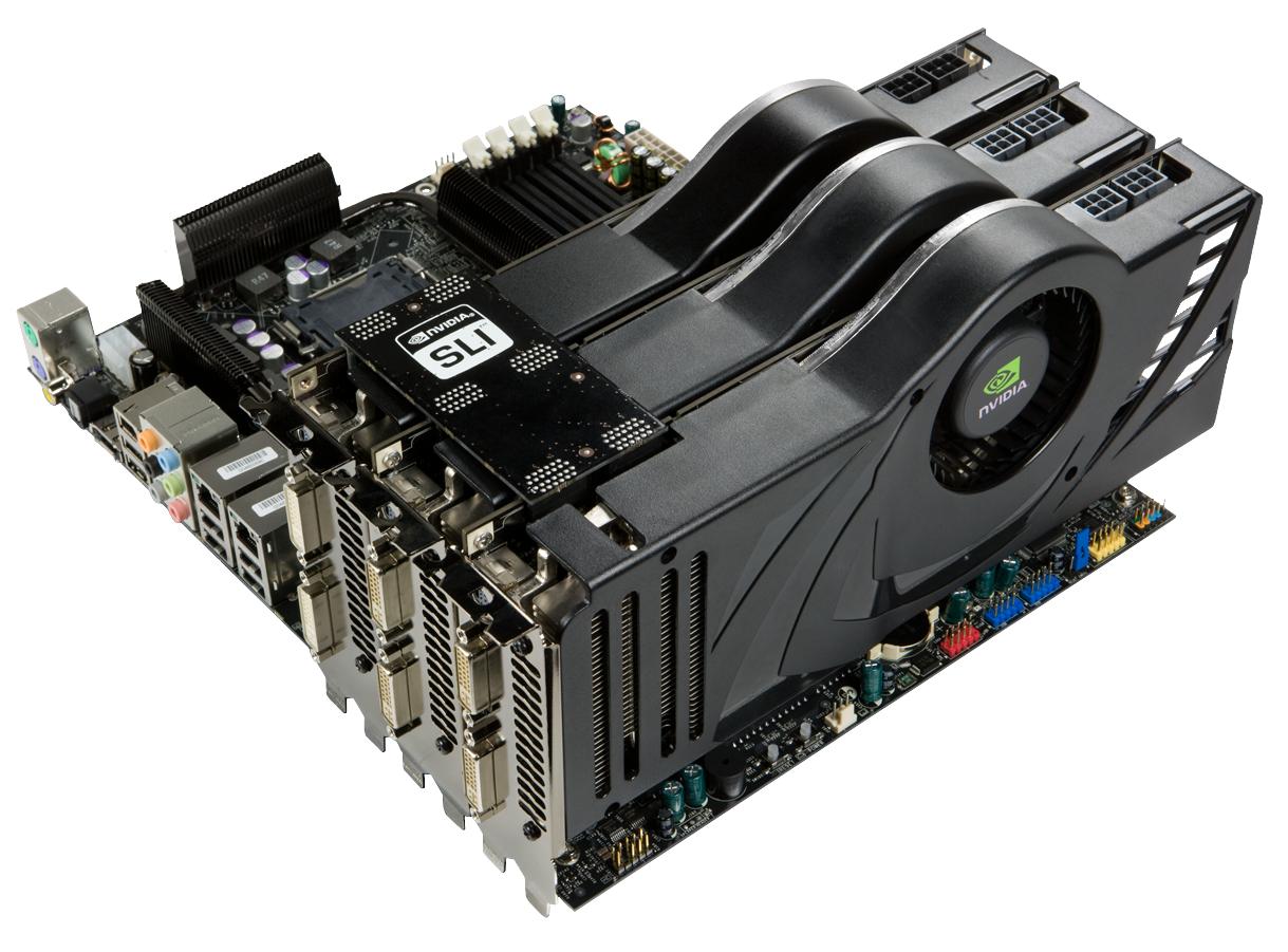 Fitting three NVIDIA GeForce 8800 Ultras in an nForce 790i board is quite easy. That is until your better half sees the next month's credit card statement. |
As of today, the ability to team more than two NVIDIA graphics cards for accelerated, parallel 3D game rendering requires some very specific hardware - namely no fewer than three GeForce 8800GTX or GeForce 8800 Ultra cards and either a 680i-, 780i- or 790i-based motherboard with the appropriate number of mechanical x16 PCIe expansion slots. System chassis and power supply requirements are no small potatoes either. A big case with plenty of cooling is a must and 1000W (or larger) PSUs become the standard when you decide to move up to play in these leagues. GPU overclocking takes on a completely new twist when you starting playing with this sort of power.
We decided to get a little creative and built a 790i-based system that included water-cooling on both the CPU and all three MSI 8800GTX cards. Full-coverage GPU blocks from EK Waterblocks were our components of choice, and going with 3/8" ID Tygon tubing meant we could use the shorter "stubby" barbs we would need if we wanted to have any hope of fitting things together so closely. In the end, our loop contained one D-tek FuZion CPU waterblock, three EK full-coverage GPU waterblocks, a single 2x120mm radiator from Cooler Master, a combination reservoir/pump also from Cooler Master, two inline thermal sensors, and about three feet of 3/8" ID and 5/8" OD clear tubing.
Yes, please.
Sure, our temperatures are not going to end up being that great, but we fit everything in a single case quite nicely and we only needed two medium-speed fans to cool the radiator and nothing else. At least our hearing would be safe. Check the sections on real-world gaming results to see how these cards stacked up against single and SLI GeForce 8800GTS 512MB (G92) configurations.
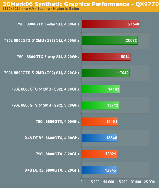
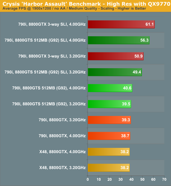
NVIDIA's 790i platform just barely manages to edge out Intel's X48 when it comes to single-card 8800GTX general graphics performance. Of course, this may have more to do with the slight advantage 790i has with the use of DDR3 over the DDR2 in the X48 board than anything else. Not surprisingly, the 8800GTS 512MB (G92) cards overtake the older 8800GTX cards quite easily. Keep in mind that we ran all of the GPUs at their stock speeds, as advertised by NVIDIA on their official company website. This removes any chance for performance variation due to different vendor's default clocks and allows us to test the cards as NVIDIA originally intended for them to be run.
NVIDIA's 3-way SLI shows only minor gains over a similarly configured 8800GTS (G92) SLI system - at 3.2GHz on our Intel QX9770 we only managed to outrun the pair of G92s by about 500 3DMarks. While the G92-based cards may have a core, shader, and memory clock advantage, the 3-way setup starts to pull away a little more as we ramp our quad-core CPU all the way to 4.0GHz. This suggests that the tri-SLI setup is starved for additional processing power, and more advanced architectures and higher computing speeds will be needed if we are ever going to experience the true potential this technology.
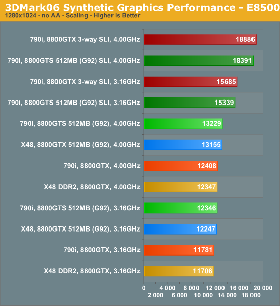
Gains with 3-way SLI were smaller with our E8500; multithreaded driver optimizations may play a role in this. Since we know the 790i is quite capable of fully utilizing a 45nm or 65nm quad-core CPU, picking one up is any easy choice if you've got the cash and are looking for maximum performance.
NVIDIA's Quad-SLI Graphics Makes a Comeback
 The NVIDIA GeForce 9800 GX2 cards certainly do look mean sitting side-by-side. We'll find out soon enough if they've got any bite to them… |
Quad-SLI, which made its first appearance with the introduction of the dual-GPU GeForce 7900 GX2, will make a return in the form of NVIDIA's highly anticipated GeForce 9800 GX2 card, currently scheduled for availability in late March to early April of this year. The 9800 GX2 will be based on the same G92 GPU used by 8800GTS 512MB cards, but with a slight twist from how single card SLI setups have been offered in the past. An onboard PCIe-to-PCIe bridge controller will split the incoming single x16 PCIe 2.0 lane into a pair of x16 PCIe 1.1a lanes. This creates additional latency for each incoming data packet as the controller will be responsible for correctly routing all traffic to the appropriate GPU, but it remains to be seen whether this makes an appreciable difference in performance or not.
We have also received word that the PCIe bridge chip will be able to arbitrate GPU-to-GPU traffic using the same PWShort and Broadcast functionality now natively present in the 790i SPP. This will be accomplished using an onboard nForce 200 chip, the same one previously paired with 780i. The "stop gap" solution of adding an extra bridge chip to 780i in order to provide PCI Express 2.0 compatibility now makes sense - it was only good business to include it at the time knowing it would find its rightful home months later with 9800 GX2. This time though the chip is bridging a single PCIe 2.0 x16 lane to two PCIe 1.1a lanes and not the other way around. It seems the chip is much more flexible than we might have previously imagined.
You will need either a 780i or 790i (Ultra) board in order to run Quad-SLI from NVIDIA as a minimum of two, full PCIe 2.0 x16 lanes will be required in order to properly host a pair of GeForce 9800 GX2 cards. Our NVIDIA GeForce 9800 GX2 review provides more information on these new video cards.
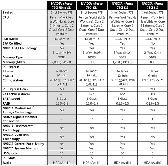
Synthetic DDR3 Memory Read, Write, and Copy Performance
Our testing was completed linked 'n' synced - that is, our DDR3 memory was run at a 2:1 ratio with the FSB as this consistently provided the best results and made 790i highly competitive with Intel X48 chipset, pulling way ahead when clocked to DDR3-2000 speeds; something that can be done nearly automatically thanks to EPP 2.0 profiles with SLI-ready memory modules.
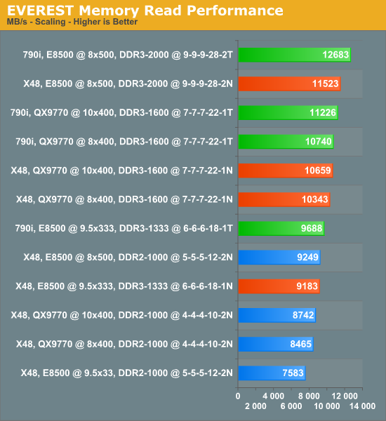
Read memory speeds aren't everything though - a delicate balance must be maintained between read and write performance if a chipset is going to be a winner. Again, we see 790i slightly outpacing X48, once more at 500MHz FSB. Other than that, we see 790i just about matching X48 head-to-head when it comes to memory write bandwidths. This is to be expected though as write performance is all about achieving maximum FSB. The problem with this is that some chipsets can leave a lot of read performance on the table if you tune solely for write speeds.
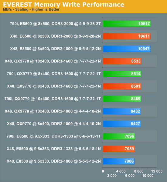
Memory copy benchmarks are unique in that they provide a great indication of just how well a memory controller balances the importance of read versus write performance. A chipset certainly cannot facilitate good copy speeds if either reads or writes are low. The memory controller must first read the data from memory before it can write it back to memory (this is the basis of a copy operation) and a bottleneck with either brings everything to a crawl. From this chart, we can conclude that Intel's X48 chipset is somewhat better than 790i when it comes to prioritizing these requests. So much so in fact that 500MHz FSB with an E8500 on X48 appears to outclass 790i by a healthy 6%.
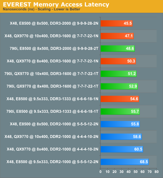
Low memory access latency and high memory read bandwidths go hand-in-hand. Low latencies are important because they characterize just how well the memory controller handles random memory access requests - that is, sequential read requests that cross memory bank boundaries and/or are not necessary in the same physical column as the prior read. For this reason, tests that stress a memory controller's ability to access memory in a highly random manner are especially dependant on access latencies. Even though 790i far exceeds X48 in sequential read performance, according to our results X48 may have a slight advantage when the requests become more randomized.
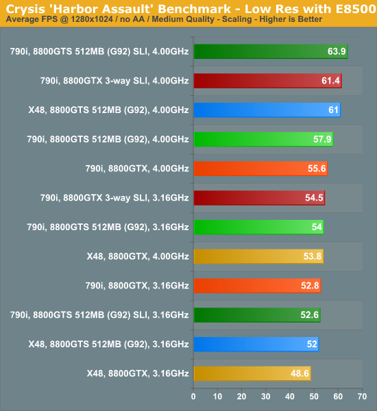
Real-World Gaming Results: Crysis
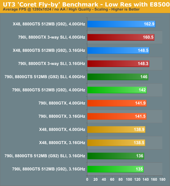
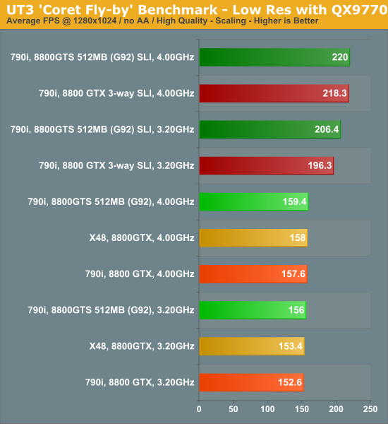
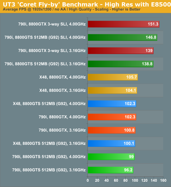
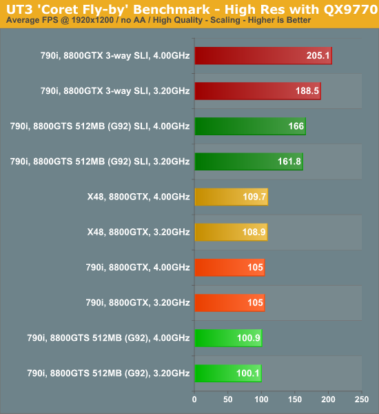
Real-World Gaming Results: Unreal Tournament 3
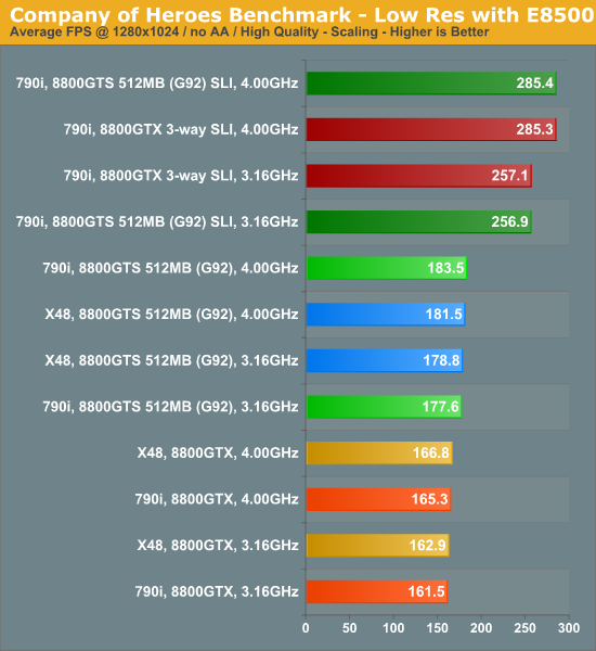
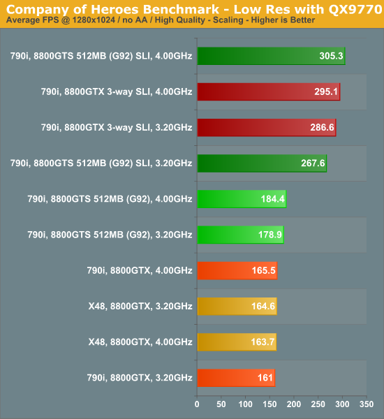
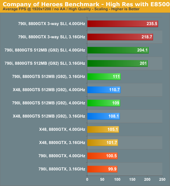
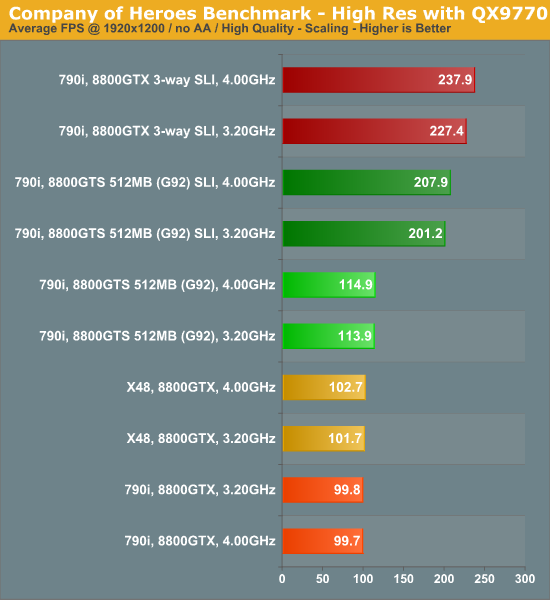
Real-World Gaming Results: Company of Heroes
First Thoughts
Our experience with 790i thus far has been overwhelmingly positive. It's clear to us that NVIDIA's decision to take the extra time needed to fully prepare the board and BIOS for retail release will end up paying dividends in the end. Many of the problems we experienced with early 780i boards are thankfully missing. The effort placed in providing good Auto values for overclocking has also been extremely helpful. Gamers that are looking to buy a system that is capable of practically overclocking itself should seriously consider the nForce 790i.
Without a doubt, one of the best reasons for buying any NVIDIA-based motherboard is and continues to be the support for SLI graphics configurations. Today's 8800GTS 512MB (G92) prices are low enough to make SLI-enabled gaming systems appear (Ed: almost) mainstream. A quick price check at many major online retailers shows such cards for as little as $249 each - and sometimes significantly less with a mail-in rebate. It was not long ago that the very mention of the price of an SLI system would make your wallet cower in fear; G92 has definitely changed that for the better. NVIDIA tells us they are committed to providing sufficient product at launch, so expect to see 790i hit the shelves almost immediately. For those that are moving up from 680i/780i, don't forget to buy some DDR3. After that, it's an almost seamless transplant moving system components over from one board to the other.
One thing we were happy to see was the improved memory performance at higher frequencies made possible by NVIDIA's latest BIOS. We were experiencing dismal read and copy speeds when using any FSB in excess of 475 FSB. NVIDIA BIOS engineers quickly went to work following a discussion we had detailing our findings and within two days we had our response. The fix provided the performance we initial expected to come from DDR3-2000 memory speeds and the new benchmark results showed the 790i to be devilishly fast afterall. This makes the E8400 with a 9x multiplier a rather good choice when it comes to selecting a CPU. Five-hundread megaHertz and a 9x multi yields a final CPU speed of just under 4.5GHz (or you can go 500x8.5 for an easy 4.25GHz) - a great place to be when it comes to maximizing the hidden potential of any 45nm dual-core microprocessor. If anything, this should be another testament to the importance of selecting a CPU with a higher multiplier. True, while the more modestly price E8200 can certainly be tempting (assuming you can find a seller willing to give you a fair price), you will most likely end up kicking yourself for not going with the E8400 or something with a higher multiplier.
We try to keep in close contact with all of the major vendors, NVIDIA included. You can be certain we will continue to do whatever we can to help improve 790i and future platforms. The nForce 790i SPP is already light years ahead of 780i - 45nm CPU overclocking support is significantly improved and DDR3 memory speeds up around 2.0GHz are wicked fast. DDR3 memory should continue to gain in popularity as prices continue to drop and DDR2 begins to make an exit from the market. Some of the better modules are really starting to shine; the Crucial Ballistix we were offered for review were able to reach speeds in excess of 2.0GHz with no more than 1.9V on the 790i.
You may also want to keep a lookout for the introduction of a few new ESA-enabled components over the coming weeks. We have just received word that OCZ plans to offer a 1000W PSU with ESA-provided real-time current, voltage, and efficiency monitoring. Knowing your PSU is operating well within rated specifications is one less thing to worry about when pushing your system to the limits.
This is first enthusiast level chipset from NVIDIA for the Intel platform that we refuse to refer to as a duck in the labs. You see, just like a duck, the 680i/780i based motherboards seem to wake up in a different world every day. All indications at this point are that NVIDIA finally got their act completely together with the 790i. True, it might not have the same heritage as the Intel X48, but NVIDIA has finally put together a compelling platform that we would not hesitate to use as our main system without the condition of "gaming" being its primary purpose in life.
While this platform will surely satisfy most enthusiasts with its enticing performance, there is one caveat that will relegate it to a select few users. Pricing on these boards is expected to be in the $350 to $400 range. Combine that with the cost of 4GB of DDR3-1800+ memory and you can see why most people will cower at the thought of an upgrade at this time. In the end, it simply comes down to a decision as to whether you want the overall fastest platform available for Intel's latest processor series or you like to eat on a regular basis. Some of us could stand to lose a few pounds….


