Original Link: https://www.anandtech.com/show/2404
Overclocking Intel's New 45nm QX9650: The Rules Have Changed
by Kris Boughton on December 19, 2007 2:00 AM EST- Posted in
- CPUs
Introduction
Intel has once again re-energized the overclocking community with the recent release of the Core 2 Extreme QX9650 quad-core processor, the first of many new mobile, desktop, and server CPUs fabricated using their radically new 45nm process technology. Early results have highlighted Intel's extremely conservative approach in assigning processor power specifications and because of this, users looking to push their systems beyond rated speeds are finding they have a lot more headroom than normally expected. Our overclocking trials have met with great success, as exploiting this processor's hidden performance margin is easier than ever imagined.
The last seven generations of Intel processors have utilized traditional metal oxide semiconductor (MOS) materials, namely silicon dioxide (SiO2) and other polysilicates. This has spanned a period starting with the Pentium, originally built on 0.6 micron (600nm) node technology, all the way to Core 2 Duo/Quad parts built on 65nm. However, for the first time in over 40 years, Intel has significantly changed some of the basic components used in transistor fabrication. Hafnium dioxide (HfO2) has replaced SiO2 as the gate dielectric material, along with other carefully chosen new metals, for use in the formation of gate electrodes in both PMOS and NMOS transistors. These new materials, along with the right process recipe, have cut gate leakage by a factor of more than 10x while simultaneously delivering an astonishing 30% decrease in transistor switching energy. The result is a cooler running, more energy efficient, and high-performance processing powerhouse.
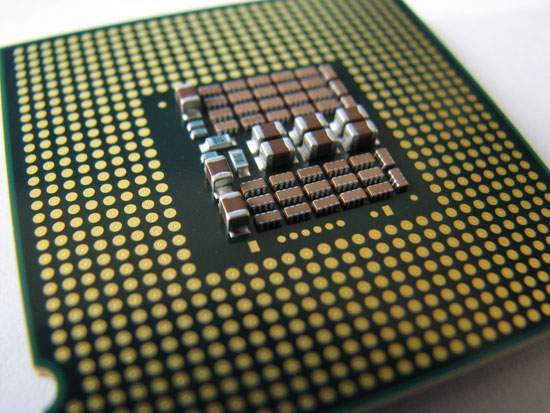
Intel's Core 2 Extreme QX9650 in the classic LGA775 package
Moving to a smaller node process technology allows for the potential of two things to happen. The first is the ability to make smaller production dies, reducing manufacturing costs, and ultimately making products more affordable to the consumer. Alternatively, designers can take advantage of the increased transistor density made possible by the new process and develop next-generation solutions that pack even more transistors into the same space as before. Smaller transistors also allow Intel to take advantage of lower switching energies up to a limit. This is true until smaller and smaller transistor gate dielectric boundary layers create conditions in which power leakage - even with the transistors in the "off" state - become excessive. From this point on something will have to change if Moore's "Law" is going to continue.
With much fanfare, Intel released the highly anticipated Core 2 Extreme QX9650 Processor just a few shorts weeks ago, knowing that the high price would be little more than a speed bump for high-performance enthusiasts. More practical-minded users will have to wait until early 2008 before experiencing the mainstream release. Naturally, we wasted no time in bringing you this first-hand look at the QX9650's expansive overclocking potential. Although our experience has not been entirely without problems - we will cover the good and bad later in more detail - we must commend Intel on the development of another great product. Without a doubt, the QX9650 has taken its rightful place in the winner's circle.
Our maximum overclock on water is nothing short of impressive
Until now, achieving this level of overclock with water-cooling alone was unheard of and we find ourselves feeling punch drunk with the speed. Indeed, finding applications that make practical use of this ridiculous amount of processing power is exceedingly difficult - few programs these days efficiently utilize two cores, let alone four. Obviously, scenarios that make intelligent use of the QX9650's exceptional parallel processing capabilities stand to benefit the most. Good examples are video (and to a lesser extent audio) editing, rendering, ray tracing, 3D modeling, DivX/Xvid encoding operations, and of course gaming (when properly coded and without GPU limitations).
We hope our in-depth look at QX9650 overclocking will provide new information even for those who have been into the overclocking scene for some time. Others, looking for the right opportunity to try their hand at voiding their processor's warranty, should find just about everything they need get started down the long path towards an overclocking addiction. Strap on your heatsinks, tweak your voltages, and join us as we see exactly what Penryn and 45nm brings to the overclocking party.
Will the Real QX9650 Power Consumption Please Stand Up?
The recent attention highlighting the conflicting manners in which Intel and AMD quote processor power consumption figures has generated a fair amount of discussion regarding which methodology more closely represents the truth. In reality, we can see the merits of both systems, and which one is more valuable to the consumer is largely a matter of personal perception.
To this day Intel still provides processor TDP (thermal design power) specifications with a single purpose in mind - ensuring thermal engineers have the information they need to do their jobs. Intel knows companies providing platforms based on their products must be able to design and manufacture cooling solutions capable of dissipating the installed processor's maximum heat production - all without violating temperature limits. Designing around these worst-case values ensures the system remains stable under all computing conditions.
AMD's focus is very different, as they have decided to use this data as a marketing tool. By drawing attention to the processor APC (average power consumption), they hope to appeal to businesses looking to lower costs associated with their data infrastructure's operation. Although most end users find little reason to concern themselves with the relatively small monthly savings that can come from a single system's lowered power consumption, this can be a significant sum of money for corporations supporting hundreds or even thousands of workstations. Then again, any business supporting thousands of computers usually has other concerns. Do they worry more about the $5,000-$10,000 per month (or more) spent on the employee using a workstation, or the $10-$30 spent on the power for the workstation? The greater concern is often whether or not a given location has the capacity to power the workstations, not how much the power will cost.
With that said, we would argue that AMD is pandering to the public while Intel has chosen to support the industry developers. We can all certainly agree though: no matter which method you believe is more correct, quoted numbers are useless without a consistent means for calculation.
Surprisingly, Intel has chosen to leave the QX9650's TDP unchanged from the 65nm QX6850's given value of 130W. This is a little confusing as reports from Intel on 45nm process technology improvements provide us with claims of switching energy efficiency increases of up to 30% and a reduction in transistor gate leakages of 10x or more. Could basic core performance improvements such as the incorporation of the new SSE4 instruction set have made such a difference in overall CPU efficiency? We think not. Obviously, there is something more going on here; either the QX6850 TDP is vastly under-rated or the QX9650 is much better than suggested. Perhaps over-rating the QX9650's TDP gives Intel the option in claiming further thermal improvements later. We will share the method we used in calculating a more representative TDP rating for our 45nm quad-core in a moment, but we found the value to be closer to 100W - some 30W less than the figure provided by the blue team, and right in line with the 30% energy efficiency increase.
Determining just how much power a particular processor consumes at a given operating frequency is more difficult than one might originally think. A few different methods exist for estimating these values - one requires nothing more that the processor's specified TDP and then scales this value based on a given overclocked core frequency and voltage. This isn't going to cut it for us, especially considering this technique insists we place full faith in Intel's quoted QX9650 TDP, a number we know to be sometimes unrepresentative of actual operating conditions. Instead, we decided to get creative and develop our own method. The concept is rather simple: we will measure the power draw from the wall, subtract off power consumption for "static" components, correct for PSU efficiency, and then devise a means for determining what portion of the remaining power the CPU consumes - by somehow attributing the remainder to "everything else." The biggest challenge will be devising a means for accurately determining where to place this final split.
Choosing the right PSU is vital in the success of our mission, and employing the services of a Corsair unit means we can take advantage of the published efficiency curves. Monitoring and recording total system power draw is easy thanks to our Kill-A-Watt from P3 International. Finally, calculating just how much power is used by static loads (fans, pumps, HDDs, etc.) won't be too hard at all - simply noting the power draw before and after disconnecting the load is quick and effective. Indeed, developing a method for subtracting off power consumed by the motherboard, memory, and graphics card is going to require the most thought.
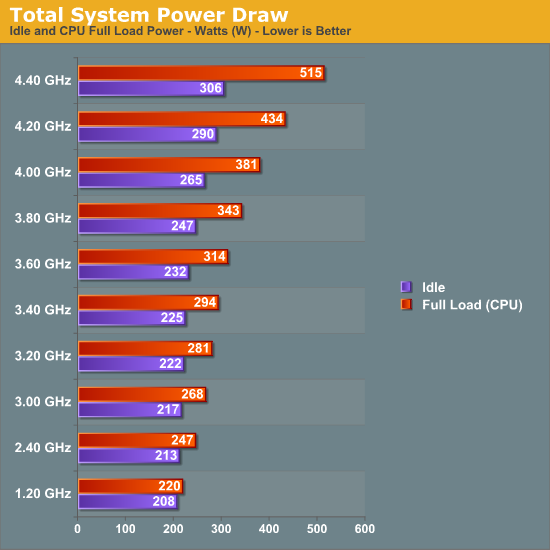
Our approach is rather unique: we vary CPU frequency and voltage and then plot the base system load delta versus frequency. System load delta is the difference between wall power minus static loads at CPU full load and wall power minus static loads at idle - both corrected for PSU efficiency. Graphing the delta means that the plotted power varies solely as a function of CPU speed. Our immediate results generate the following graph.
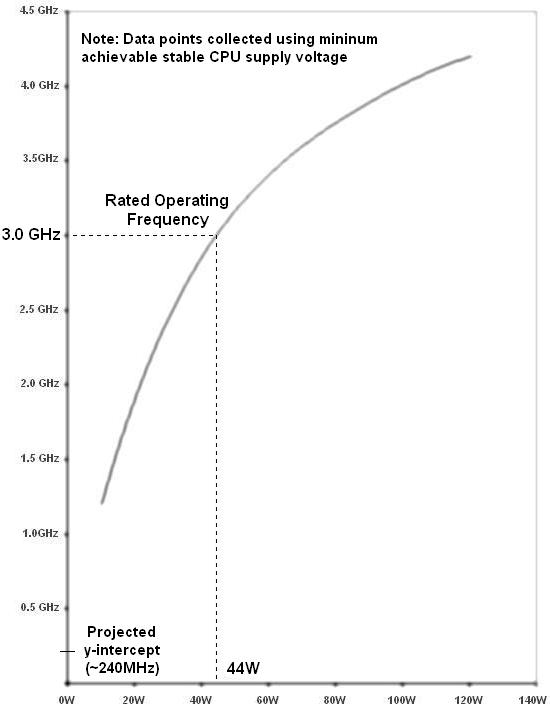
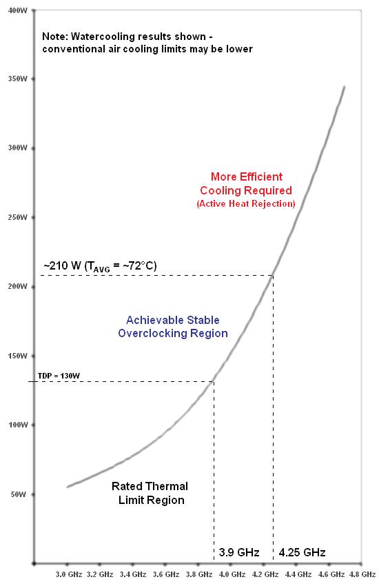
Base System Power Delta (W) versus Processor Frequency (GHz)
Extending the curve downwards allows us to extrapolate our plot's predicted y-intercept. Mathematically, this point represents the frequency in which CPU full load power minus idle power is zero (CPU idle power equals CPU full power). Logic suggests that as the CPU full load power approaches zero so will idle power, especially considering idle power should always be less than the full load power. Without much argument, we find ourselves accepting this as our CPU minimum energy frequency (about 240MHz).
We then plot the base system idle power (wall power minus static loads at idle, again corrected for PSU efficiency) versus the same set of frequencies. Creating a best-fit equation and solving for power using the minimum energy frequency found in the previous graph above gives us the base system power consumption with the CPU at its minimum energy (near zero). This is as close we are going to come to quantitatively determining the idle power consumption of the motherboard, memory, and graphics card combined. We calculated a value of 110W using an ASUS P5E3, 4GB of OCZ DDR3, and a single 8800 Ultra resting comfortably at 500Mhz on a 2D desktop. More likely than not the power-hungry GPU and overclocked X38 chipset make up the lion's share of this value.
With this number our goal is in sight - subtracting this value from the corrected base system idle values used in the creation of our second graph (not shown) gives us the CPU idle power points. Adding to these the base system load deltas plotted in the figure above provides us with the final unknowns - actual CPU full load power values. Joining these two sets of data points gives us the data below.
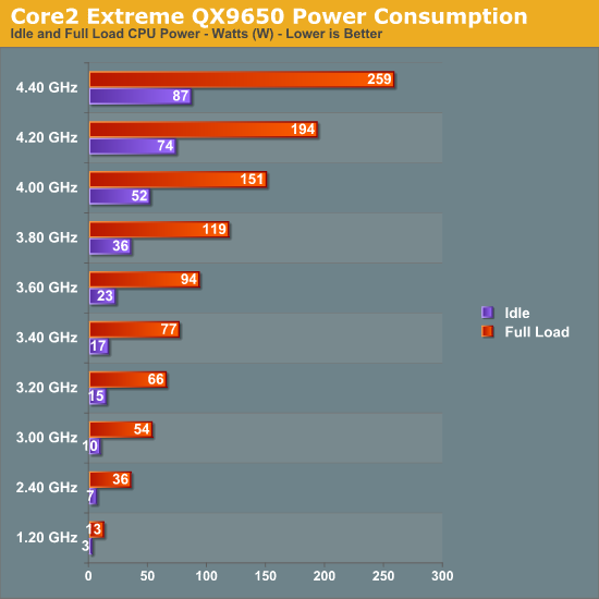
This graph rewards our hard work by providing us with a wealth of knowledge. Although the values above are highly precise only when referring to our particular QX9650 (every CPU is a little different), the accuracy of our method should be very good. The first thing we notice is how full load power consumption quickly increases to almost uncontrollable levels when pushing above ~4.25GHz. In fact, we found achieving true stability any higher nearly impossible with water-cooling alone. Users who are familiar with overclocking will recognize this trend: a CPU usually scales extremely well up to a certain point, beyond which any further overclocking requires an excessive amount of additional voltage. This is normal and exactly where this point lies is a function of cooling and silicon limits (i.e. process technology) and in reality has very little to do with luck.
An example of the findings that can be developed by measuring system response
We made this last graph using our CPU full load power consumption/frequency pair data points from the figure above. Based on our examinations, just about every Core 2 Extreme QX9650 owner should have little trouble accomplishing at least a 3.9GHz overclock. Upgrading the cooling used will at best provide modest improvements as these quad-cores begin to generate a lot of heat when pushed much further.
Exploring the Limits of 45nm Silicon
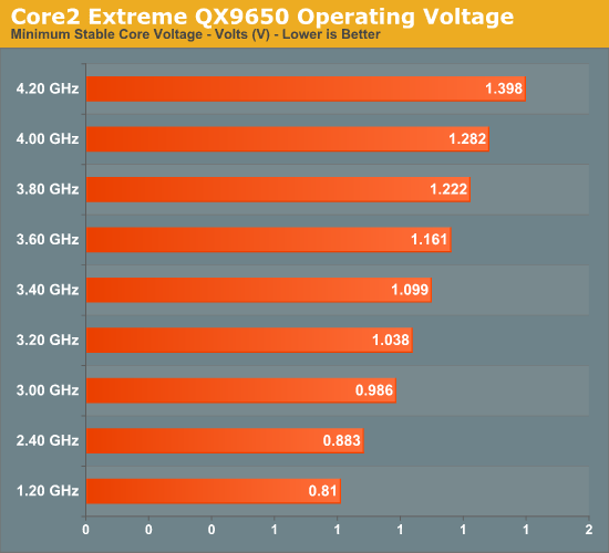
During the course of our testing we made a rather interesting discovery regarding 45nm silicon scaling: a window exists in which CPU frequency responds in a highly proportional manner. Calculating this value later tells us that between 3.0GHz and 4.0GHz our processor requires ~0.3mV (0.0003V) more Vcore for each one megahertz increase in core frequency. Since our QX9650 is capable of running the stock 3.0GHz setting at only 0.98V, this means that achieving a stable 3.6GHz overclock requires 0.98V + (0.3mV/MHz)(600MHz) = 1.16V. This general trend continues all the way to about 4.0GHz where we found total stability at an amazingly low 1.28V. We cannot help but feel excited about Intel's new 45nm process, especially considering such early maturity.
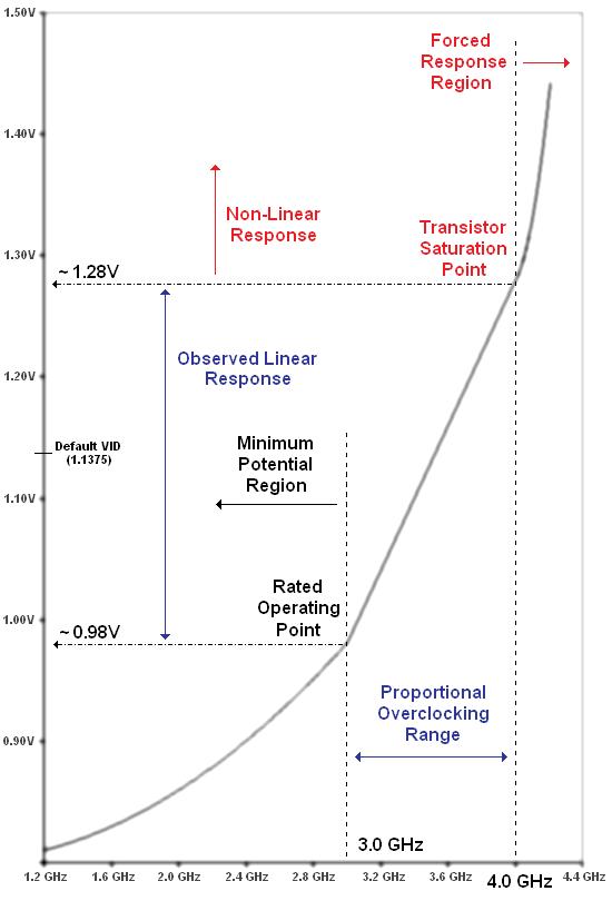
Always target the higher end of the Proportional Overclocking Region
Dropping below 3.0GHz allows us a chance to experiment in the world of low-voltage (LV) and ultra low-voltage (ULV) clocking. Two point four gigahertz (2.4GHz) was possible at only 0.90V. Additionally, the lowest possible core speed that we could dial-in using the ASUS P5E3 (6 x 200MHz = 1.20GHz) had no problems maintaining stability at only 0.81V. It's interesting to note that this is also the lowest Vcore we could supply the CPU, as VID settings below 0.85000 were not available for use. As an aside, the VRM 11.0 specification, used extensively by motherboards supporting 65nm CPUs, calls for selection values down to 0.70000V.
As expected, pushing the QX9650 above 4.0GHz, although possible, also demands more Vcore than predicted by our simple scaling equation. In fact, running well in excess of this speed requires a nearly exponential increase in voltage. At this point gains are small and generally not worth the extra heat produced because of the excess power consumed. Clearly, the more efficient silicon switching that comes with better cooling is needed if we planning to go much higher. Oddly enough, for the first time in water-cooled quad-core history, we feel as though heat is not the limiting factor. Rather than push this finding aside, we decided to examine the cause a little more closely.

We start our investigation by comparing our measured processor power consumption values with those found through use of the well-known power scaling equation (shown above). The equation wonderfully predicts what we see at lower frequencies but quickly falls behind actual measured values when looking at higher speeds:
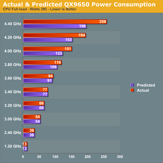
A quick check for clues as to the differences turns up one important oversight. Intel's newest power prediction equation includes an extra factor - processor capacitance. Research indicates that the capacitance associated with the transistors gates has become quite significant; possibly more so with 45nm Hi-k transistors than those made using any other previous process technology. We decided to establish the region boundary in the plot above using the point in which this effect became significant, even though the extra transistor capacitance created at higher switching frequencies begins to manifest itself as additional power required at lower processor speeds (around 3.6GHz). At 4.0GHz this additional factor accounts for 25% more power than would otherwise be predicted.
Although we cannot explain exactly why capacitance becomes such a large factor at higher speeds, average core temperature may be a factor. This would certainly help to explain why microprocessors experience such dramatic increases in switching efficiencies when super cooled. Typically, a processor needs significantly less voltage in order to run equivalent speeds under phase-change or liquid nitrogen than would be required with typical air or water-cooling. In fact, based on what we have seen, these 45nm processors may be the first of many in which overclockers find they reach silicon limits before anything else. In the past, it was comforting to know that a bigger heatsink, more powerful fan, or a better water block held the promise of a higher overclock; with 45nm this may no longer be the case.
An Unexpected Loss of Performance at Higher Speeds
It looks as though Core 1 is having trouble keeping up with the other three
We first suspected our motherboard's VRM circuitry might have been overheating while supplying the high load current. If this were the case the PWM IC would communicate with the processor using the PROCHOT pad and the CPU would respond by modulating an internal clocking signal to each core thereby artificially lowering the load and allowing the VRM to cool - a failsafe meant to save the VRM should things start to get too hot. Eventually our frustration in the matter led us to modify our board by disconnecting the control signal altogether. Unfortunately, there was no change.
We discussed the possibility of having discovered an undocumented erratum, thinking that maybe some internal control logic was at fault. The Analog Devices ADP3228 PWM controller used on the ASUS P5E3 motherboard, designed in compliance with Intel's new VRM 11.1 specification, includes a new power management feature intended to improve power circuit efficiency during periods of light loading. When directed by the CPU the VRM essentially disables four of the eight power delivery phases until they are later command back on. (This is not unlike the concept put to use in the automobile industry wherein half an internal combustion engine shuts down while cruising in order to improve fuel economy.) However, we are unable to completely rule out a possible incompatibility as no one is aware of how to go about disabling this feature.
In fact, we believe what we are seeing may be nothing more than a CPU protection mechanism in action. The Core 2 family of processors is extremely resilient to abuse - reports of failures due to overvoltage or over current incidents are exceedingly rare. Features such as these work by clamping processor input voltage (and current) to tolerable levels in order to prevent permanent damage. Further testing reveals we have some level of control with regards to the "throttling" - it seems that by slightly lowering the VID, and thus in turn the CPU supply voltage, we are able to complete testing at some of the same frequencies with no noticeable performance degradation issues. Could it be possible that we found a processor protection limit with nothing more than common water-cooling? Normally, such discoveries are the domain of those that freeze their CPUs with one or more rotary compressors or copious amounts of liquid nitrogen. Given the enormous power increases observed at these higher speeds due to what might be a processor capacitance effect, we cannot help but wonder if these new limitations are an unintended consequence of Intel's 45nm process.
If what we believe is true the implications could be enormous. The need for certain industries built on delivering high-performance cooling solutions to the overclocking community would be largely invalidated. What's the point in spending more money on a more effective heatsink if there's nothing to gain? With that said, we honestly believe a new direction in CPU overclocking may soon be upon us. While there will always be those that continue to push processors to their absolute limits, the majority of us will find our new "performance" benchmark in efficiency. This makes sense though - the market has been heading this way for years now and overclockers may have simply chosen to ignore the obvious. The multi-core era we now live in places a heavy emphasis on performance-per-watt figures and other measurable efficiencies. Does anyone else find it odd that Intel's flagship product, the QX9650, comes at exactly the same speed bin as the previous 65nm offering? All this talk of improved performance and efficiency and not even a measly frequency bump - perhaps Intel is trying to tell us something.
Intel Processor Power Delivery Guidelines
If you've ever overclocked a system, chances are that at some point or another you've had opportunity to become upset with your Vdroop "problem." Some users, confused as to why their system refuses to exactly match actual processor supply voltage to the value specified in BIOS, are quick to blame the quality their motherboard; still others find fault with the difference noted between their board's idle and full-load processor supply voltages. Actually, load line droop (Vdroop) is an inherent part of any Intel power delivery design specification and serves an important role in maintaining system stability. In most cases, comments regarding unacceptable power delivery performance are completely unfounded. To make matters worse, unjustified negative consumer perception surrounding this often misunderstood design feature eventually forced a few motherboard manufacturers to respond to enthusiasts' demands for action by adding an option in their BIOS that effectively disables this important function.
Based on the currently running tasks, processor load can vary significantly during system operation. The voltage regulator module (VRM) circuit closely regulates CPU supply voltage by sensing instantaneous changes in processor loading and then responds by varying the individual on-time for a bank of power MOSFETs used to charge a multi-phased LC network. This LC network is responsible for providing all of the power demanded by the processor. If the VRM senses a decreasing supply voltage, it provides more current; the opposite is true in the case where voltage is rising. This cycle of sense-and-correct, known as negative feedback, can occur at that rate of thousands to millions of times per second, depending on the particular circuit's switching frequency.
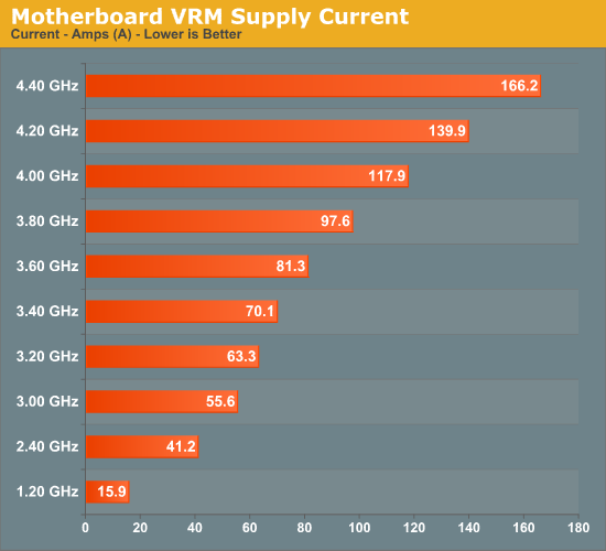
Just like CPU power, CPU supply current increases quickly at higher frequencies
During periods of high CPU demand, the VRM circuit works hard to supply the current required by the processor. However, as soon as that load is gone, the VRM circuit must act quickly in order to reduce the current supply to the level needed to match the new demand. Because it's impossible for the VRM circuit to respond instantaneously, the larger the load change the greater the maximum potential peak overshoot voltage. Controlling the magnitude of these peak values is critical for maintaining system stability. By positioning the processor's no-load (idle) voltage level higher during periods of light loading, it's possible to sustain a larger negative voltage dip without crossing the processor's lower specified voltage limit. In addition, "drooping" the load voltage as a function of supply current allows the VRM to effectively limit the maximum positive peak overshoot voltage (experienced during a heavy to light load transient) to a value below the maximum allowable CPU voltage. This resulting control system ensures the processor supply voltage, regardless of CPU load, never violates a specified limit. The following figure should help to illustrate these concepts.
As intended, Voffset and Vdroop ensure that the supply voltage never exceeds CPU VID
The CPU VID setting establishes the absolute maximum allowable processor supply voltage experienced during transient conditions and is not the target idle voltage. We hope this statement draws attention to this important distinction, as many believe the opposite to be true - a mistake all too commonly made. Together, Vdroop and Voffset ensure that the peak CPU supply voltage seen during heavy to light loading changes remains well below the established maximum. If you determine that 1.17V, as in the case above, is not sufficient for maintaining CPU stability under load, simply increasing the CPU VID does correct the problem. Let's now examine how the system responds if we remove Voffset.
Voltage oscillations while leaving heavy load can cause problems with no Voffset
As we can see, the system exceeds maximum allowable processor voltage whenever any heavy to light load transient is significant enough to warrant one or more voltage excursions above the CPU VID value. Even worse, this all happens without the user's knowledge. Again, removing Voffset completely undermines the purpose of the VID setting - which establishes the maximum CPU voltage, not the target value.
Intel Processor Power Delivery Guidelines (Cont'd)
In this next case we eliminate Vdroop altogether and examine the chaos that ensues. As illustrated by our model, removing Vdroop does nothing to reduce the magnitude of the idle to full-load transient but does increase the settling time as the VRM must recover to a higher final regulation voltage. As in the case of no Voffset, it is possible to exceed the maximum allowable CPU voltage (VID). Clearly, removing Vdroop gains us nothing and only serves to create problems that are more serious.
No Vdroop means the VRM circuit must work harder at maintaining a constant voltage
So what happens when we remove both Voffset and Vdroop? The answer is simple - bad things. Although the difference between the maximum positive and negative peak overshoot are the same, severe violations to the CPU VID limit occur. If you're asking yourself what's the problem with this, consider the case of a CPU VID of 1.60000V - because the user feels this is the absolute maximum CPU voltage that they will allow. Just how high do you think CPU voltage will go after leaving a heavy load condition? We can't be sure without knowing more of the details, but we can certainly conclude that it will be well in excess of 1.6V. If you've ever run a benchmark only to have your system crash right as it finishes then you have experienced the consequences of this poor setup.
The user gives up all control over the CPU supply voltage with no Voffset or Vdroop
Finally, let's take one last real-world look at the consequences of removing Vdroop. ASUS' implementation of this feature, labeled as Load Line Calibration and included with their latest line of motherboards, is particularly worthy of our attention for a number of reasons. The first is that setting lower voltages with this option enabled actually results in a condition in which the CPU voltage under load is higher than the idle voltage. Imagine our confusion as we desperately struggle to understand why our system is Prime95 stable for days yet continues to crash under absolutely no load. What's more, in spite of the absence of droop and for reasons unknown, enabling this feature artificially raises our CPU's minimum stable core voltage at 4.0GHz from 1.28V to about 1.33V. As a result, our system uses more power under load than is otherwise necessary. Our efforts to reduce our processor's supply voltage backfired - instead of lowering the system's total power consumption we managed to affect a 20W increase.

Suffice it to say, we found it better to leave Load Line Calibration disabled
With Load Line Calibration disabled in BIOS, setting a CPU Voltage VID of 1.38750 resulted in a no-load voltage of about 1.34V and a full-load value of 1.28V. Enabling this feature and lowering the VID to 1.35000V produced a constant CPU supply voltage, regardless of load (or so it seemed), of 1.33V. Setting a lower VID resulted in a blue screen during Windows boot. Idle voltage was relatively unchanged at about 1.33-1.34V but the full-load voltage required increased by 50mV with no benefit. As you might guess, we recommend you leave this option disabled.
Hopefully we've shown you enough to understand exactly why Voffset and Vdroop are important. Please give second thought to your actions if you're in the habit of defeating these essential system safeguards.
Testing System Stability with Prime95
For over 10 years a site operated by a group called the Great Internet Mersenne Prime Search (GIMPS) has sponsored one of the oldest and longest-running distributed computer projects. A Mersenne prime is a prime of the form 2P-1 where "P" is a prime number (an integer greater than one is called a prime number if its only divisors are one and itself). At this time there are only 44 known Mersenne primes. The simple client program, called Prime95, originally released and made available for public download in early January 1996, allows users interested in participating in the search for other Mersenne primes the opportunity to donate spare CPU cycles to the cause. Although few overclockers participate in GIMPS, many use Prime95 for testing overall system stability. While there are other programs available for download designed specifically for this reason, few can match the ease of use and clean interface provided by Prime95.
The load placed on the processor is quite intense (nominally 100% on each core, as reported by Windows) and if there are any weaknesses in the system Prime95 will quickly find them and alert the user. Additionally, newer versions of the program automatically detect the system's processor core count and run the appropriate number of threads (one per core), ensuring maximum system load with the need for little to no user input. It is important to note that high system loads can stress the power supply unit (PSU), motherboard power circuit components, and other auxiliary power delivery systems. Ultimately, the user is accountable for observing responsible testing practices at all times.
Failures can range from simple rounding errors and system locks to the more serious complete system shutdown/reset. As with most testing the key to success comes in understanding what each different failure type means and how to adjust the incorrect setting(s) properly. Because Prime95 tests both the memory subsystem and processor simultaneously, it's not always clear which component is causing the error without first developing a proper testing methodology. Although you may be tempted to immediately begin hunting for your CPU's maximum stable frequency, it's better to save this for later. First efforts should focus on learning the limits of your particular motherboard's memory subsystem. Ignoring this recommendation can lead to situations in which a system's instability is attributed to errors in the wrong component (i.e., the CPU instead of the MCH or RAM).
To begin, we first start by identifying personal limits regarding measurable system parameters. By bounding the range of acceptable values, we protect ourselves from needless component damage - or even worse, complete failure. We have listed below the parameters we consider critical when overclocking any system. In most cases, monitoring and limiting these values will help to ensure trouble-free testing.
Overall System Power Consumption: This is the system's total power draw as measured from the wall. As such, this is the power usage sum of all components as well as power used by the PSU in converting household AC supply current to the DC rails used by the system. P3 International makes a wonderful and inexpensive product called the Kill-A-Watt that can monitor your system's instantaneous power draw (Watts), volts-amps (VA) input, PSU input voltage (V), PSU input current (A), and kW-hr power usage.
A conservative efficiency factor of about 80% works for most of today's high-quality PSUs - meaning that 20% of the total system power consumption goes to power conversion losses in the PSU alone. (Although absolute PSU efficiency is a function of load, we estimate this value here as a single rating for the sake of simplicity.) Knowing this we can estimate how much power the system is really using and how much is nothing more that heat dissipated by the power supply. For example, if your system draws 300W under load then 240W (0.8 x 300W) is the load on the output of the PSU and the remaining 60W (300W - 240W) leaves the PSU as heat. It is important to note that manufacturers rate PSUs based on their power delivery capabilities (output) and not their maximum input power.
Using what we have learned so far, we can calculate the maximum allowable wall power draw for any PSU. Consider the case of a high-quality 600W unit with a conservative efficiency rating of 80%. First find 90% of the maximum output rating (0.9 x 600W = 540W) - this allows us to limit ourselves to at least a small margin below our PSU's maximum load. Now divided that by 0.8: 540W / 0.8 = 675W. For a good 600W PSU we feel comfortable in limiting ourselves to a maximum sustained wall power draw of about 675W as read by our Kill-A-Watt. (Should you decide to use a lower quality power supply, you will get lower efficiency and you won't want to load the PSU as much. So, 70% efficiency and a maximum load of 75% of the rated 600W would yield 643W… only your components are getting far less actual power and the PSU needs to expel a lot more heat. That's why most overclockers value a good PSU.)
Our PSU's total power draw as a function of CPU speed (full load)
Keep in mind that the power consumption values based on CPU testing alone will not be representative of total system load when running graphics intensive loads, like 3D gaming. The GPU(s) also contribute significantly to this value. Be sure to account for this when establishing your upper power consumption limit. Alternatively, buy a more powerful PSU as overstressing one is a great way to cause a failure.
Processor Voltage (Vcore) and Core Temperatures: As process technology node sizes decrease, so do maximum recommended Vcore values. Better cooling can sometimes allow for higher values but only to the extent that temperatures remain manageable. Even with high-end water-cooling, CPU voltages in excess of ~1.42V with 45nm quad-cores result in extremely elevated full-load core temperatures, especially when pushing above 4.2GHz or higher. Those using traditional air-cooling will more than likely find their limits somewhere around 1.36V or even lower.
Intel's Core 2 family of processors is incredibly resilient in the face of abuse when it comes to Vcore values greater than the maximum specification - damaging your CPU from excessive core voltage will be difficult. In some cases, heat will be the limiting factor. We'll go into more detail later in the article when we discuss the effect of frequency and voltage scaling on maximum sustained core temperatures.
Memory Voltage (VDimm): Unlike CPUs, current memory modules are extremely sensitive to overvoltage conditions and may begin to exhibit early signs of premature failure after relatively short periods of abuse. Most high-performance memory manufactures go to great lengths testing their products to maximum warranted voltages. Our recommendation, which never changes, is that you observe these specifications at all times. For those dealing with conservatively rated memory the following are goods rules of thumb when it comes to memory voltage: 2.4V maximum for DDR2 and 2.1V maximum for DDR3. Exceeding these voltages will more than likely accelerate degradation. Subjecting memory to voltages well in excess of these values has caused almost immediate failure. Remember, just because your motherboard BIOS offers ridiculously high memory voltages doesn't mean you need to test them out.
Northbridge Voltage (Vmch): The Memory Controller Hub (MCH), sometimes referred to as the Northbridge, is responsible for routing all I/O signals and data external to the CPU. Interfaced systems include the memory via the Front Side Bus (FSB), graphics card(s) over PCI Express, and the Southbridge using a relatively low-bandwidth DMI interface. Portions of the MCH run 1:1, 2:1 and even 4:1 with the Front Side Bus (FSB) meaning that just like CPU overclocking, raising the FSB places an increased demand on the MCH silicon.
Sustained MCH voltages in excess of about 1.7V (for X38) will surely cause early motherboard failures. Because Intel uses 90nm process technology for X38, we find that voltages higher than those applied to 65/45nm CPUs are generally fine. During the course of our X38 testing we found the chipset able to drive two DIMM banks (2x1GB) at 400MHz FSB at default voltage (1.25V) while four banks (4x1GB) required a rather substantial increase to 1.45V. Besides FSB and DIMM bank population levels, a couple of other settings which significantly influence minimum required MCH voltages are Static Read Control Delay (tRD) - often called Performance Level - Command Rate selection (1N versus 2N), and the use of non-integer FSB:DIMM clocking ratios. Our recommendation is to keep this value below about 1.6V when finding your maximum overclock.
The Origins of Static Read Control Delay (tRD)
With over a year of experience overclocking the Core 2 family of processors, we have learned a thing or two. One of the most important items we've learned is that higher FSB settings do not necessarily mean better performance. Understandably, this may come as a shock to some. For whatever reason, even a lot of well-regarded, seasoned overclockers seem to place great value in achieving the highest possible FSB. Based on what we know, we always establish our base target MCH overclock at the same spot - 400MHz FSB with a tRD of 6. The only other potential base MCH target value even worth considering is 450MHz with a tRD of 7, which should only be used when extra memory speed is needed or when a low maximum CPU multiplier becomes a limiting factor. Without getting into too much detail, let's examine what we mean by this.
When it comes to overclocking, the MCH functions as a hybrid of sorts. Like a CPU, it has an upper frequency limit and more voltage can often raise this limit. On the other hand, since it interfaces with memory it also behaves somewhat like memory with internal "timings" whose absolute values derive from the established FSB.
Consider the case of memory rated to run DDR-800 at CAS 3. We can calculate the absolute CAS (Column Address Strobe) delay in a few quick steps. DDR-800, which is in fact double date rate as the name suggests, runs at a base frequency of 400MHz or 400 million cycles per second. Inverting this value tells us the number of seconds per cycle (2.50ns). Finally, multiplying this by the CAS rating tells us the total delay time of 7.5ns (3 x 2.5ns). Likewise, setting a CAS value of 4 results in an absolute CAS delay of 10ns. We can see now why higher CAS values give way to lower memory bandwidths - in the case described above the MCH spends more time "waiting" for data to become available when the memory is set to CAS 4.
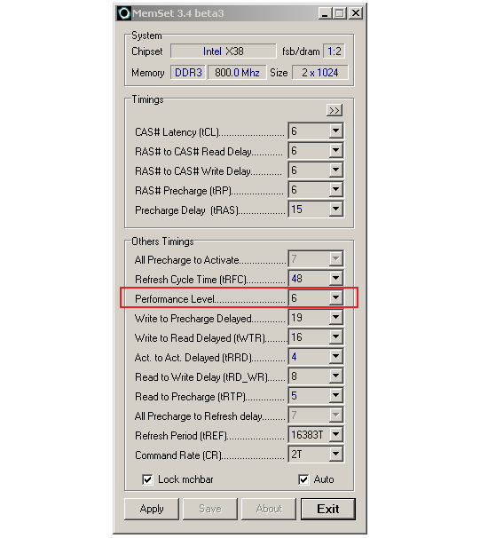
tRD in hiding…we promise we didn't make up the horrible "Performance Level" moniker
Arguably, the most important MCH setting when it comes to performance tweaking is the Static Read Control Delay (tRD) value. Like the memory CAS (CL), setting this value is relative to FSB. Case in point, a tRD value of 6, calculated in the same manner as used before, tells us that MCH sets a read delay of 15ns at an FSB of 400MHz. This means that in addition to the time required for the CPU to issue a request for data in memory to the MCH, the time the MCH spends translating and issuing the command to the memory, and the time the memory requires in retrieving the requested data, the MCH will spend an additional 15ns simply waiting for valid data to become available before fulfilling the CPU's original read request. Obviously, anything that can minimize this wait will be beneficial in improving memory read bandwidth and quite possibly overall system performance.
Until recently, direct tRD manipulation by the user was not even possible. In fact, for the longest time BIOS engineers had no choice but to accept this setting as essentially "hard-coded", making MCH performance rather lackluster. The only way to increase memory subsystem performance was to run at higher FSB settings or tighten primary memory timings. At some point, the MCH design teams got tired of the CPU people hogging all the glory and in a well-calculated effort to boost MCH performance exposed this setting for external programming.
The outside world's first introduction to variable tRD settings came when a few overclockers noticed that setting lower MCH "straps" allowed for higher memory bandwidths. What they didn't know at the time was that they had unintentionally stumbled upon tRD. Tricking the motherboard into detecting an installed CPU as an 800 FSB (200MHz) part forced the MCH into setting a lower tRD value than if the FSB were 1066 (266MHz). Consequently, overclocking the system to the same higher FSB value with the lower strap setting yielded higher memory performance. Often times the effect was significant enough that real-world performance was higher even with a lower final FSB. The tradeoff was apparent however: a lower strap meant a lower maximum FSB. The MCH tRD value, just like a memory timing, must eventually be loosened in order to scale higher. What's more, as is the case with memory, additional voltage can sometimes allow the MCH to run with tighter "timings" at higher speeds.
Eventually the inevitable next step in memory performance tuning became a reality. The option to adjust tRD independent of MCH strap selection became part of every overclocker's arsenal. Nowadays the MCH strap setting does little more than determine which memory multiplier ratios are available for use. Although tRD adjustments are now possible in many BIOS implementations, some motherboard manufactures choose to obfuscate their true nature by giving the setting confusing, proprietary names like "Transaction Booster" and the like. Don't let these names fool you; in the end they all do the same thing: manipulate tRD.
Tuning Memory Subsystem Performance
Earlier, we talked about the importance of first testing your motherboard's memory subsystem before moving to the CPU. When you think about it, the reason is clear. Encountering an error while testing blindly provides absolutely no helpful information as to the source of the problem. Since both the CPU and memory stability are dependent on the FSB it only makes sense that we remove them from the equation and first tune our motherboard at our target FSB. This is accomplished by setting the target FSB (we recommend you start at 400 MHz) in the BIOS, making certain to select a CPU multiplier which places the final processor frequency at or below the default value. Next, loosen up all primary memory timings and set the memory voltage to the modules' maximum rated value. Assuming the system is in good working order, we can now attribute all observed errors to discrepancies in the MCH settings and nothing else.
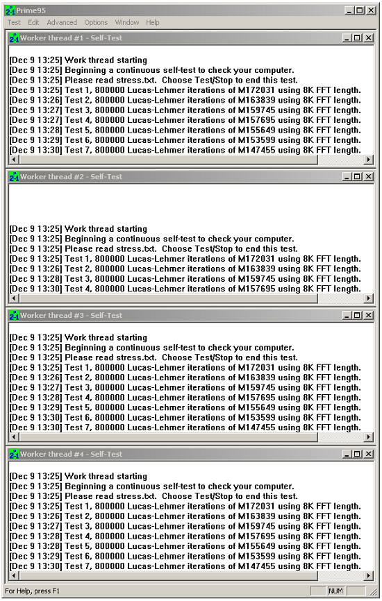
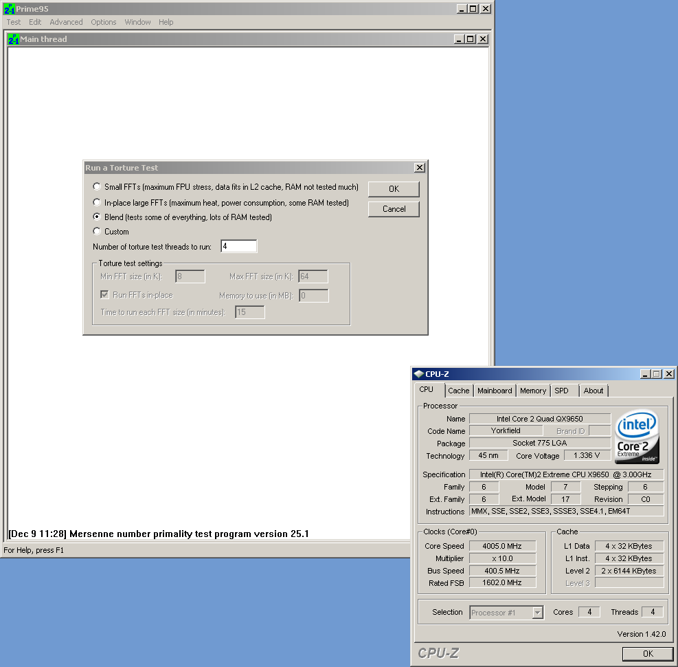 Preparing to run Prime95's blend test for the first time |
Boot the system in Windows and launch an instance of Prime95. From the menu select "Options" then "Torture Test…" and highlight the option to run the blend test (default). Now click "OK" to start the test. The blend test mode runs larger FFT values, meaning the processor must rely heavily on the memory subsystem when saving and retrieving intermediate calculation results. Although a true test of system stability would require many hours of consecutive testing, in the interest of time let the program execute for a minimum of 30 minutes.
If you encounter no errors (and the system is indeed still running), you can consider the memory subsystem "stable" at this point. If this is not the case, exit Windows, enter the BIOS, and try slightly increasing the MCH voltage. Repeat this process until you find you can complete (at least) a 30 minute run with no errors. If for some reason you find that increasing the MCH, voltage continues to have no effect on stability, or you have reached your allowable MCH voltage limit, you may be attempting to run the MCH higher than what is achievable under stable conditions. Setting Command Rate 2N - if available in the BIOS - loosening tRD, or removing two DIMMs (if you are running four) may help. If you find modifications to those items allows for completion of an initial Prime95 test, be sure to continue the testing by reducing the MCH voltage until you find the minimum stable value before moving on.
On the other hand, if you find that you can comfortably complete testing with additional MCH voltage margin to spare then you are in a good position to dial in some extra performance. Whether or not you wish to depends on your overall overclocking goal. Generally, more performance requires more voltage; this means more heat, higher temperatures, and increased operating costs. If efficiency is your focus, you may wish to stop here and move on to the next phase in tuning. Otherwise, if performance is your only concern, decreasing tRD is a great way of improving memory bandwidth, albeit usually at the expense of a higher MCH voltage.
In the end, as long as the system is stable, you are ready to move on to the next step. The insight necessary to determine just what to change and the effect if will have on stability and performance is something that comes only with experience. We cannot teach you this and experimenting further at a later time will help you sharpen these skills.
Select a Memory Divider and Set Some Timings
The latest generation of Intel memory controllers provides a much more expansive choice in memory dividers than ever before. That said, there are only three that we ever use, the most obvious of these being 1:1. Setting 1:1, simply put, means that the memory runs synchronously with the FSB. Keep in mind though that the FSB is quad-pumped (QDR) and memory is double data rate (DDR). For example, setting an FSB of 400MHz results in a 1.6GHz (4 x 400) effective FSB frequency at DDR-800 (2 x 400), assuming your memory is running 1:1. Selecting 5:4 at an FSB of 400MHz sets a memory speed of DDR-1000 (5/4 x 2 x 400). The other two dividers we would consider using besides 1:1 are 5:4, and in the case of DDR3, 2:1.
Regrettably, there are rarely any real performance gains by moving to memory ratios greater than 1:1. While it is true that many synthetic benchmarks will reward you with higher read and copy bandwidth values, the reality of the situation is that few programs are in fact bottlenecked with respect to total memory throughput. If we were to take the time to analyze what happens to true memory latency when moving from DDR2-800 CAS3 to DDR2-1000 CAS4, we would find that overall memory access times might actually increase. That may seem counterintuitive to the casual observer and is a great example of why it's important to understand the effect before committing to the change.
Start your next phase of tuning by once again entering the BIOS and selecting a memory divider. As mentioned earlier, even though there are many choices in dividers you will do best to stick to either 1:1 or 5:4 when using DDR2 and 2:1 when running DDR3. Next set your primary timings - typically, even the worst "performance" memory can handle CAS3 when running at about DDR2-800, CAS4 to about DDR2-1075, and CAS5 for anything higher. These are only approximate ranges though and your results will vary depending on the design of you motherboard's memory system layout, the quality of your memory, and the voltages you apply. You may find it easiest to set all primary memory timings (CL-tRCD-tRP) to the same value when first testing (i.e. 4-4-4, 5-5-5, etc.), and as a general rule of thumb, cycle time (tRAS) should be set no lower than tRCD + tRP + 2 when using DDR2 - for DDR3 try to keep this value between 15 and 18 clocks inclusive.
Failure of the board to POST (Power On Self-Test) after adjusting memory settings is a strong indication that either: A) you've exceed the memory's maximum possible frequency - choose a divider that results in a lower memory speed; B) the timings are too tight (low) for the attempted speed - loosen the values and try again; or C) the particular frequency/timing combination is possible, but not at the voltage currently applied - raise the memory voltage. Not all failure to POST conditions will have a solution. Some motherboards simply refuse to run certain memory dividers and we're finding more and more memory modules these days that are just flat out incapable of running the tighter timings possible with the previous generation's products.
Booting to the Windows desktop is always a pretty good indication that you are at least close to final stable values when it comes to memory. Again, start Prime95 and run at least 30 minutes of the blend test. Failures, especially rounding errors, are strong indications of memory problems. If you encounter errors, reset the system and increase the memory voltage by a small amount, always remembering to stay within specified limits. If you continue to experience errors, regardless of memory voltage, then you should loosen the primary timings and continue the testing. Once you have managed to "prime" for 30 minutes or more you can move on to the final phase - overclocking the CPU.
Overclock That CPU
With the memory and memory subsystems out of the way, we are finally ready to see what the processor can do. Because we have already decided on our target FSB we must accept for the time being that our final CPU frequencies will be limited to discrete steeps equal to our FSB. This is by design and affords us the knowledge that any Prime95 errors met during our last testing phase come from the CPU and nothing else. As always, varying the processor's multiplier changes only the CPU frequency - if memory is stable at 8 x 400 then by definition it's also stable at 9 x 400. Assuming we have decided to run 1:1, in both cases, the memory continues to operate at DDR-800 regardless of CPU speed. Later you can tune your final clocks by adjusting the FSB if you so choose.
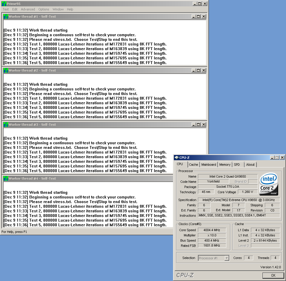 All green means everything is good. Remember to give the program time to run |
Once again, enter your motherboard's BIOS, this time adjusting only the CPU multiplier and the CPU voltage to set a potential overclocking frequency. Using custom water-cooling we were able to scale our QX9650 as shown below. Please note that all processors are different and voltage response curves generated using one CPU are not directly applicable to another. Your processor may perform slightly better or worse and these illustrations are only a general guideline. (The values shown are full-load CPU supply voltages and not the VID settings that we had to set.)
After booting to the Windows desktop, fire up Prime95 once again, this time choosing the option to run small FFTs as this setting places maximum stress on your CPU and leads to the highest load temperatures. As before, run at least 30 minutes while watching for errors. There are a few different potential failure modes, the least severe being a rounding error which causes one or more of the calculation threads to quit, changing the child window icon from green to red. Normally, with 45nm processors this is a good indication of a memory error, but since we know the memory is stable we can safely blame the CPU. In this case, the corrective action is to increase the CPU VID by a single step and try again. If the system freezes or freezes and then quickly resets, you will need to increase the CPU voltage by more than a single-step increment. Save yourself the hassle of multiple failures, increase CPU voltage by 0.05V or more, and try again. Later, back this down if possible until the CPU is just above the minimum required Vcore.
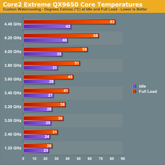
Depending on the cooling in use, you may find your overclock temperature limited. The QX9650 has a maximum thermal specification of 64.5°C but can generally handle temperatures as high as about 70°C before heat becomes a significant factor in scaling. Besides the core temperatures, the voltage regulator module (VRM) supply current can also function as a limiting factor. We saw before just how much current, in amps, the VRM circuit must provide under CPU full-load conditions in order to maintain stability. Current in excess of about 160A can be quite straining for even high-performance motherboards - make sure you adequately cool this area with at least a single, low-speed 120mm or larger fan if you plan to push a board this hard.
One of the great new features of the 45nm Core 2 family of processors is the ability to make use of non-integer multipliers. Sometimes referred to as half-multipliers, these values allow you to step your CPU frequency in increments one-half that of your FSB. Overclockers intent on running 400MHz FSB can now use a 10.5x multiplier to set a final CPU frequency of 4.2GHz, up from 4.0GHz (when 4.4GHz may be unachievable) without even touching the FSB. Consider this potential advantage if your motherboard allows use of these settings.
After some time experimenting with what works and what does not, you should start to get a feel for how your system responds to changes. During this time you should also learn how your CPU scales with voltage and exactly what speeds and timings to use with your memory subsystem. This three-phase approach helps lay the groundwork for the development of key overclocking skills and provides those new to overclocking with some ideas on how to approach the subject. Only once you understand the theory behind this basic methodology can you begin to safely stray into uncharted territory.
Benchmarking Results
| Intel Core2 Extreme QX9650 Overclocking Testbed | |
| Processor | Intel Core2 Extreme QX9650 Quad-core, 3.0GHz, 2x6MB L2 Cache, 9x Multiplier, 1333FSB |
| Comparison Processor | Intel Core2 Extreme QX6850 Quad-core, 3.0GHz, 2x4MB L2 Cache, 9x Multiplier, 1333FSB |
| Motherboard | Asus P5E3 Deluxe / BIOS 0703 |
| Memory | OCZ DDR3 PC3-14400 (DDR-1800) Platinum Edition |
| Memory Settings | 7-7-7-15 (DDR-1600 ~ DDR-1700), 2N |
| Cooling | D-tek FuZion CPU water block EK FC8800-GTX/Ultra full coverage GPU block ThermoChill PA120.3 radiator Dual Laing D5 pumps in series 1/2" ID (3/4" OD) Tygon tubing 6x Yate Loon D12SL-12 120x25mm fans @ 12v |
| Power Supply | Corsair TX650W |
| Video Card | MSI 8800 Ultra (660/1050) |
| Video Driver | NVIDIA ForceWare Release 169.12 (beta) |
| Hard Drives | 2x Western Digital 150GB (RAID 0) 10K RPM SATA 3Gbps 16MB Buffer |
| Operating Systems | Windows XP Professional SP2 (2GB) Vista Ultimate 64-bit (4GB) |
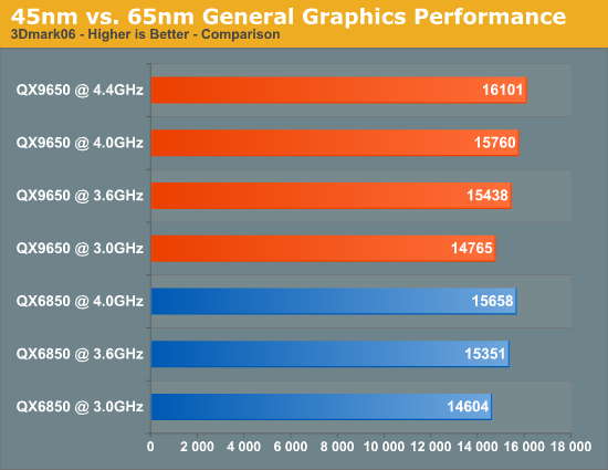
No overclocking review is complete without sharing the results of some standard benchmarking suites. The 3DMark series of benchmarks, developed and provided by Futuremark, are among the most widely used tools for benchmark reporting and comparisons. We measure Intel Core 2 Extreme QX9650 general graphics performance using 3DMark06, and because results from Windows XP and Vista are considerably different, we include both.
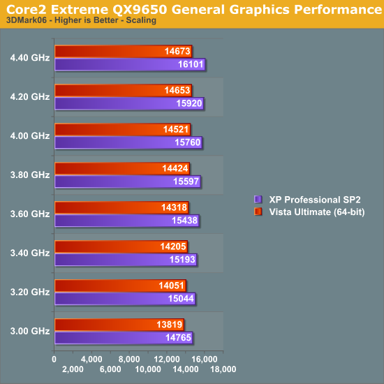
When we compare these results to those taken with a 65nm QX6850, we see clock-for-clock gains of less than 1%. However, the 45nm QX9650 is able to reach a much higher overclock of 4.4GHz, netting us enough improvement to push above 16,000 3DMarks without even altering our graphic card's stock clocks. At these speeds 18K+ with a single overclocked 8800GTX/Ultra is entirely within the realm of possibility (a score which we were in fact able to achieve).
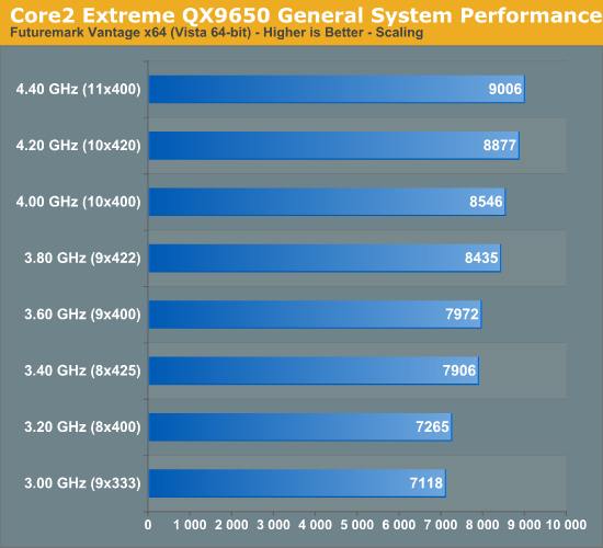
PCMark Vantage, Futuremark's latest system performance benchmarking suite, picks up where PCMark05 left off. Years in the making, this program offers the ability to test every conceivable aspect of total system performance either individually or all at once. Since Vantage only targets one operating system (Vista), we take advantage of the 64-bit executable included in the package running it in favor of the 32-bit file. Because Vantage (x64) is more of a complete benchmarking suite than the other tests we run, it makes sense that more than just pure CPU computing power influences results. For that reason, we have also shown the FSB settings used for each run. The additional memory bandwidth generated by the higher memory speeds does have an effect.
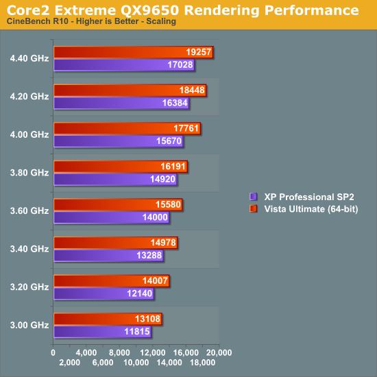
CINEBENCH R10 is another benchmarking program that performs radically different under both Windows XP and Vista. The developers at MAXON have done a tremendous job optimizing the code for 64-bit computing and it shows - unlike the graphics testing performed above, we find Vista maintains a clear advantage. As we can see, CINEBENCH R10 scales beautifully with additional cores and increased frequencies.
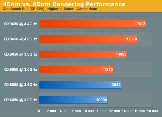
When placed together with results collected with a QX6850, the performance improvements offered by the QX9650 become immediately apparent. In this case, the Enhanced Core 2 processor is able to hold a commanding lead, thanks mainly to the massively improved frequency scaling.
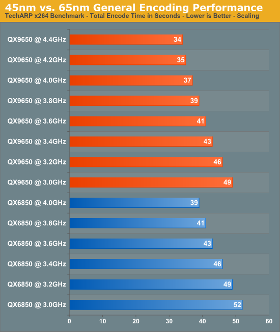
TechARP recently published a great x264 benchmark that essentially measures the time it takes a test system to encode a short, DVD-quality 720x480 progressive MPEG-2 video stream to a compressed, high-quality x264 file. Results are provided in the form of frames per second, and together with the known source file frame count it is possible to calculate the total encode time (shown below in seconds). The x264 CODEC makes very efficient use of multiple cores and is highly dependent on available processing power. As such, the benchmark makes a great choice for highlighting CPU performance. Although the CODEC does not yet include SSE4 optimizations, a new feature introduced with Penryn, the QX9650 has no problems making short work of our QX6850.
We hope to expand future testing to include real-world gaming results from some of the newest titles like Crysis, Call of Duty 4: Modern Warfare, Unreal Tournament 3, and Gears of War. Stay on the lookout for these results and others in our next look at the QX9650 when we pair this capable processor with the best motherboards companies like ASUS, Gigabyte, MSI, abit, DFI and Foxconn have to offer.
Final Thoughts
Although we cannot possibly go over everything there is to know about overclocking, we have definitely covered a lot of ground in a relatively short amount of time. We've looked at the QX9650's real power consumption figures, noting that the values published by Intel and AMD are not meant to exactly represent typical high-load scenarios. Studying just how the processor responds to more voltage shows us why we seem to reach a rather abrupt stop on the way up when overclocking.
We've also learned how rather than pushing a CPU to the ragged edge, sometimes it is better to find that point where performance and efficiency can co-exist in a delicate balance. A good overclock is not always about maximum speed. Instead, we would like to advocate what we call the "intelligent overclock" - find that point where going higher just doesn't make any sense…then simply stop and tune from there. We have provided many of the tools for doing so in this article; now it's up to you to make it happen.
With respect to the throttling issues we discovered during testing, we will not rest in our search for answers. It is unfortunate that we were able to find concern so early in such an impressive product. To some degree, this one has us scratching our heads; if our suspicions are correct, we may be looking at some rather drastic shifts in the cooling industry. As soon as we know more, so will you. In the meantime, we have seen nothing that would discourage us from recommending the Core 2 Extreme QX9650 to anyone that wants to experience the most that overclocking has to offer.
Intel's QX9650 is just the beginning - breakthroughs happen every day and design improvements will occur. After experiencing just how good 45nm is already, we cannot help but to be excited about what lies in store for us next. Cheaper 45nm processors like the Q9450 are at the top of our list, naturally, but we also eagerly await AMD's response to Intel's latest challenge. Can AMD reach 45nm and gain some similarly startling improvements? We can only hope!


