Original Link: https://www.anandtech.com/show/2374
ASUS Maximus Formula SE: X38 and DDR2 Unite!
by Rajinder Gill on November 9, 2007 7:00 AM EST- Posted in
- Motherboards
Overclocking with the ASUS Maximus Formula SE
For the vast majority of PC users, the announcement of a new CPU or chipset release generates a fair amount of interest, pegged with a realistic and thoughtful reaction towards the potential benefits (if any) over present hardware. Intel has forged ahead at such a pace this last year that it seems owning the performance crown for the foreseeable future is not even enough at this point. Releases of information from AMD about their future CPU and chipset plans have quickly been answered by Intel (with actual product releases in most cases) to ensure their continued market dominance in the enthusiast sector for the time being.
With this rapid release schedule comes improved fabrication methods that have brought many benefits: better speed scaling, lower transistor leakage, lower overall power consumption, and reduced production cost. These new CPU and chipset releases have also been coupled with competitive price cuts based on the competitive landscape that users have enjoyed the past 18 months. We have seen these improvements and strategies delivered with precision by Intel into the market place over the last year and a half while AMD has stumbled. If that's not enough, the upcoming release of the Penryn processor family features a CPU die shrink from the current 65nm process to 45nm along with additional cache sizes and several core improvements such as SSE4 support. This seems more than enough to guarantee an overall performance advantage over AMD for some time to come in the enthusiast sector.
The question from those steeped in conservatism is whether or not this industry will ever fully utilize the potential of current hardware before moving ahead to something new. From a corporate perspective, posing this question can be construed as completely naïve. Indeed, there's money to be had by making a series of small changes, while simultaneously holding a partially revealed trump card in current R&D, just in case there is the chance of a competitor counterstrike.
The Internet has become such a powerful marketing tool that a strategic selection of websites for a launch can create enough interest to guarantee a successful campaign, even when economically or performance wise a change might not be beneficial for the user. At this time, much of Intel's advertising success is accrued by placement of product in the hands of overclockers, who are enlisted to fulfill the role of presenting new hardware by showing gains in various synthetic benchmarks. This is a perfectly logical corporate decision - it is easier to sell new product to a group that is passionate about even the smallest gains than it is to satisfy the somewhat discerning real world PC user.
Since the launch of Core 2 Duo, we have shown that any company in support of Intel's CPU and chipset release strategy needs to have sufficient resources to co-exist with Intel's relentless marketing drive. This leads us to ASUS, who has managed to surf the Core 2 Duo wave to its full potential. They are usually among the first to release a motherboard with each Intel chipset launch, reaping the benefits of being one of the preferred launch partners for Intel chipsets. Most of the boards released by ASUS have attained substantial accolade for the most part, especially those priced in the sub $200 region. Further, there is ASUS's top of the line motherboards, the ROG (Republic Of Gamers) series. This particular product line is aimed to satisfy the needs of the upper tier gaming and overclocking enthusiasts.
Over the past year, we have seen several boards released bearing the ROG badge: the Striker Extreme, Commando, Blitz Formula, and Blitz Extreme. Most of these motherboards have been a popular choice for enthusiasts and gamers alike. Our own feelings about the ROG series is that ASUS has offered overall improvements in terms of overclocking friendly BIOS functions, component quality, features, unique on-board cooling designs, and in some cases improved compatibility - although not always. The ASUS Striker series was an especially finicky beast for non-QVL memory modules. Fortunately, the Intel chipset based boards are far friendlier in this department, a trend we hope continues with their latest products.
The latest addition to the "bells and whistles" ROG series is the ASUS Maximus Formula, based upon the Intel X38 chipset and featuring DDR2 memory support. To date, DDR2 performance using the X38 chipset has been a little underwhelming for us. Synthetic and real world benchmarks have shown little to separate X38 DDR2 scores from those using the P35 chipset. The motherboard suppliers should not be penalized for this situation as the X38 was certainly hyped to be the killer product for Intel's high-end aspirations. Our experiences with the X38 over the summer reminded us of a roller coaster ride with several highs but just as many lows as we tested each chipset revision and BIOS release. A month ago we were not excited about the X38, but with the BIOS releases maturing along with early performance results from Penryn we are ready to get back on the roller coaster.
Purchasing decisions often seem clear-cut, especially those based upon outright synthetic performance figures. Before we arrive at a conclusion today, let's look at some of the factors forcing/promoting use of the X38 chipset within selected markets (in this case the top-end enthusiast sector):
- Intel's CPU price/performance scaling strategy: Intel uses lower default multipliers for non-Extreme CPUs, demanding higher overall FSB potential from chipsets - especially for quad-core CPUs.
- Attaining the limits of economically viable engineering practices by using a separate memory controller hub: This creates the need to push towards DDR3 rather than trying to lower overall chipset latency and increasing memory bandwidth using current DDR2 technology. Using DDR3 and associated memory timing ranges can offer superior scaling potential; testing has shown increased synthetic benchmark scores and small gains in workstation and gaming software with the right memory. The obvious selling points of X38 in DDR2 format are suggested in points 1 and 3.
- Dual x16 PCI-E 2.0 support for upcoming AMD graphics solutions (RV670 to start) to improve CrossFire performance.
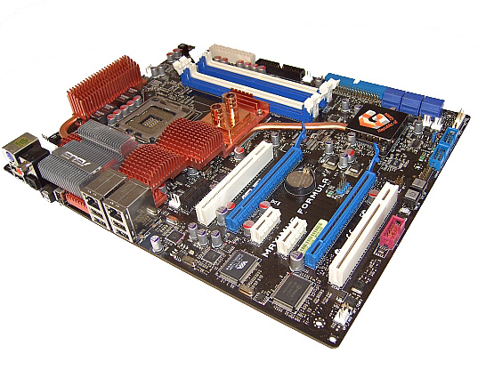
Board Layout and Features
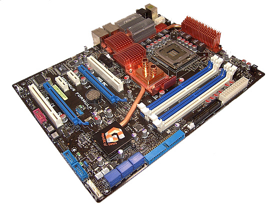
There are no surprises here; ASUS delivers the standard ROG color scheme consisting of blue and white slots, while sticking with the same overall layout we have seen in earlier ROG boards. There are eight on-board fan headers, which are controllable either through the BIOS or with the supplied PC Probe II software via the OS. The three OPT fan headers have probe connectors situated nearby and are compatible with probe related fan speed controls (the probes are sold separately). The whole board utilizes solid polymer capacitors, which are mandatory on the ROG series.
ASUS has also included a "Volt Minder" system that uses traffic light colored LEDs placed near the CPU, Northbridge, and Southbridge. These LEDs light up to signal the level of voltage applied; Green is safe or normal range, yellow for high voltage, and red is referred to as "crazy voltage levels" by ASUS - rightly so when you look at the available levels of voltage to these areas in the BIOS. Overall, the general layout, features, and slot placement is ideal for an overclocking oriented motherboard.
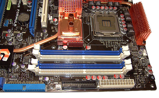
The DIMM sockets are located a little lower on this board; ASUS has moved the slots closer to the Northbridge, shortening the PCB trace lengths (in theory reducing inductance and signal crosstalk). We had no issues inserting or removing our 4x1GB memory modules from the DIMM slots, even with a long graphics card inserted into the primary PEG slot. Memory voltage is supplied by a two-phase power circuit, which has become another ROG motherboard trademark. With 4GB of memory becoming increasingly popular, the lower impedance should help sustain stable high MHz memory clocking. The 24-pin ATX header is located conveniently at the edge of the board, alongside the floppy drive and a fan/probe connector, all accessible without hindrance from other components.
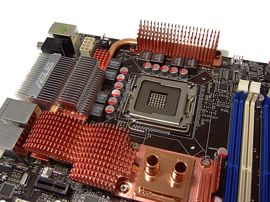
CPU power is supplied by an eight-phase analog PWM circuit, using high quality Yageo inductors. The 8-pin 12V connector is located at the top left corner of the board, just behind the PS/2 connectors. This board is clearly aimed at users who are likely to water-cool both the CPU and Northbridge. Mounting air coolers that use thumbscrews for attachment is made a little awkward by the close proximity of the large Northbridge heatsink around the lower left corner of the CPU socket. A fan header is placed at the top edge of the board. We also have an SPDIF output header, and the top left of the board is home for the supplied LCD post display connector. Thankfully, ASUS listened to users and the LCD post display comes with its own cable allowing for user-selected placement.
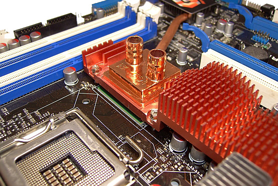
Moving on, we find the elaborate ROG heatsink designs ASUS employs to cool the Northbridge, Southbridge, and PWM areas. For the Maximus Formula SE, ASUS has employed a hybrid design consisting of a water block that is spot epoxy glued to a large heatsink that connects the Southbridge and Northbridge together with a heatpipe. The heatpipe continues further, covering part of the separate PWM heatsink, with an Aluminum fin section. A small fan is supplied that clips onto the Aluminum section of the heatsink, helping to cool the Northbridge and we suggest using it.
ASUS supplies both 3/8" and 1/2" tubing adaptors together with spring clamps to hold tubing in place. Unfortunately, our high flow pumps (Petra Top DDC Ultras) were too much for the 1/2" spring clamps. Using the supplied 1/2" clamps, our tubing actually came loose and shot off the barbs. Bottom line: screw type hose clips are a safer bet for high-pressure water cooling pumps. Initial testing with the stock solution using our upper-end water-cooling solution showed little temperature gains over air-cooling using 2x120mm fans over the area. During testing our water block actually came loose, and we were a little surprised to find that there was little contact between the heatsink and NB water block. No thermal paste was used in the stock design to ensure contact between the spots of epoxy glue that had been used to bond the two surfaces together.
Because there was very little contact between the Northbridge water block and the heatsink, it's no wonder there were no initial gains from using water-cooling. We re-attached the block using a combination of thermal paste (in the center of the block) and epoxy (around the perimeter). We also checked the contact between the chipset IHS (Integrated Heat Spreader) and the Northbridge heatsink assembly. The footprint left by the pad showed around a 60% contact surface, with the center of the NB IHS making very little contact with the heatsink. We scraped away the flaky thermal pad and used thermal paste in its place. The increased surface contact of the two modifications lead to a ~9C drop in load temperatures and certainly helped in overall board stability when overclocking. Needless to say, this is not the sort of thing users should be required to do on an "extreme" motherboard. Hopefully ASUS can improve their process and quality control on this aspect of the Maximus. In fact, ASUS has shipped us a new board that should arrive shortly so we can compare early production process to the current one.
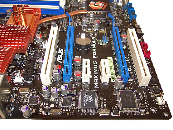
There are two PCI-E 2.0 x16 slots, both offering full x16 bandwidth for dual graphics cards. The remaining slots are three PCI-E x1 (the black slot is reserved for the supplied SupremeFX II ADI based 8-CH Audio card), and two PCI 2.3 slots, placed in between the PCI Express slots. The wide PCI Express slot spacing should help airflow, especially with high heat producing cards such as the AMD HD 2900 series. Underneath the lower PCI slot, we have a fan and thermal probe header. Further to the right we have an on-board 1394a port connector and power and reset switches. One of the Internal USB connectors is placed over the lower PCI Express x16 slot; the other two internal USB connectors are situated to the right of the power and reset switches.
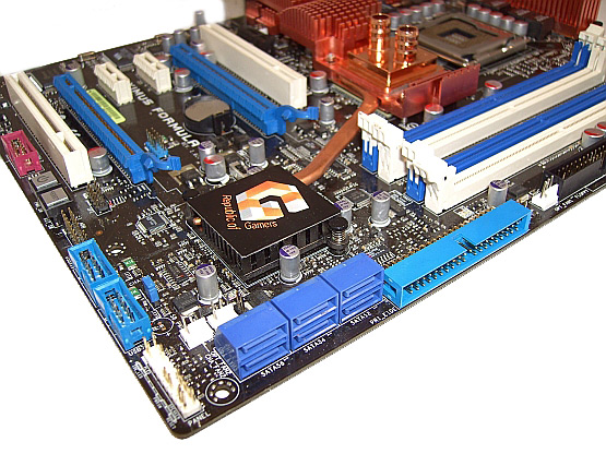
The Intel ICH9R Southbridge has the standard six on-board SATA sockets, placed at a 90 degree angle towards the right edge of the board. If the motherboard is to be mounted in small PC cases, it is wise to plug the SATA cables in before securing the motherboard into the case. Underneath the SATA ports we have the system panel connector, featuring ASUS' easy mount Q-Connector system. Two more fan headers and a thermal probe header sit behind the SATA ports.
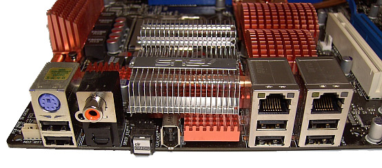
Rear IO ports feature a PS/2 keyboard port with 2 USB slots directly underneath; users with a PS/2 mouse will need a PS/2 to USB adaptor. A Coaxial S/PDIF output is also present, together with a TOSLINK output. To the right we have the Clear CMOS button, making it easy to clear the CMOS after the board is installed in a case. There is a rear FireWire port, dual Gigabit LAN (featuring teaming support), and four additional USB ports. ASUS also bundles 3DMark06 (Advanced Edition), STALKER, and Kaspersky anti-virus software with the board.
Test Setup and Overclocking Results
| ASUS Maximus Formula Standard Testbed |
|
| Processor | Intel Core 2 Quad Q6600 (QX6800 at 9x multiplier and OC Test) Quad Core, 2.4GHz, 8MB Unified Cache, 9x Multiplier, 1066FSB |
| CPU Voltage | 1.2500V |
| Cooling | Tuniq Tower 120 |
| Power Supply | OCZ Pro Xstream 1000W |
| Memory | OCZ Flex PC2-9200 (4x1GB) |
| Memory Settings | 4-4-4-12 (DDR2-1066) |
| Video Cards | MSI HD 2900XT for P35 comparison, MSI 8800 Ultra for OC Tests |
| Video Drivers | AMD 7.10, NVIDIA 163.75 |
| Hard Drive | Western Digital 7200RPM 750GB SATA 3/Gbps 16MB Buffer |
| Optical Drives | Plextor PX-755A |
| Case | CoolerMaster Stacker 830 Evo |
| BIOS | ASUS 0505 |
| Operating System | Windows Vista Ultimate, Windows XP Professional SP2 |
| . | |
We decided to use our base QX6800 CPU with our standard tests run on the 9x multiplier to simulate the attractively priced Q6600 CPU and to match previous benchmark results. In this section of testing, we aim to remain within realistic cooling capacity temperatures and current CPU stepping capabilities. This better shows an overall picture of motherboard performance potential, using widely available parts. Once again, Micron D9GKX based memory modules do not show outstanding results, requiring high voltages for stability on both our P35 and X38 based boards. We decided to stick with our D9GMH based OCZ Flex 9200 modules, as they seem to perform well on current P35 and X38 motherboards.
With such a vast array of overclocking BIOS functions at our disposal, a decision was made to stick with a single operating system environment. Microsoft XP SP2 was chosen due to its maturity, taking away some of the time burden looking for possible software level conflicts that may exist on a newer OS (though we ventured to run our standard Vista test suite for the non-overclocking benchmarks). This does not mean the board cannot work with Vista at present when overclocking; we are just trying to eliminate possible downtime on non motherboard/BIOS related issues. There's also the fact that a vast majority of overclocking enthusiasts have not switched to Vista (yet).
High and medium resolution 1920x1200, 1600x1200, and 1280x1024 game benchmark tests were run in order to cross-compare CPU MHz related gains in our board specific tests. We utilize new drive images on each board in order to minimize any potential driver conflicts. Our 3DMark results are generated utilizing the standard benchmark resolution for each program. We run each benchmark five times, throw out the two low and high scores, and report the remaining score to reflect a repeatable average.
Our cooling preference for pushing past 3.6 GHz with a quad-core CPU for 24/7 use is to move to water-cooling. The following water-cooling components are used in addition to our basic test components when overclocking:
Swiftech Apogee GTX CPU water block
2x Petra Top Laing DDC Ultra water pumps in series
Swiftech Micro-Res
Thermochill PA120.3 Radiator, with 3x Panaflo 120mm fans
Danger Den 1/2" ID Tubing
We limited our standard Vista test suite to a few benchmark results to indicate the general performance of this board when compared to current P35 motherboards. Since ASUS Maximus Formula was designed for the overclocker and gamer in mind, not your typical YouTube viewer, we decided to take a different look at this board and focus on overclocking for this particular article with results compared to the DFI P35 motherboard. We will expand our benchmark results to include direct comparisons to other X38 motherboards in a future roundup.
Synthetic Graphics Performance
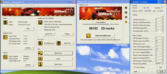
The 3DMark series of benchmarks developed and provided by Futuremark are among the most widely used tools for benchmark reporting and comparisons. Although the benchmarks are very useful for providing apples-to-apples comparisons across a broad array of GPU and CPU configurations, they are not a substitute for actual application and gaming benchmarks.
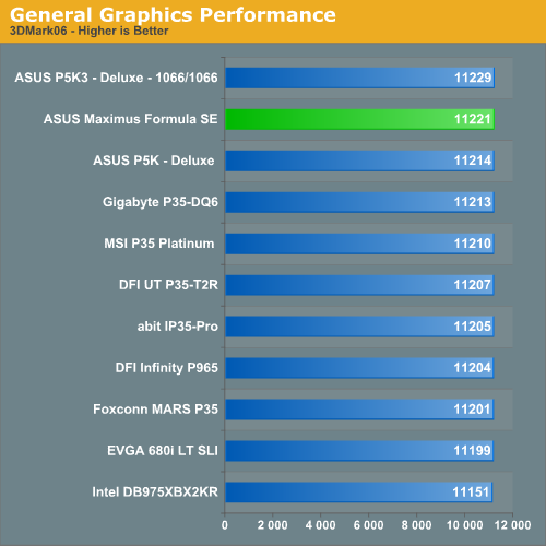
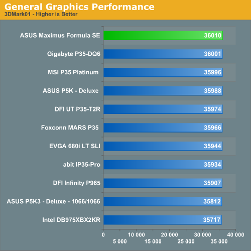
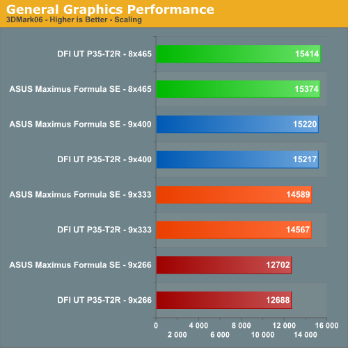
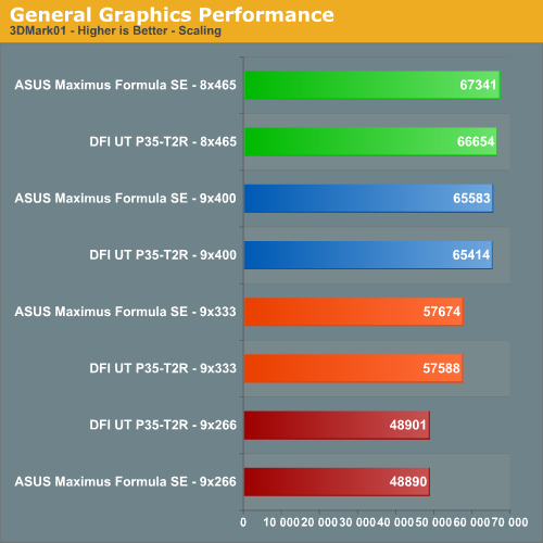
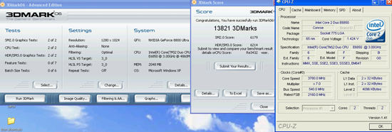
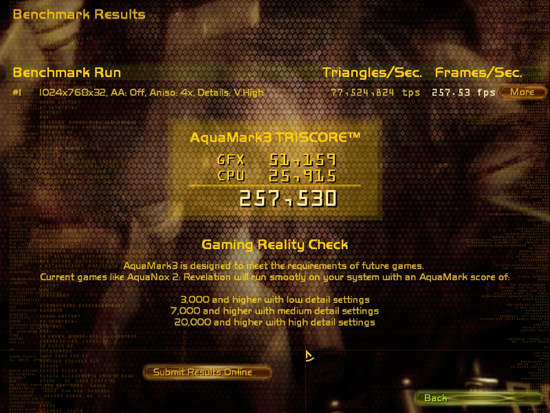
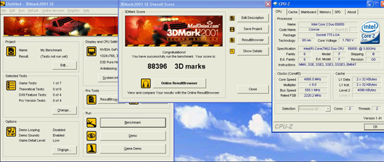
In our 3DMark06 test, the DDR2 based boards are basically even in this test. The ASUS Maximus board did not exhibit any issues during repeated testing in this CPU/GPU intensive test. In the more memory and CPU sensitive 3DMark01 benchmark we see our Maximus board generating the top mark. The differences in performance are not really noticeable in either 3DMark unless you're looking to reach the top of the ORB. That of course requires some serious overclocking, which this board is capable of doing.
General System Performance
The PCMark05 benchmark developed and provided by Futuremark was designed for determining overall system performance for the typical home computing user. This tool provides both system and component level benchmarking results utilizing subsets of real world applications or programs. We consider the PCMark05 benchmark to be both synthetic and real world in nature, and it provides for consistency in our benchmark results.
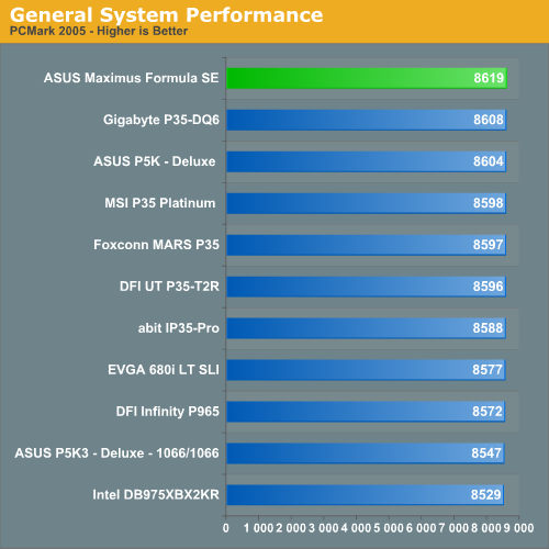
Our PCMark05 scores mimic the results from our 3DMark benchmarks with differences between the boards not exceeding 2%. The ASUS Maximus board finishes first. While this benchmark is designed around actual application usage, we will see if these results mirror our own application testing.
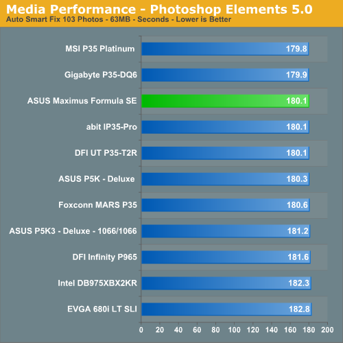
Media Performance
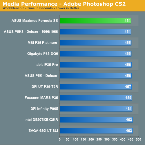
We will take a brief look at general media performance with our test suite that includes Adobe Photoshop CS2 and Adobe Photoshop Elements 5.0.
We utilize the PC WorldBench 6.0 Test for measuring platform performance in Adobe's Photoshop CS2. The benchmark applies an extensive number of filters to the test image and heavily stresses the CPU and storage systems. The scores reported include the full conversion process and are represented in seconds, with lower numbers indicating better performance.
Our next test is one recommended by Intel, but the test itself appears to be fair and results are very repeatable. This test simply measures the amount of time required to fix and optimize 103 different photos weighing in at 63MB. Time is measured in seconds, with lower times resulting in better performance.
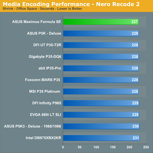
Media Encoding Performance
We are utilizing Nero Recode 2 for our video encoding test. The scores reported include the full encoding process and are represented in seconds, with lower numbers indicating better performance.
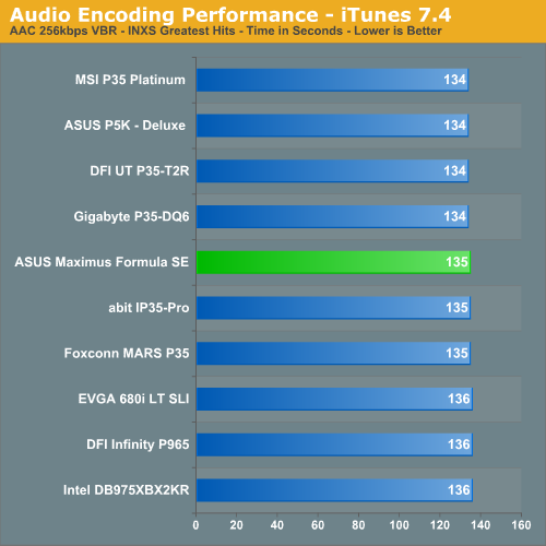
Audio Encoding Performance
We will utilize iTunes 7.4 for our audio encoding tests as it is one of the most utilized audio applications available due to the immense popularity of the iPod. As in previous articles, we are using an INXS Greatest Hits CD for testing, which contains 16 tracks totaling 606MB of songs. We use iTunes to convert our WAV files into an ACC compatible format. We utilize the 256kbps and variable bit rate option.
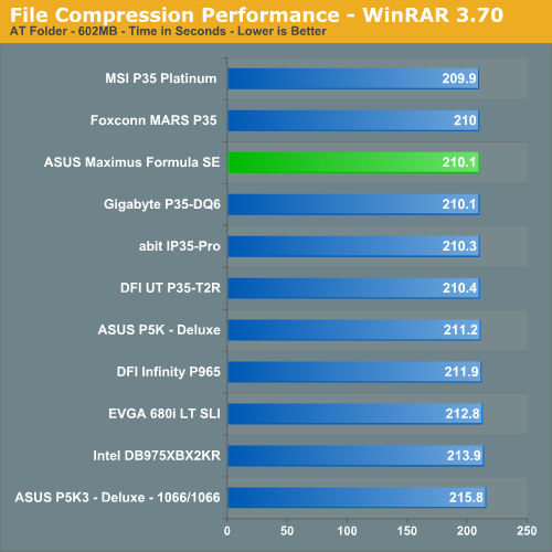
File Compression Performance
Another CPU crunching utility is WinRAR 3.70, which provides for computationally intensive file compression. Our test folder contains 444 files, 10 subfolders, and 602MB worth of data. All default settings are utilized in WinRAR and our hard drive is defragmented before each test
Performance Summary
Yet again, the ASUS Maximus Formula performs very well in tests that depend on fast CPU/memory throughput. It doesn't place first in every test, but it does place near the top and there aren't any apparent issues with its performance in any of the tests.
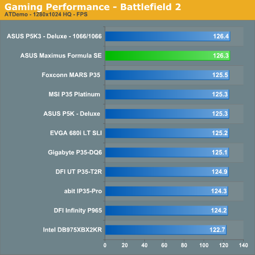
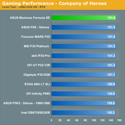
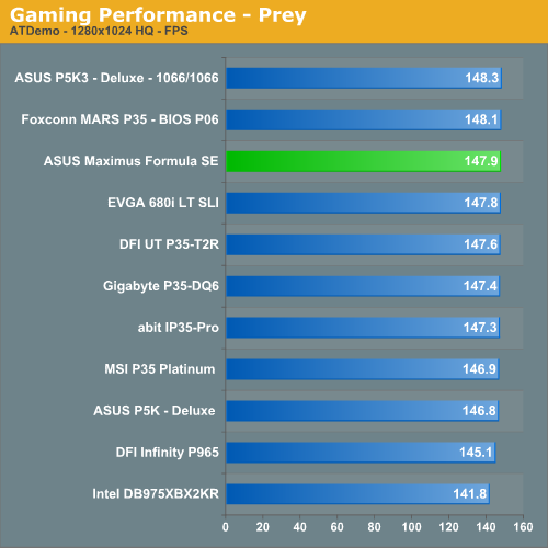
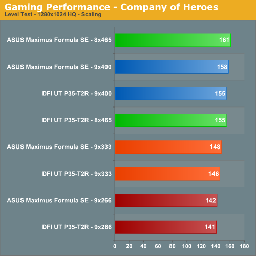
Gaming Performance
As usual, gaming performance was tested with a variety of current games. We ran our benchmarks at a 1280x1024 resolution with high quality settings.
Gaming Summary
The ASUS Maximus performed as expected in our gaming tests. The board performed very consistently in these particular tests. Our initial tests with the latest game releases (UT3, Crysis, HellGate London) show the X38 chipsets performing the same or slightly better than the P35 chipset. We will have CrossFire performance results utilizing the HD 2900XT card in the roundup but at this time the X38 chipset performs anywhere from 3% to 18% better than the P35.
Synthetic Benchmark Performance
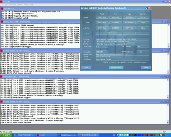
Everest Cache and Memory Benchmarks
9X266
9X333
9X400
8X465
8X465 DFI LP UT P35 T2RG
Our 8 hour Prime95 torture test run ended at 450FSB; 460-465FSB provided around 1 hour of torture test stability and allowed us to complete all benchmarks but Prime95. The same CPU and components managed 465FSB on the DFI P35 T2R, but with a far longer 11 hour Prime95 torture test pass - without any failures. Unfortunately, the ASUS 0505 BIOS does not provide sufficient GTL tweaking ability to extend CPU core stability. To get the board close to P35 DDR2 performance we are limited to the 400 NB strap and 3:4 memory divider ratio. At higher FSB points, the 400 NB setting is the only strap that is stable enough for 24/7 use. This makes it quite apparent that Intel's engineering favors 1600FSB support and DDR3 for the X38 and future processors. DFI P35 results have also been added at 465x8. The only way to run the Maximus Formula in a fully competitive manner is to run the memory in excess of 1200MHz, which limits users to top-end DDR2 modules.
The DFI board runs DDR2-1120 very happily at low VDimm with the right modules; the Maximus is limited to either the 1:1 or 3:4 using the 400 NB strap. Using 1:1 would have limited memory speed to DDR2-930 on the Maximus, which is quite low unless you run CAS 4-3-3 timings. Such low latency timings required a very high VDimm, and 1N did not seem to work at this speed either, so we chose to stick with DDR2-1240 CAS 5-5-5-15, which was possible at a reasonable 2.2V.
Overclocking Performance Comparison
Synthetic Graphics Performance
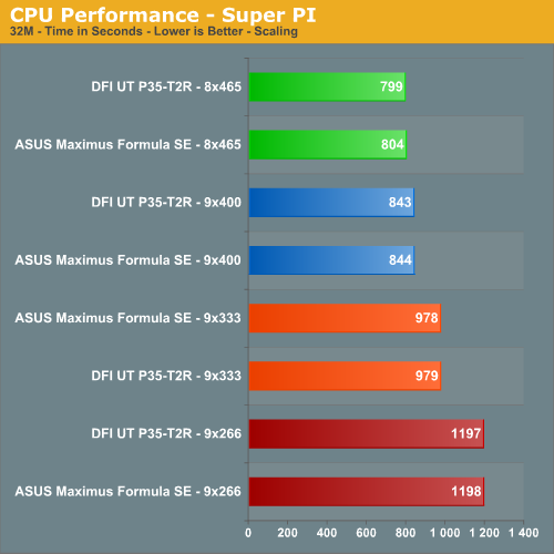
CPU Performance
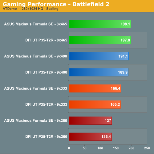
Gaming Performance
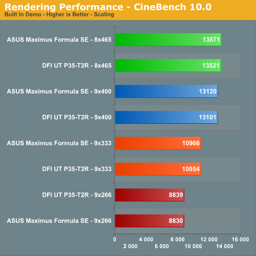
Rendering Performance
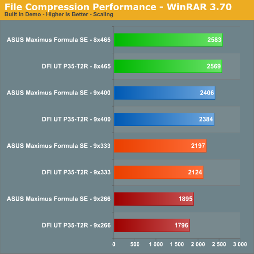
File Compression Performance
The results are very close, with the Maximus just passing the DFI board in 3D benchmarks, but only by minimum values that are nothing to crow about. With figures this close, it is fair to say the margin of error between benchmarks and even variance in XP installations (when we take user systems into account) could easily reverse the overall standings. For single graphics card use, a top-end P35 based motherboard is perfectly capable of providing almost identical benchmarking figures and in some cases surpassing the X38 boards at this time.
However, we have seen significant improvements in memory performance with each succeeding BIOS release so there may be hope for the X38 chipset to distance itself from the P35 in DDR2 performance. Our take is that we might end up seeing a 1%~3% overall difference at most. Probably just enough for the suppliers to start replacing their high-end P35 motherboards with the X38 variants in order to eliminate product overlap. While this is not bad, it is a disappointment to us after the early hype surrounding the chipset. In fact, our A0 X38 silicon based reference board still performs better that the retail boards but not by much now.
We must emphasize that the DFI board is actually more "stable" at 465FSB; also DDR2-1120 is a little easier to reach with more attractively priced memory modules. Had we used the lower 1:1 divider on the Maximus, the scores would have been reversed. In truth, using the 1:1 divider on either board should only reduce scores by around 1-2% maximum, making some of the cheaper DDR2-1000 capable modules a wise purchase for a workstation or gaming PC. ASUS is currently working on a BIOS release that improves overclocking and we will report any performance changes shortly.
Air-Cooled and Subzero Benchmarks
| ASUS Maximus Formula Overclocking Testbed |
|
| Processor | Intel Core 2 Duo E6850 - G0 Stepping Dual Core, 3.0GHz, 4MB Unified Cache, 9x Multiplier, 1333FSB |
| CPU Voltage | 1.300V Base |
| Cooling | Various - Tuniq Tower, Dual Rotary Cascade |
| Power Supply | PCP&C 1200W |
| Memory | OCZ Flex PC2-9200 (2x1GB) |
| Memory Settings | 4-4-4-12 (DDR2-1066) |
| Video Cards | MSI 8800 Ultra @ 702/1205, EVGA 8800 GTX 830-861/1000 |
| Video Drivers | NVIDIA 163.75 |
| Hard Drive | Western Digital 7200RPM 250GB - WD2500KS |
| Optical Drives | Plextor PX-755A |
| Case | Dimastech benching table |
| BIOS | ASUS 0505 |
| Operating System | Windows XP Professional - SP2 |
| . | |
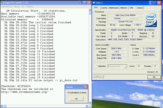
ROG boards are designed to be raced (the extreme voltage ranges in BIOS hint at this), after "realist" testing. Any performance review is incomplete without taking at least a small benchmarking test drive with the pedal to the metal. We decided to find out just what the board would do with a "handpicked" E6850 CPU that is capable of high FSB speeds. Using air-cooling we managed to boot at 550FSB (3.85GHz), but did not manage to hold Super PI 32M stable using the 400 strap and 1:1 divider with 4-4-4-10 memory timings. We settled for 540FSB (3.78 GHz), again with the 400 NB strap using the 1:1 divider. Here are a few benchmark results:
E6850
Using cascade cooling on both the CPU and GPU allowed benching in the region of 550-560FSB using the 9x multiplier. tRD (Performance Level) had to be set quite loose at 11-12 to provide stability for the benchmarks to pass. This is another area where ASUS is implementing core BIOS level changes to improve stability and memory performance in the higher FSB ranges. The DFI P35 board also reached 550FSB with this CPU but we were not able to hold the 550FSB level over the course of testing. We had to back off to the 540FSB range. This is the one key difference we have noticed between the two chipsets, the X38 will hold a higher FSB level over the course of extreme benchmarking than the P35.
QX6800
The Maximus Formula is certainly capable of holding high FSB/CPU MHz levels for extreme benchmarking. We also gave our cold bugged QX6800 G0 a little test spin with four cores active for a 3DMark06 session; unfortunately we were limited to around a 4400MHz CPU speed. This is not a problem with the motherboard; the CPU itself has been tested on many different boards with the same CPU MHz wall. These results surpass our DFI P35 slightly, indicating to us that the X38 is finally starting to mature and this board is a solid choice for overclocking, especially with a dual-core processor.
Important BIOS Functions
We have picked out a few of the more important BIOS functions for a breakdown of their use and application. The "Advanced Tweaker" BIOS screen has quite a few secondary memory timing options; for the most part these can be left to board/SPD default values. We are providing the best "bang for the buck" manual settings below.
AI Overclock Tuner:
Set this function to manual for overclocking; the Auto function enables preset overclocks automatically when the system is under load.
OC from CPU Level Up:
ASUS enabled overclock profiles based upon the processor type in use; for manual overclocking this function may be left at Auto. If low level automatic preset overclocking is preferred, select either the CPU type or "Crazy" mode. Setting either of the latter two options adjusts all board voltages to preset values. The preset values themselves can be higher than is absolutely necessary for the applied overclock. The Auto overclock functions can be useful for beginners who are getting to grips with overclocking, with the option to move to manual overclocking later. We suppose this guarantees stability via a somewhat brute force approach. For long-term use we recommend using a manually set overclock.
FSB Strap to Northbridge:
The two straps of use for overclocking past 400FSB are 333 and 400. All other straps have lower FSB limits.
PCI-E Frequency:
If the ICH9R SATA ports are used then a setting around 115mhz is safe, though scores do not seem affected by the minimum 15mhz overclock. We noticed anything over 118MHz would cause problems with the drives or even the POST routines. Benchmarkers as usual are best advised to use an IDE drive, turn off all the peripherals, and then try to maximize the bus speed.
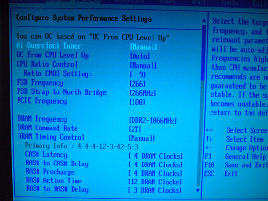
DRAM Frequency:
Available dividers are dependent on the FSB strap to Northbridge setting. For 333 we have 1:1, 5:6 and 5:8, while for 400 we have 1:1 and 3:4 memory divider ratios. Best overclocking results and performance are available from the 400 NB setting using the 3:4 divider. Access latency and overall bandwidth seem to reach their peak using the 400 NB strap around 450FSB and upwards with DDR2-1200 memory speed.
DRAM Command Rate:
Sets either 1N or 2N memory timing. 1N has a low memory MHz range (900MHz and under), useful only for the 1:1 divider. 2N is the preferred choice for outright performance when using good DDR2 at speeds greater than 900MHz.
DRAM Timing Control:
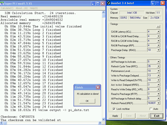
Set this to Manual to obtain control of all primary and secondary memory timing ranges. The BIOS shows primary and secondary timings above both respective sections. Users may wish to enter the shown timings manually for each setting and then experiment with tighter timings where possible. The board defaults are generally tight enough for 24/7 use. For benchmarking Memset allows access to setting ranges not accessible in BIOS.
The following three settings are all amalgamated from tRD, tRD Phase adjust, and chipset performance registers areas that are fully unlocked on DFI boards. Rather than direct fine control, ASUS prefers an auto manipulation of preset combinations, with a limited user set range. Results are fairly average using relaxed combinations. The X38 chipset itself seems to favor 333 and 400NB straps, which in turn limits the range of use of ASUS' spin on these settings. We look at possible setting ranges below.
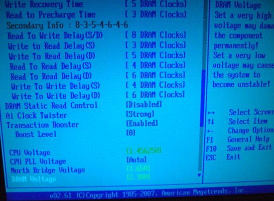
DRAM Static Read Control:
This function is best set to "Disabled" for high FSB levels (450 FSB upwards). "Enabled" gives a small gain in memory access latency at the expense of overall stability. We believe this setting alters a single TRD phase to low; performance advantages either way are not stellar.
AI Clock Twister:
We recommend use of the "Strong" setting wherever possible. Setting "Weak" reduces overall bandwidth and access latency. "Strong" brings the x38 chipset performance almost in line with the P35 using DDR2 memory. Please note, we did not find setting "Weak" worked well with the 400 NB strap at 465FSB.
Transaction Booster:
Ranges here are from 0-7 (0-3 are stated as usable in BIOS), with either the "Enabled" or "Disabled" setting. The 0 setting with either "Enabled" or "Disabled" selects the default tRD level for the NB strap and memory divider combination. The Enabled function lowers tRD (tRD -1) and/or tRD phases with each additional digit over 0, meaning an upward scale increase or boost is more aggressive with Transaction Booster set to Enabled. If using the 333 NB strap, set Transaction Booster to Disabled and use either 0 or 1 as the "Relax level" setting. When using the Relax setting range (Disabled Transaction Booster), using higher numbers will increase tRD (tRD +1) and tRD Phase adjust for lower overall performance, allowing access to higher FSB speeds. For quad-core overclocking the 400 NB strap performs best with Transaction Booster set to Enabled and 0 as the Boost Level setting - unless you're chasing higher FSB speeds at the expense of overall performance. Dual-core CPUs capable of high FSB speeds may use the "Relaxed" setting of 3 if outright FSB speed is the goal.
CPU PLL Voltage:
Scale range is 1.5-3V in 0.02V increments. Stock is 1.5V, although overvolting can bring small increases to FSB limits. We do not recommend using past 1.75V for long-term use.
North Bridge Voltage:
Scale range is 1.25V-1.85v. Stability is greatly affected by NB temperatures, and temps over 47C are prone to failures during longer Prime torture test runs. Active cooling of the NB is recommended for overclocking. A combination of air and water-cooling generates the best results when using the stock ASUS water block and heatsink combo. Voltages around 1.61V-1.65V are required for overclocking past 440FSB.
DRAM Voltage:
ASUS provides us with a searing 1.8V-3.4V scale. The board does overvolt the BIOS setting by around 0.04V, and users are advised to subtract this value from the BIOS setting to stay within warranty voltages for memory ( yes, we said that with a straight face).
Loadline Calibration:
Available options are Auto, Disabled, and Enabled. Use "Enabled" for overclocking. This function reduces Vcore voltage sag. We found a measured droop of around 0.021V under full CPU load and an undervolt of around 0.0125V at CPU idle with the Enabled setting. These are excellent results and ASUS should be commended for addressing previous Vdroop problems on their boards.
GTL Reference Voltages for Quad-Core Processors
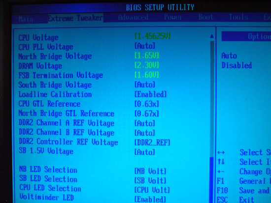
FSB Termination Voltage:
The scale runs from 1.2V-2V in .02V increments. Again, the board overvolts the BIOS setting by around 0.03V-0.04V. We recommend that users do not exceed a setting of 1.56V (1.6V actual) for 24/7 use. As FSB is raised with a quad-core CPU, VTT also needs to be raised. Expect to use between 1.5V-1.6V for overclocks past 440 FSB.
CPU GTL Reference:
Available options are, 0.57x, 0.59x, 0.61x, and 0.63x. This function controls GTL reference voltage to both CPU die's simultaneously. This is not completely ideal as there are always mismatches in CPU fabrication and motherboard components that may require individual GTL voltage level adjustments for each CPU die. The only option of use here is 0.63x, which is actually mislabeled and closer to around 66-67% of VTT. Intel specification for GTL reference voltages is 67%. We probed the on-board voltages with a DMM to find out just how close ASUS is to the 67% mark of VTT.
| Voltage Investigations | ||||
| BIOS Set VTT | Measured VTT | BIOS set GTL | Measured GTL | 67% of VTT |
| 1.50 | 1.53 | 0.63x | 1.022 | 1.025 |
| 1.52 | 1.55 | 0.63x | 1.036 | 1.038 |
| 1.54 | 1.57 | 0.63x | 1.051 | 1.051 |
| 1.56 | 1.60 | 0.63x | 1.065 | 1.072 |
| 1.58 | 1.62 | 0.63x | 1.080 | 1.085 |
| 1.60 | 1.64 | 0.63x | 1.090 | 1.098 |
The closest point to 67% on our motherboard for both CPU die is 1.54V (set in BIOS). Although the differences between actual GTL and Intel 67% specification seem small, fine control of the GTL voltages would have helped the board's overall stability when pushing past 450FSB with the Quad Cores. Each board will have a different level of voltage variance due to on-board component tolerances. In short, a 0.63x setting for GTL at 1.54VTT will not equate to the same measured GTL value on every board and may be adrift from the ideal 67% specification.
NB GTL Reference:
The scale runs from 0.49x to 0.67x in 0.02X increments. 0.67% worked best on our board and processors. We found that values lower than 0.67x caused lock ups and non-boot situations. Again, finer control options would have been nice and should be expected on a board in this price range.
We listed our BIOS settings below for a stable 450FSB run of the Prime95 torture test (8 hours 54mins passed), for those who are interested in this type of stability. Please note that component abilities do vary from board to board; these settings are only an approximate guideline.
| 450FSB Quad-Core BIOS Settings | |
| CPU Feature | |
| Ai Overclock Tuner | [Manual] |
| OC From CPU Level Up | [Auto] |
| CPU Ratio Control | [Manual] |
| Ratio CMOS Setting: | [8] |
| FSB Frequency | [450] |
| FSB Strap to North Bridge | [400MHz] |
| PCIE Frequency | [110] |
| DRAM Settings | |
| DRAM Frequency | [DDR2-1199MHZ] |
| DRAM Command Rate | [2T] |
| DRAM Timing Control | [Manual] |
| CAS# Latency | [5] |
| RAS# to CAS Delay | [5] |
| RAS# Precharge | [5] |
| RAS# Active Time | [12] |
| RAS# To Ras# Delay | [3] |
| Row Refresh Cycle Time | [42] |
| Write Recovery Time | [6] |
| Read To Precharge Time | [3] |
| Read To Write Delay(S/D) | [8] |
| Write To Read Delay(S) | [3] |
| Write To Read Delay(D) | [5] |
| Read To Read Delay(S) | [4] |
| Read To Read Delay(D) | [6] |
| Write To Write Delay(S) | [4] |
| Write To Write Delay(D) | [6] |
| DRAM Static Read Control | [Disabled] |
| Ai Clock Twister | [Strong] |
| Transaction Booster | [Enabled] |
| Boost Level | [0] |
| Voltage Settings | |
| CPU Voltage | [1.43125v] |
| CPU PLL Voltage | [Auto] |
| North Bridge Voltage | [1.61v] |
| DRAM Voltage | [2.16v] |
| FSB Termination Voltage | [1.54v] |
| South Bridge Voltage | [Auto] |
| Loadline Calibration | [Enabled] |
| CPU GTL Reference | [0.63x] |
| North Bridge GTL Reference | [0.67x] |
| DDR2 Channel A REF Voltage | [Auto] |
| DDR2 Channel B REF Voltage | [Auto] |
| DDR2 Controller REF Voltage | [DDR2_REF] |
| SB 1.5V Voltage | [Auto] |
| . | |
Conclusion
The term "underwhelming" was used by us in our introduction to describe our sentiments about the X38 in DDR2 configurations. After testing the ASUS Maximus Formula SE for the past few weeks, the initial memory latency and bandwidth figures had us feeling exactly that way too. Of course, recent BIOS updates have improved the situation and once we broke past the synthetic memory benchmarks, it became clear that real world gaming or application usage does not suffer at all from the apparent synthetic deficit at equivalent processor speeds. We did find this board to be very quick and certainly worthy of attention for those looking to build a premium gaming platform or for the enthusiast looking to get the most out of their processor while utilizing DDR2 memory technology.
The lack of memory divider options to really push the board seems to be an issue from Intel's end, as the Gigabyte/MSI/Foxconn/abit X38 motherboards suffer the same malady. For DDR2 users, the decision of which chipset to buy can be summed up by considering whether or not you intend to run two graphics cards in Crossfire mode or do not plan on upgrading to Penryn shortly. For single GPU systems, we think a sub $175 P35 motherboard like the abit IP35 Pro is an excellent purchase while tweakaholics will have the superlative DFI LP UT P35 T2R, fulfilling the upper-end enthusiast role. However, considering the quickly maturing BIOS releases and the additional performance gains that come with them, we are no longer adverse to recommending an X38 DDR2 board. If we had to make a choice today, the ASUS Maximus Formula SE would be at the top of our X38 DDR2 list.
So, apart from running Crossfire in dual x16 mode and having a fairly tweakable BIOS, where does this leave the ASUS Maximus Formula? On the plus side, the latest BIOS releases are maturing rapidly, and we have found no real incompatibility issues using XP or Vista with a wide variety of components. Though the BIOS is touted as being for the "Extreme Tweaker", it's very easy to use. There are a few quirks to auto overclocking with the 0505 BIOS, voltages tend to drift towards the high side, at times outside the realms of safety in our opinion. This is why we suggest using manual settings as the best overclocking option for long term use. The bios recovery system worked flawlessly after a failed overclock setting and continues to be the best in the industry. We also found the features available on the board and the component choices utilized are excellent for the most part.
Our biggest gripes revolve around the somewhat disappointing execution of the supplied water block design and unreliable 1/2" tubing clamps when using high flow rate pumps. Sure, we love the concept - a single water block cooling two key areas of the motherboard, saving a lot of user cost and PC case clutter. Unfortunately, the bonding of the block to the Northbridge heatsink makes the whole water-cooling concept almost meaningless with our particular board sample. In non-modified form, the differences between running air rather than water to cool the Northbridge are virtually nonexistent. We have passed our suggestions to ASUS, who seem very willing to explore ways of improving the current design. Given the choice of spending in excess of $70 for two good water blocks to cover the Northbridge, and Southbridge, we prefer a well-implemented single block solution from ASUS. We have expressed our concerns to ASUS and they have shipped us a new board to test that hopefully resolves this problem.
We want ASUS to continue supplying their easy to use BIOS tweaking functions for mass audiences, though we feel that they do not need to combine "tweaker" functions under a respun marketing slogan. The current inclusion of a very limited and coarse GTL reference adjustment, "Transaction Booster", "Static Read Control" and "Clock Twister" actually prevents the enthusiast from full and flexible control, especially when the motherboard is pushed really hard (which it probably will be considering its target market). In this price class we need the option of full tweaking - certainly if a board is marketed as "Extreme Tweaker" as it should offer just that. ASUS definitely faces some stiff competition from Gigabyte, whose GA-X38-DQ6 offers nearly the same performance and features, bar the water-cooling out of the box. Then we have the possibility of DFI's and abit's X38 DDR2 offerings complicating choices even further. Oh, we also forgot the upcoming X48 chipset, which is bound to be more than just a speed binned X38 but is still targeted for the DDR3 performance crowd.
Extreme benchmarkers do make up a small percentage of the overall PC market, yet the success of an enthusiast level product hinges largely upon their opinion. The current buzzword in the benching scene is DDR3 and ASUS has its grip firmly on that market, with their DDR3 boards (Maximus/Formula Extreme) holding most of the Futuremark 3D world records. This leaves the appeal of current DDR2 X38 boards to early adopters who are either running CrossFire, waiting for a DDR3 price drop, or for Penryn to finally arrive. We have to acknowledge that the real test for supremacy between the X38 and P35 is yet to come - by that we are referring to the Penryn based processors that will be hitting retail shelves shortly. Once users have retail silicon on hand, it will be interesting to see how well both chipsets handle high FSB rates on the new processors. In our early testing, the nod goes to the X38 and is one more reason to consider the chipset once it matures. More than ever in this segment of the market, it's still all about features and overclocking. In this regard, we have to give the ASUS Maximus Formula SE a passing grade, and a recommended buy when looking at the current X38 offerings.


