Original Link: https://www.anandtech.com/show/2231
ATI Radeon HD 2900 XT: Calling a Spade a Spade
by Derek Wilson on May 14, 2007 12:04 PM EST- Posted in
- GPUs
While AMD will tell us that R600 is not late and hasn't been delayed, this is simply because they never actually set a public date from which to be delayed. We all know that AMD would rather have seen their hardware hit the streets at or around the time Vista launched, or better yet, alongside G80. But the fact is that AMD had quite a few problems in getting R600 out the door.
While we couldn't really get the whole story from anyone, we heard bits and pieces here and there during our three day briefing event in Tunis, Tunisia. These conversations were short and scattered and not the kind of thing that it's easy to get a straight answer about when asking direct questions. Keeping that in mind, we do have some information and speculation about a few of the road bumps AMD faced with R600.
Apparently, the first spin of R600 silicon could only communicate over the debugging interface. While the upside is that the chip wasn't totally dead, this is not a good problem to have. We also overheard that a later revision of the hardware suffered from fragments getting stuck in pixel shaders. We even overheard one conversation where someone jokingly remarked that AMD should design hardware but leave the execution to NVIDIA.
In a wild bout of pure speculation on our part, we would have to guess about one other problem that popped up during R600's creation. It seems to us that AMD was unable to get their MSAA hardware to work properly and was forced to use shader hardware to handle MSAA rather than go back for yet another silicon revision. Please know that this is not a confirmed fact, but just an educated guess.
In another unique move, there is no high end part in AMD's R600 lineup. The Radeon HD 2900 XT is the highest end graphics card in the lineup and it's priced at $399. While we appreciate AMD's intent to keep prices in check, the justification is what we have an issue with. According to AMD, it loses money on high end parts which is why we won't see anything more expensive than the 2900 XT this time around. The real story is that AMD would lose money on a high end part if it wasn't competitive, which is why we feel that there's nothing more expensive than the 2900 XT. It's not a huge deal because the number of people buying > $399 graphics cards is limited, but before we've started the review AMD is already giving up ground to NVIDIA, which isn't a good sign.
More than anything, we'd guess that the lack of a high end part has a lot to do with the delays and struggles AMD saw this time around in bringing R600 to market. We expect to see the return of a very high end part by the time R700 comes around, assuming that there aren't similarly debilitating delays.
The delays and lack of a high end would be beyond perfect if the Radeon HD 2900 XT could do to NVIDIA what the G80 launch did to ATI, unfortunately the picture just isn't that rosy. ATI's latest and greatest doesn't exactly deliver the best performance per watt, so while it doesn't compete performance-wise with the GeForce 8800 GTX it requires more power. An ultra high end power requirement in a sub-$400 graphics card isn't exactly ideal.
Despite all of this, there's a great deal of cool technology in the R600, and as ATI is now a part of a CPU company, we received more detail on the GPU than we've gotten during any other GPU launch. AMD takes graphics very seriously, and it recently reaffirmed its commitment to continue to deliver high end discrete graphics cards, so amidst countless delays and rumors of strange problems, the R600 architecture is quite possibly more important to AMD than the graphics cards themselves. An eventual derivative of this architecture will be used in AMD's Fusion processors, eventually making their way into a heterogeneous multi-core AMD microprocessor.
With AMD's disappointing Q1, it can't rest too much on the hope of Fusion changing the market, so we'll have to start by looking at where R600 is today and how it stacks up to NVIDIA's latest and almost greatest.
DX10 Redux
Being late to the game also means being late to DirectX 10; luckily for AMD there hasn't been much in the way of DX10 titles released nor will there be for a while - a couple titles should have at least some form of DX10 support in the next month or two, but that's about it. What does DX10 offer above and beyond DX9 that makes this move so critical? We looked at DirectX 10 in great detail when NVIDIA released G80, but we'll give you a quick recap here as a reminder of what the new transistors in R600 are going to be used for.
From a pure performance standpoint, DX10 offers more efficient state and object management than DX9, resulting in less overhead from the API itself. There's more room to store data for use in shader programs, and this is largely responsible for the reduction in management overhead. For more complex shader programs, DX10 should perform better than DX9.
A hot topic these days in the CPU world is virtualization, and although it's not as much of a buzzword among GPU makers there's still a lot to talk about the big V when it comes to graphics. DirectX 10 and the new WDDM (Windows Display Driver Model) require that graphics hardware supports virtualization, the reason being that DX10 applications are no longer guaranteed exclusive access to the GPU. The GPU and its resources could be split between a 3D game and physics processing, or in the case of a truly virtualized software setup, multiple OSes could be vying for use of the GPU.
Virtual memory is also required by DX10, meaning that the GPU can now page data out to system memory if it runs out of memory on the graphics card. If managed properly and with good caching algorithms, virtualized graphics memory can allow game developers to use ridiculously large textures and objects. 3DLabs actually first introduced virtualized graphics memory on its P10 graphics processor back in 2002; Epic Games' Tim Sweeney had this to say about virtual memory for graphics cards back then:
"This is something Carmack and I have been pushing 3D card makers to implement for a very long time. Basically it enables us to use far more textures than we currently can. You won't see immediate improvements with current games, because games always avoid using more textures than fit in video memory, otherwise you get into texture swapping and performance becomes totally unacceptable. Virtual texturing makes swapping performance acceptable, because only the blocks of texels that are actually rendered are transferred to video memory, on demand.
Then video memory starts to look like a cache, and you can get away with less of it - typically you only need enough to hold the frame buffer, back buffer, and the blocks of texels that are rendered in the current scene, as opposed to all the textures in memory. So this should let IHVs include less video RAM without losing performance, and therefore faster RAM at less cost.
This does for rendering what virtual memory did for operating systems: it eliminates the hard-coded limitation on RAM (from the application's point of view.)"
Obviously the P10 was well ahead of its time as a gaming GPU, but now with DX10 requiring it, virtualized graphics memory is a dream come true for game developers and will bring even better looking games to DX10 GPUs down the line. Of course, with many GPUs now including 512MB or more RAM it may not be as critical a factor as before, at least until we start seeing games and systems that benefit from multiple Gigabytes of RAM.
Continuing on the holy quest of finding the perfect 3D graphics API, DX10 does away with the hardware capability bits that were present in DX9. All DX10 hardware must support the same features and furthermore, Microsoft will only allow DX10 shaders to be written in HLSL (High Level Shader Language). The hope is that the combination of eliminating cap bits and shader level assembly optimization will prevent any truly "bad" DX10 hardware/software from getting out there, similar to what happened in the NV30 days.
Although not specifically a requirement of DX10, Unified Shaders are a result of changes to the API. While DX9 called for different precision for vertex and pixel shaders, DX10 requires all shaders to use 32-bit precision, making the argument for unified shader hardware more appealing. With the same set of 32-bit execution hardware, you can now run pixel, vertex, and the new geometry shaders (also introduced in DX10). Unified shaders allow extracting greater efficiency out of the hardware, and although they aren't required by DX10 they are a welcome result now implemented by both major GPU makers.
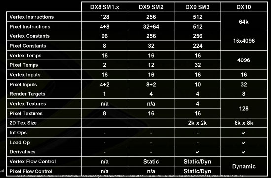
Finally, there are a number of enhancements to Shader Model 4.0 which simply allow for more robust shader programs and greater programmer flexibility. In the end, the move to DX10 is just as significant as prior DirectX revisions but don't expect this rate of improvement to continue. All indications point to future DX revisions slowing in their pace and scope. However, none of this matters to us today; with the R600 as AMD's first DX10 architecture, much has changed since the DX9 Radeon X1900 series.
R600 Overview
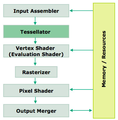
From a very high level, we have the same capabilities we saw in the G80, where each step in the pipeline runs on the same hardware. There are a lot of similarities when stepping way back, as the same goals need to be accomplished: data comes into the GPU, gets setup for processing, shader code runs on the data, and the result either heads back up for another pass through the shaders or moves on to be rendered out to the framebuffer.
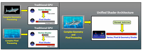
The obvious points are that R600 is a unified architecture that supports DX10. The set of requirements for DX10 are very firm this time around, so we won't see any variations in feature support on a basic level. AMD and NVIDIA are free to go beyond the DX10 spec, but these features might not be exposed through the Microsoft API without a little tweaking. AMD includes one such feature, a tessellator unit, which we'll talk about more later. For now, let's take a look at the overall layout of R600.
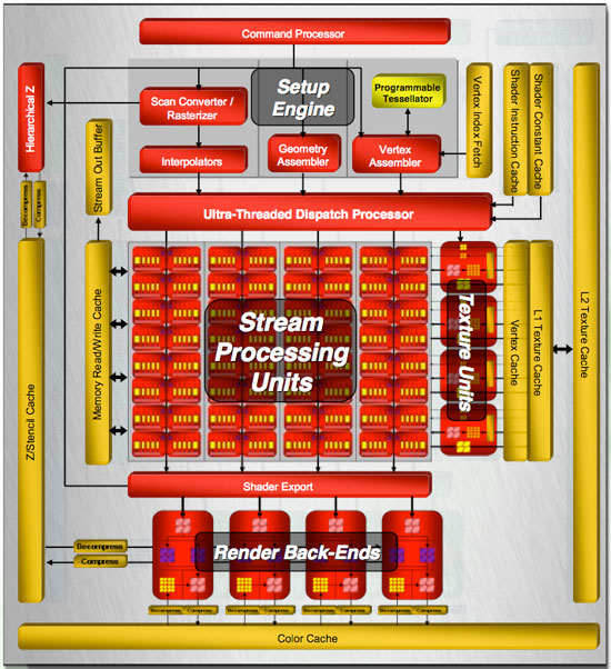
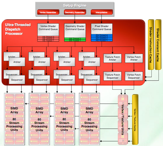
Our first look shows a huge amount of stream processing power: 320 SPs all told. These are a little different than NVIDIA's SPs, and over the next few pages we'll talk about why. Rather than a small number of SPs spread across eight groups, our block diagram shows R600 has a high number of SPs in each of four groups. Each of these four groups is connected to its own texture unit, while they share a connection to shader export hardware and a local read/write cache.
All of this is built on an 80nm TSMC process and uses in the neighborhood of 720 Million transistors. All other R6xx parts will be built on a 65nm processes with many fewer transistors, making them much smaller and more power efficient. Core clock speed is on the order of 740MHz for R600 with memory running at 825MHz.
Memory is slower this time around with higher bandwidth, as R600 implements a 512-bit memory bus. While we're speaking about memory, AMD has revised their Ring Bus architecture for this round, which we'll delve into later. Unfortunately we won't be able to really compare it to NVIDIA's implementation, as they won't go into any detail with us on internal memory buses.
And speaking of things NVIDIA won't go into detail on, AMD was good enough to share very low level details, including information on cache sizes and shader hardware implementation. We will be very happy to spend time talking about this, and hopefully AMD will inspire NVIDIA to start opening up a little more and going deeper into their underlying architecture.
To hit the other hot points, R600 does have some rather interesting unique features to back it up. Aside from including a tessellation unit, they have also included an audio processor on their hardware. This will accept audio streams and send them out over their DVI port through a special converter to integrate audio with a video stream over HDMI. This is unique, as current HDMI converters only work with video. AMD also included a programmable AA resolve feature that allows their driver team to create new ways of filtering subsample data.
R600 also features an independent DMA engine that can handle moving and managing all memory to and from the GPU, whether it's over the PCIe bus or local memory channels. This combined with huge amounts of memory bandwidth should really assist applications that require large amounts of data. With DX10 supporting up to 8k x 8k textures, we are very interested in seeing these limits pushed in future games.
That's enough of a general description to whet your appetite: let's dig down under the surface and find out what makes this thing tick.
Different Types of Stream Processors
The first thing we need to do when looking at the R600 shader core is to define our terms. AMD and NVIDIA build and refer to their Stream Processors (SPs) differently, and that makes counting them a little more difficult. Throughout our explanation, it will help to remember from our G80 coverage that threads refer to a vertex, primitive or pixel and not a stream of instructions as it would on a CPU.
Stream Processors: The NVIDIA Way
G80 has 128 SPs (for the 8800 GTX; there are 96 SPs on the 8800 GTS models) that are capable of doing a very small number of things at the same time. They can do either standard FP operations (like a MADD), a special function operation (like sine), or an integer operation. There are some cases where they can squeeze out an extra MUL, but more often than not this MUL isn't accessible. Each of these SPs operates on an individual thread (be it a vertex, primitive or pixel).
This gives us a total of up to 128 threads being processed per clock. It is important to realize that each of the 128 SPs isn't entirely independent. That is, we can't run 128 different instructions in one clock, in spite of the fact that we can run a number of instructions on 128 different threads. We'll delve a little deeper into this shortly, but depending on the type of shader running, the same instruction must be running on multiple threads.
For NVIDIA hardware, the minimum number of threads that must be processed using the same instruction is 16 (for vertex threads). NVIDIA's block diagrams show that each group of 16 SPs shares texture, register, and cache resources, so this makes sense. Pixel shaders, which are more important from a performance perspective, must run one instruction on 32 pixels at a time. What we can extrapolate from this is that NVIDIA can issue up to eight separate instructions across all of its 128 SPs (only four if working on pixels) per clock.
128 SPs / 16 Threads per Instruction per Clock = 8 Vertex Instructions per Clock
128 SPs / 32 Threads per Instruction per Clock = 4 Pixel Instructions per Clock
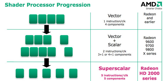
Stream Processors: AMD's R600
Things are a little different on R600. AMD tells us that there are 320 SPs, but these aren't directly comparable to G80's 128. First of all, most of the SPs are simpler and aren't capable of special function operations. For every block of five SPs, only one can handle either a special function operation or a regular floating point operation. The special function SP is also the only one able to handle integer multiply, while other SPs can perform simpler integer operations.
This isn't a huge deal because straight floating point MAD and MUL performance is by far the limiting factors in shader performance today. The big difference comes in the fact that AMD only executes one thread (vertex, primitive or pixel) across a group of five SPs.
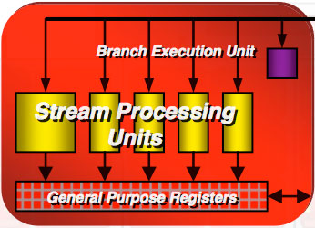
What this means is that each of the five SPs in a block must run instructions from one thread. While AMD can run up to five scalar instructions from that thread in parallel, these instructions must be completely independent from one another. This can place a heavy burden on AMD's compiler to extract parallel operations from shader code. While AMD has gone to great lengths to make sure every block of five SPs is always busy, it's much harder to ensure that every SP within each block is always busy.
If we take a step back, we can determine how many threads AMD is able to work on per clock. With 320 total SPs, each grouped into blocks of five-to-a-thread, we get 64 threads per clock. And here's where it starts to get complicated. Before we go back and compare this to NVIDIA's architecture, let's go a little deeper into the implementation.
Stream Processor Implementation
Going Deeper: Single Instruction, Multiple Data
SIMD (single instruction, multiple data) is the concept of running one instruction across lots of data. This is fundamental in the implementation of graphics hardware: multiple vertices, primitives, or pixels will need to have the same shader program run on them. Building hardware to do one operation at a time on massive amounts of data makes processing each piece of data very efficient.
In SIMD hardware, multiple processing units are tied together. The hardware issues one instruction to the SIMD hardware and all the processing units perform that operation on unique data. All graphics hardware is built on this concept at some level. Implementing hardware this way avoids the complexity of requiring each SP to manage not only the data coming through it, but the instructions it will be running as well.
Going Deeper: Very Long Instruction Word
Normally when we think about instructions on a processor, we think about a single operation, like Add or Multiply. But imagine if you wanted to run multiple instructions at once on a parallel array of hardware. You might come up with a technique similar to VLIW (Very Long Instruction Word), which allows you to take simple operations and, if they are not dependent on each other, stick them together as one instruction.
Imagine we have five processing units that operate in parallel. Utilizing this hardware would require us to issue independent instructions on each of the five units. This is hard to determine while code is running. VLIW allows us to take the determination of instruction dependence out of the hardware and put it in the complier. The compiler can then build a single instruction that consists of as much independent processing work as possible.
VLIW is a good way of exploiting parallelism without adding hardware complexity, but it can create a huge headache for compiler designers when dealing with dependencies. Luckily, graphics hardware lends itself well to this type of processing, but as shaders get more complex and interesting we might see more dependent instructions in practice.
Bringing it Back to the Hardware: AMD's R600
AMD implements their R600 shader core using four SIMD arrays. These SIMD arrays are issued 5-wide (6 with a branch) VLIW instructions. These VLIW instructions operate on 16 threads (vertices, primitives or pixels) at a time. In addition to all this, AMD interleaves two different VLIW instructions from different shaders in order to maximize pipeline utilization on the SIMD units. Our understanding is that this is in order to ensure that all the data from one VLIW instruction is available to a following dependent VLIW instruction in the same shader.
Based on this hardware, we can do a little math and see that R600 is capable of issuing up to four different VLIW instructions (up to 20 distinct shader operations), working on a total of 64 different threads. Each thread can have up to five different operations working on it as defined by the VLIW instruction running on the SIMD unit that is processing that specific thread.
For pixel processing, AMD assigns threads to SIMD units in 8x8 blocks (64 pixels) processed over multiple clocks. This is to enable a small branch granularity (each group of 64 pixels must follow the same code path), and it's large enough to exploit locality of reference in tightly packed pixels (in other words, pixels that are close together often need to load similar data/textures). There are apparently cases where branch granularity jumps to 128 pixels, but we don't have the data on when or why this happens yet.
If it seems like all this reads in a very complicated way, don't worry: it is complex. While AMD has gone to great lengths to build hardware that can efficiently handle parallel data, dependencies pose a problem to realizing peak performance. The compiler might not be able to extract five operations for every VLIW instruction. In the worst case scenario, we could effectively see only one SP per block operating with only four VLIW instructions being issued. This drops our potential operations per clock rate down from 320 at peak to only 64.
On the bright side, we will probably not see a shader program that causes R600 to run at its worst case performance. Because vertices and colors are still four components each, we will likely see utilization closer to peak in many common cases.
Next Up: NVIDIA's G80
NVIDIA has been more tight-lipped about their underlying architecture, but we will infer as much as possible from the block diagrams we've seen and conversations we've had.
The G80 shader core is a little different from the R600. It is built on eight SIMD units each containing 16 SPs. The SIMD instructions are not VLIW, but single scalar instructions, and each SP within a SIMD unit executes that instruction on a different thread. While groups of 16 SPs share resources, NVIDIA's compiler doesn't need to build VLIW instructions to schedule out any of these SPs and it would be quite difficult to create dependencies between SPs because they are running different threads.
The bottom line here is that up to eight distinct shader operations are running across 128 threads at one time. This means we could have 128 threads all complete a scalar operation every clock, or we could have 128 threads all complete a 4-wide vector operation one component at a time over four clocks.
On NVIDIA hardware, vertex threads are assigned to SIMD units in blocks of 16, while geometry and pixel threads are assigned in blocks of 32 (16 threads over two clocks). With smaller blocks, we see better branch performance but worse cache or prefetch utilization than we would with a more coarsely grained approach.
This implementation also means that we don't have to worry about dependencies in the shader code. Of course, it is also the case that we can't extract parallelism from the shader code itself. But the advantage gives us a steady rate of 128 operations per clock. This can actually go up in some special cases, but it shouldn't go lower under normal circumstances.
Comparing Shader Architectures: R600 vs. G80
The key to the architecture comparison is to realize that nothing is straight up apples to apples here. We need to look at how much work can be done per clock, how much work is likely to be done per clock, and how much work we can get done per unit time.
First, G80 can process more threads in parallel: 128 as opposed to R600's 64. Performing work on more threads at a time is one very good way of extracting overall parallelism from the problem of graphics. There are millions of pixels in every frame that need to be processed, and if we had hardware large enough we could process them all at once.
However, more work (up to 5x) is potentially getting done on each of those 64 threads than on NVIDIA's 128 threads. This is because R600 can execute up to five parallel operations per thread while NVIDIA hardware is only able to handle one operation at a time per SP (in most cases). But maximizing throughput on the AMD hardware will be much more difficult, and we won't always see peak performance from real code. On the best case level, R600 is able to do 2.5x the work of G80 per clock (320 operations on R600 and 128 on G80). Worst case for code dependency on both architectures gives the G80 a 2x advantage over R600 per clock (64 operations on R600 with 128 on G80).
The real difference is in where parallelism is extracted. Both architectures make use of the fact that threads are independent of each other by using multiple SIMD units. While NVIDIA focused on maximizing parallelism in this area of graphics, AMD decided to try to extract parallelism inside the instruction stream by using a VLIW approach. AMD's average case will be different depending on the code running, though so many operations are vector based, high utilization can generally be expected.
However, even if we expect high utilization on AMD hardware, the fact remains that G80 has a large clock speed advantage. With the shader core on G80 pushed up to 1.5 GHz, we could still see some cases where R600 is faster, but the majority of the time G80 should be able to best R600 on a pure compute basis.
This overview still isn't the bottom line in performance. Efficient latency hiding, good scheduling, high cache utilization, high availability of texture data, good branching, and fast and efficient Z/stencil and color processing all contribute as well. Where possible, let's explore those areas a bit more.
Texturing, Caches, and Memory
Texturing
R600 features less texture hardware than we would expect to see, though AMD stands by the argument that compute power will come out on top when it matters. At the same time, we can't compute anything if we don't have any data to work with. So let's take a look at what AMD has done with their texture units.
There are four texture units in R600, one for each SIMD unit. These units don't share resources with the hardware in the SIMD units and are independently scheduled by AMD's dispatch processor. The dispatch processor is able to determine what data will be needed for threads about to execute and can handle setting up the texture units without waiting for the SIMD unit to request data and come up empty.
Texture units on the R600 are able to make both filtered and unfiltered texture requests no matter what shader is running. Unfiltered textures are useful with non-image-based texture data like vertex textures, normal maps, and generic blocks of data. Filtered requests will generally be for image data to be used in determining the color of a pixel. R600 can address one unfiltered texture per clock per texture unit and one filtered textures per clock per texture unit. Filtered units can be used to request unfiltered textures if necessary, providing an extra four unfiltered textures in place of one filtered texture.
The unfiltered texture requests will come back through four fp32 texture samplers (one per component), while the filtered requests will return 16 data points which will be run through the texture filtering hardware resulting in four filtered texture samples. The hardware can at best produce 32 single component fp16 unfiltered results per texture unit per clock. More practically, each texture unit can produce four bilinear filtered four component fp16 samples per clock alongside four unfiltered results. For textures with fp32 components, two clocks would be required to complete a bilinear filter process, as only half the data is loaded at a time to conserve bandwidth.
This is definitely a step up for R600, as R5xx hardware doesn't have texture filtering hardware for floating point textures. All told, with each of its four texture units working, R600 can consume up to 32 unfiltered textures or 16 unfiltered textures plus 16 filtered textures (as long as they're fp16 or fewer bits and we're only using bilinear filtering).
G80 is built with four texture address units and eight texture filters per block of 16 SPs. In total, this means NVIDIA's hardware can produce 32 filtered texture samples per clock (again these are fp16 and bilinear filtered). Of course, NVIDIA is operating on twice as many threads per clock, so it is conceivable that they would benefit more from having the extra filtered data.
We will have to wait and see if AMD's approach of providing unfiltered and filtered texture access in parallel pays off. For the general case on pixel shaders, we would want to see more filtered textures per clock, but with vertex and geometry shaders coming into the mix this could be a good way to save hardware space while offering more texturing power. On a final texturing note, AMD implemented "percentage closer" filter hardware for depth stencil textures. This will allow developers to implement fast soft shadows. The details of the implementation weren't indicated though.
Finally: A Design House Talks Cache Size
We're quite used to talking about cache sizes on Intel and AMD CPUs, but graphics hardware has been another story. We've been asking for quite some time, while other sites have taken to writing shader code to come up with educated guesses about how much data fits on die. Today we are very happy to bring you everything you could ever want to know about R600 caches.
The four texture units are connected to memory through two levels of cache. Unfiltered texture requests go through the Vertex Cache (which is unfiltered) and filtered requests make use of the L1 Texture Cache. Each of these caches is 32kB read only. All texture units share these caches.
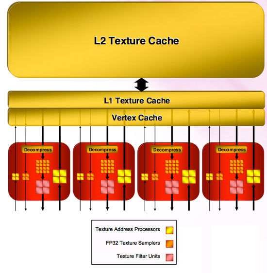
Both the L1 Texture Cache and the Vertex Cache are connected to an L2 cache that is 256kB. This is the largest cache on the chip, and will certainly handle quite a bit of data movement with the possibility of 8k x 8k texture sizes moving forward.
As for the shader hardware, the cache connected to the SIMD units is an 8 kB read / write cache. This cache is used to virtualize register space if necessary, export data to the stream out buffer (which can be done from any type of thread and can bypass the need to send data to the render back ends). This cache is also used to accelerate things like render to vertex buffer.
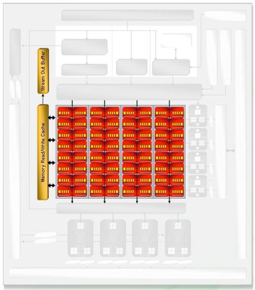
Most of R600's write caches are write-back caches, although we weren't given any specifics on which write caches are not write-back. The impression is that any unit that needs to write out over the memory bus is connected through a write cache that enables write combining to maximize bus utilization, write latency hiding, and short term reuse. We assume that the shader cache (what AMD calls the Memory Read/Write Cache) is also write-back.
The only thing we are really missing regarding caches is the information for Z/stencil cache and color cache connected off of the render back ends.
Memory and Data Movement
Internal cache bandwidth on the R600 is 180GB/sec, while the internal memory bus, a second generation Ring Bus that builds on the X1k series idea, is able to deliver 100GB/sec of throughput in either read or write capacity. Memory offers nearly 110GB/sec, and AMD has stated that the internal bus is well matched to this due to the fact that some external bandwidth is wasted on overhead. The bottom line here is that a whole of data can move very quickly into and out of this hardware.
As we mentioned, R600 sees a reincarnation of the Ring Bus which can now handle both read and write data (X1k could only handle reads on the Ring Bus while writes were run through a crossbar). An independent DMA controller manages a bus comprised of multiple ring stops. There is one ring stop per pair of memory channels, and each ring stop is connected to two others via a 256 bit wide connection. The ring bus is 1024 wires total and can move read and write data in either direction to follow the shortest path around the ring to or from the memory client or memory.
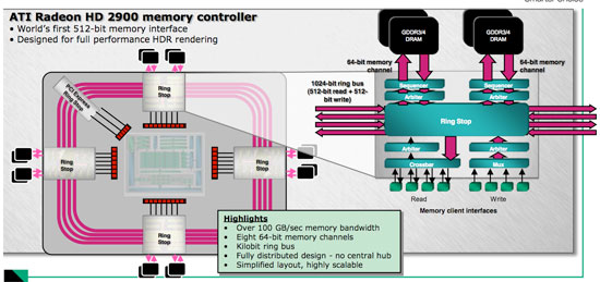
The Ring Bus allows the PCI Express bus to be treated like just another memory device by the rest of the hardware. The DMA hardware is able to manage all the traffic to and from onboard and system memory in the same manner, and the memory clients on the GPU don't need to know what device they're talking to. The Ring Bus services 84 read clients and 70 write clients.
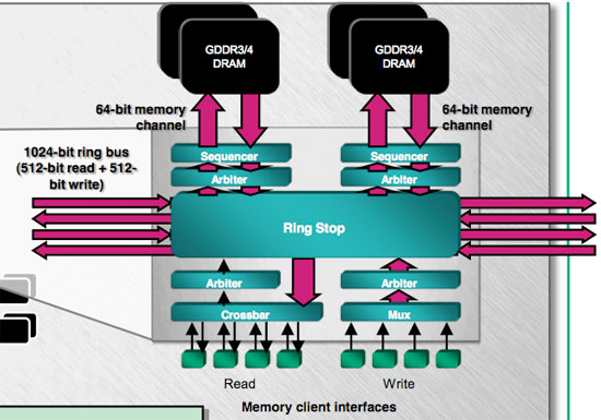
The external memory interface is 512-bit, doubling the X1k maximum of 256-bit and surpassing G80's 384-bit memory bus. Memory speeds are lower than on previous generation high end AMD hardware, but total bandwidth is higher. The net result is that AMD only slightly edges out G80 for memory bandwidth.
In implementing the 512-bit memory interface, AMD didn't want to add any more I/O pads to its package. They accomplished this by making use of a stacked I/O pad design. Unfortunately, details were vague on the implementation and methods used to keep clock speed high in spite of the proximity of other high frequency I/O.
Beyond the Shader: Coloring Pixels
We can't ignore the last few steps in the rendering pipeline, as AMD has also updated their render back ends (analogous to NVIDIA's ROPs) which are responsible for determining the visibility of each fragment and the final color of each pixel on the screen. Beyond this, the render back ends handle compression and decompression, render to texture functionality, MRTs, framebuffer formats, and usually AA.
Once again, one of the important things to note is that R600 only has four render back ends. This means we will only see 16 pixels complete per clock at maximum, just like the R580. However, AMD has included double the Z/stencil hardware so that we can get up to 32 total Z/stencil ops out of the render back ends to improve stencil shadow operations among other things. Pure fill rate hasn't really mattered in a while, while Z/stencil capability remains important. But will only four render back ends be enough?
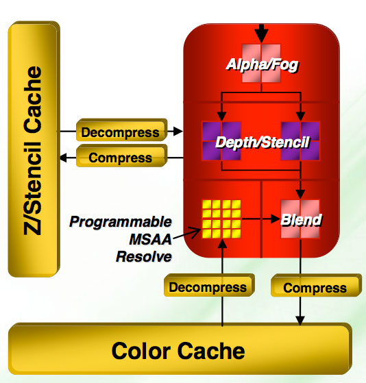
Efficiency has been improved on the render back ends, but with the potential of completing 64 threads per clock from the shader hardware, they will need to really work to keep up. R600 has the ability to display floating point formats from 11:11:10 up to 128-bit fp. DX10 requires eight MRTs now, and we've got them. We also get more efficient render to texture features which should help enable more complex effects to process faster.
Z/Stencil Hardware
As far as Z/stencil hardware is concerned, compression has gotten a boost up to 16:1 rather than 8:1 on the X1k series. Depth tests can be limited to a specific range programmatically which can speed up stencil shadows. Our Z-buffer is now 32-bit floating point rather than 24-bit. Hierarchical Z has been enhanced to handle some situations where it was unable to assist in rendering, and AMD has added a hierarchical stencil buffer as well.
AMD is introducing something called Re-Z which is designed to also help with the problem Early-Z has in not being able to handle shaders that update Z data. R600 is able to check Z values before a shader runs as well as after the Z value has been changed in the shader. This allows AMD to throw out pixels that are updated to be out of view without sending them to the render back ends for evaluation.
If we compare this setup with G80, we're not as worried as we are about texture capability. G80 can complete 24 pixels per clock (4 pixels per ROP with six ROPs). Like R600, G80 is capable of 2x Z-only performance with 48 Z/stencil operations per clock with AA enabled. When AA is disabled, the hardware is capable of 192 Z-only samples per clock. The ratio of running threads to ROPs is actually worse on G80 than on R600. At the same time, G80 does offer a higher overall fill rate based on potential pixels per clock and clock speed.
CFAA and No Fixed Resolve Hardware
That's right, R600 doesn't have hardware dedicated to resolving MSAA in the render back end - the only MSAA related tasks handled in the render back end are compression and evaluation of the subpixels. All antialiasing resolve is performed on the shader hardware. Certainly, AMD would prefer we start by telling you about the neat custom resolve filters that can be implemented on their shader hardware, but we would rather speculate about this for a moment first.
AMD has stated that, moving forward, in addition to allowing programmable sample patterns, future DX versions may allow for custom resolve filters as well. This is cited as one of the reasons why R600 uses shader hardware to resolve AA samples. AMD has given us a couple different resolve filters to play with, which we'll talk about in a minute. But at a point where we're seeing the first DX10 hardware from graphics makers, and at a time where competitive performance is paramount, it doesn't seem like the decision we would have made.
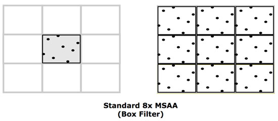
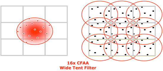
Whatever the circumstances, R600 sends its pixels back up from the render back ends to the shader hardware to combine subpixel data into a final pixel color. In addition to the traditional "box" filter (which uses subpixels within the area of a single pixel), the new driver offers the ability to use subpixel data from neighboring pixels resolved with a tent filter (where the impact of the subpixels on final color is weighted by distance). AMD calls this CFAA for custom filter antialiasing.
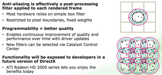
AMD currently offers narrow and wide tent filters which can be implemented using 2, 4, or 8 multisamples per pixel boundary. This gives us nine different AA options including traditional box filters. More filter options can be provided via driver updates, as these are essentially driver managed shader programs. Here's the breakdown of the options based on the type of filter and the number of samples used to resolve each pixel.
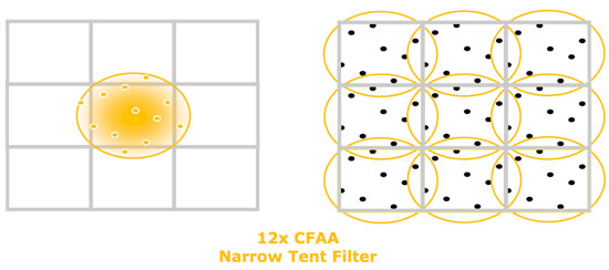
One of the useful side effects of these tent filters is that they are also capable of antialiasing interior pixels, not just those covered by more than one triangle. This is helpful in getting rid of aliasing in textures which can occur in certain cases.
While tent filters are a very interesting idea to improve antialiasing, they are not without their drawbacks. First, it is possible for tent filters, even though neighboring subpixel data is weighted less than internal subpixels, to create a muddy look, especially with high contrast fine detail like thin text for example. While tent filters can antialias textures on interior pixels, they can also create a blur effect where it isn't needed which removes detail from the scene.
Edge Detection
While tent filters are good in the general edge case, in order to be really compelling from an image quality stand point, AMD decided to go a step further and adaptively apply more AA in places where it would do the most good and less elsewhere. This will be done by applying an edge detect algorithm to the framebuffer and using more aggressive AA on these edges.
We learned that edge detection can be sped up by looking at pixel compression. If all the subpixels for one fragment are the same color, compression will be at its highest and there is no edge within that pixel. Beyond using this information, we are told that the algorithm uses straightforward derivative computations to find high frequency data (high contrast edges) much the same way Photoshop does.
The combination of edge detection and tent filters gives us two extra option beyond the ones listed above: 12x narrow tent filter with edge detect and 24x wide tent filter with edge detect. These filters are capable of very good image quality, though this quality does come at a performance cost. We will take a look at performance and image quality after we finish going through R600 hardware.
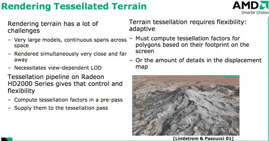
Tessellation and the Future
It's no secret that R600 is AMD's second generation unified shader architecture. The Xbox 360 houses their first attempt at a unified architecture, and the R600 evolved from this. It isn't surprising to learn that some of the non-traditional hardware from the Xenos (the Xbox 360 GPU) found its way into R600.
AMD has included a tessellator on their hardware, which is able to take input geometry and amplify it before passing it on to the vertex shader. This is something that Microsoft is planning on adding to future versions of DirectX as well, but in the meantime developers will need to take special steps to utilize the hardware.
The basic idea behind tessellation is in the subdivision of geometry. There are multiple algorithms for handling this process, and the R600 tessellator is capable of adapting to a developer's specific needs. The tessellator can take a polygon as input and break it up into smaller triangles, creating more vertices for a specific object. Taken on its own, this isn't particularly useful, but this concept can be paired with displacement mapping in order to reshape the tessellated polygon into something more like the actual surface a developer wants to represent (this is called the limit surface).
With low polygon models and lots of pixel shaders, normal maps and textures can approximate the look of more complex geometry, but we're always stuck with the very rough silhouette edge around the object. With more geometry, we could also better use pixel shaders to enhance the geometry present rather than trying to create the illusion of geometry itself.
We can't simply send millions of polygons per character to the graphics card. This isn't because the card can't handle the processing requirements, but rather the bandwidth and latency overhead of sending all this data to the hardware is too high. Tessellation and displacement gives us a way of really using the vertex shading power of unified architectures as well as removing the limitation on polygon count created by overhead.
While geometry shaders can be used for amplification and tessellators can be written as geometry shaders, this process is still way too slow on current programmable hardware. AMD's dedicated tessellator is capable of tessellating up to 15x more data and it can work much faster and more efficiently than a geometry shader set to the same task. With the next version of DX bringing tessellator hardware to all GPUs, developers should be able to focus on more interesting uses for the geometry shader as well.
Having this unit makes porting Xbox 360 games even easier for developers targeting AMD hardware. As most hardware still doesn't support the feature, a more general purpose path will still have to be written, but there wouldn't be any reason to remove what's already there. In these cases, R600 could benefit with greater performance than other hardware.
The downside is that it might be difficult to entice developers not already working with the Xbox 360 to touch the tessellator. It is definitely capable of high performance and terrific detail, but spending time on a feature only a small subset of gamers will be able to experience (for this generation) takes away from time spent making the game better for everyone.
We are always happy to see either hardware or software take a leap and create the first chicken or egg, but we just don't see the tessellator as a big selling point of R600. The technology is great, we're glad it's there, but we will really have to wait and see just how much (if any) real value this adds to the product. We'll leave this section on one final note about a tessellator landscape demo that really brings home what this thing can do.
The New Video Decode Pipeline: UVD
UPDATE: Since the launch of the HD 2900 XT, we've learned that all HD 2000 series parts except the high end R600 based parts will have UVD. This means that the HD 2900 XT will feature the same video decode acceleration offered on the R5xx hardware. As higher end cards are usually paired with faster CPUs, AMD feels that UVD on R600 is unnecessary.
This comes as a bit of a surprise to us and to certain board partners who's box art claims UVD as a feature of the HD 2900 XT. We do apologize for any confusion we may have caused at launch.
NVIDIA beat AMD to the punch with their full H.264 decode acceleration on G86/G84. Of course, AMD is one upping NVIDIA this time around, as their UVD (Unified Video Decode) architecture is also capable of decoding VLC bitstreams on all three HD media codecs. This means that there are no cases where AMD hardware will not handle 100% of the video decode process (after the CPU has dealt with pulling the encrypted content off the disk and preparing it to send to the GPU that is).
Here's a diagram of the landscape as it stands now. Notice that G80 is not capable of the bitstream decode or the inverse transformation (either iDCT or otherwise), but G84/G86 come very close to matching AMD's capabilities.
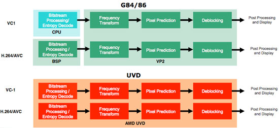
At the same time, we should remember that bitstream decode is only really heavy under H.264. Certainly VC-1 and MPEG-2 will see some benefit, but they are already fairly manageable. NVIDIA stated that building the hardware to handle VLC bitstreams wouldn't have a high enough return on investment. AMD, however, indicated that their bitstream processors are at least a little bit adaptable and it wasn't that difficult to include VLC decode.
Either way, the best way to figure out what's going on is to take a look at performance and see if there really is any advantage to R600 over G86. Unfortunately, try as we might, we could not get UVD to work with the current drivers provided by AMD and the PowerDVD release that is supposed to enable the hardware acceleration on HD 2000 series parts. We will have to take a second look at hardware decode when AMD and CyberLink or Intervideo get their software in order.
For now, our information leads us to believe that performance won't be hugely improved over G84/G86 in MPEG-2 and VC-1 CPU offloading. Where we might start to see a difference is in AMD's 65nm HD 2000 and mobility series parts. These have the potential to decrease power consumption by large amounts and provide quiet running systems for HTPCs, or longer battery life for notebooks. We will have to wait to get our hands on the higher volume R6xx based parts though. Also worth nothing is that AMD's high-end hardware does something that NVIDIA's 8800 series cards currently don't, so NVIDIA users that want fast H.264 decoding support are stuck with slower 3D performance.
AMD CFAA Performance and Image Quality
While we've already talked about CFAA, let's take a look at how it compares to other AA methods. We've already seen NVIDIA's CSAA in action, which is able to better determine how subsample colors should be weighted within a pixel. How does it stack up to AMD's tent filters? Let's take a look:

Zip file of uncropped JPG images (1.7MB)
Clearly CFAA does do a good job at reducing the impact of high contrast edges. As we mentioned before though, this doesn't come without drawbacks. Antialiasing shouldn't just filter out high frequency image data (which comes in the form of high contrast edges). The problem lies in the fact that some of these edges are supposed to be there.
Applying a blur to everything isn't the best general purpose answer. Ideally we want to balance eliminating high frequency data we don't want (aliased edges) while preserving the high frequency data we do want (fine grained detail in either geometry or interior textures). A balance needs to be kept here, and (as we've seen many times in the past) the answer for the end user can often be subjective.
This is certainly an interesting solution, but we will stick with simple 4x box filtered MSAA for our current and future tests as it still offers the best balance between image quality and performance - especially at very small pixel sizes. But before we leave the subject completely, let's take a look at how CFAA performs on R600. We'll compare it to all the non-transparent texture aware AA modes available on the X1950 XTX and 8800 GTS 640MB.
General Image Quality
Beyond antialiasing, there are quite a number of factors that go into making real-time 3D look good. Real-time graphics are an optimization problem, and the balance between performance and quality is very important. There is no single "right" way to do graphics, and AMD and NVIDIA must listen carefully to developers and consumers to deliver what they believe is the sweet spot between doing things fast and doing things accurately.
NVIDIA currently offers much more customizable image quality. Users are able to turn on and off different optimizations as they see fit. AMD really only offers a couple specific settings that affect image quality, while most of their optimizations are handled on a per game basis by the ominous feature known as Catalyst A.I. The options we have are disabled, standard and advanced. This doesn't really tell us what is going on behind the scenes, but we leave this setting on standard for all of our tests, as this is the default setting and most users will leave it alone.
Aside from optimizations, texture filtering plays a large role in image quality when high levels of filtering are called for. It's trivial to point sample or bilinear filter, and no one skimps on these duties, but when we get to trilinear and anisotropic filtering the number of texture samples we need and the number of calculations we must perform per pixel go up very quickly. In order to mitigate the cost of these operations, both AMD and NVIDIA attempt to apply high levels of filtering where they are needed and not-so-high levels of filtering where it won't matter that much. Of course there is much debate over where to draw the lines here, and NVIDIA and AMD both choose different paths.
To investigate texture filtering quality, we have employed the trusty D3D AF-Tester. This long-lived application enables us to look at one texture with different colored mipmap levels to see how hardware handles filtering them under different settings. Thankfully, we don't have to talk about angle dependent anisotropic filtering (which is actually a contradiction in terms anyway). AMD and NVIDIA both finally do good quality anisotropic filtering that results in higher resolutions textures being used more of the time where possible. Take a look at these images to see how the different hardware stacks up.
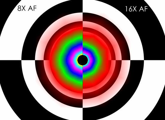
NVIDIA G80 Tunnel 8x/16x AF
G80
R5xx
R6xx
It still looks like NVIDIA is doing slightly more angle independence filtering. In practice, it will be very difficult to tell the difference between an image rendered on AMD hardware and one rendered on NVIDIA hardware. We can also see that AMD has slightly tweaked their AF technique to eliminate some of the odd transitions we noticed on R5xx hardware. This comes through a little better if we look at a flat plane:
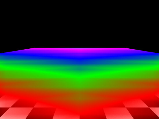
AMD R600 Plane 8x AF
R5xx
R6xx
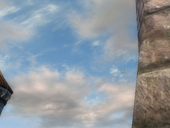
We did happen to notice at least one image quality issue not related to texture filtering on AMD hardware. The problem turns up in Rainbow Six: Vegas in the form of very bad banding where we should see HDR lighting. We didn't notice this problem on G80, as we can see from our comparison.
  |
| Click to enlarge |
We also noticed a small issue with Oblivion at one point where the oblivion gate shader would bleed through other objects, but this was not reproducible and we couldn't get a screenshot of it. This means it could be a game related issue rather than a hardware or driver problem. We'll keep our eyes peeled.
Overall IQ of the current DX10 hardware available is quite good, but we will continue to dig further into the matter to make sure that everything stays that way. We're also waiting for DX10 games before we can determine if there are other differences, but hopefully that won't be the case as DX10 has a single set of requirements.
The AMD HD 2000 Series Lineup
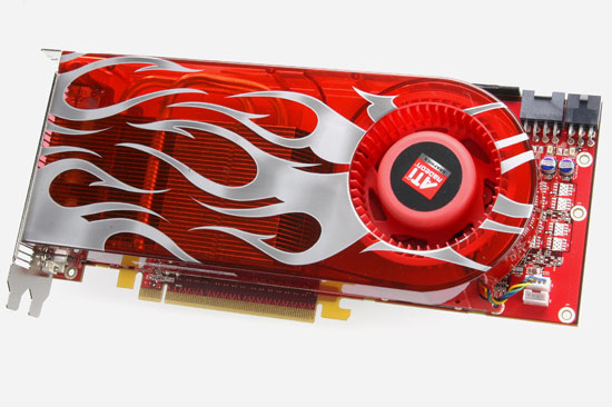
The announcement today includes a top-to-bottom lineup of DX10 class hardware including four mobile parts (with one additional DX9 mobile part sharing the HD 2000 series naming) and five desktop parts. While all of this hardware is being made public, we've only got one piece of hardware to bring to the table today: the R600 based Radeon HD 2900 XT.
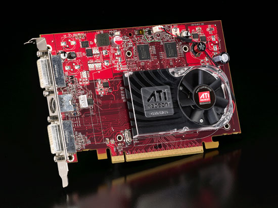
Performance on all other R6xx parts won't be available until "late June", but we can still talk about what these parts will be when they finally make it to market. On the desktop, in addition to the HD 2900 XT, we will see the Radeon HD 2400 Pro and XT in the "value" segment, with the HD 2600 Pro and XT providing good mainstream-to-midrange gaming performance.
ATI Radeon HD 2600 XT
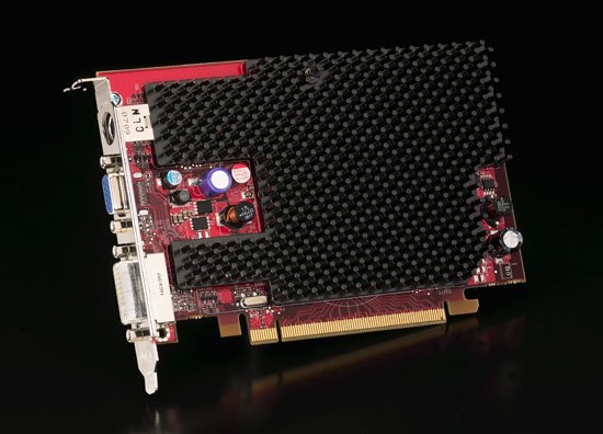
ATI Radeon HD 2400 XT
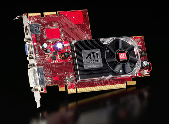
ATI Radeon HD 2400 Pro
There is currently no add-in retail hardware planned that tops the HD 2900 XT, but we are hearing rumors that faster parts may be available through OEMs only. This is unconfirmed at present, so take it with a grain of salt. Let's take a look at a break down of what we do know we'll be getting:
| AMD R6xx Hardware | ||||||||
| SPs | RBEs | Core Clock | TMUs | DDR Rate | Bus Width | Memory Size | Price | |
| HD 2900 XT | 320 | 16 | 740MHz | 16 | 825MHz | 512bit | 512MB | $399 |
| HD 2600 | 120 | 4 | 600 - 800MHz | 8 | 400 - 1100MHz | 128bit | 256MB | $99 - $199 |
| HD 2400 | 40 | 4 | 525 - 700MHz | 4 | 400 - 800MHz | 64bit | 128MB / 256MB | <$99 |
It's harder to pin down all the specs of the mobile parts, as all the clock speeds (and sometimes bus width) can change depending on the TDP envelope a notebook maker is working with. While we aren't certain, our best guess is that mobile parts named similarly to desktop parts will have the same internal configuration of SPs, texture units, and render back ends. The exception here is the Mobility Radeon HD 2300, which is a DX9 part based on R5xx hardware.
While 2400 and 2600 standard and XT versions will exist in the mobile space, there are currently no plans for a high end mobile part. This is very likely due to the high power draw and low performance per watt we see with AMD's 80nm R600. We don't expect to see a higher performance mobile part until AMD can get the power consumption of its higher end hardware down (likely with a process shrink).
Just for comparison, let's take a look at what NVIDIA is currently offering as well. Here's a table of all the G8x based parts on the market.
| NVIDIA G8x Hardware | ||||||||
| SPs | ROPs | Core Clock | Shader Clock | DDR Rate | Bus Width | Memory Size | Price | |
| 8800 Ultra | 128 | 24 | 612MHz | 1.5GHz | 2.16GHz | 384bit | 768MB | $830+ |
| 8800 GTX | 128 | 24 | 576MHz | 1.35GHz | 1.8GHz | 384bit | 768MB | $600 - $650 |
| 8800 GTS | 96 | 20 | 513MHz | 1.19GHz | 1.6GHz | 320bit | 640MB | $400 - $450 |
| 8800 GTS 320MB | 96 | 20 | 513MHz | 1.19GHz | 1.6GHz | 320bit | 320MB | $300 - $350 |
| 8600 GTS | 32 | 8 | 675MHz | 1.45GHz | 2GHz | 128bit | 256MB | $200 - $230 |
| 8600 GT | 32 | 8 | 540MHz | 1.19GHz | 1.4GHz | 128bit | 256MB | $150 - $160 |
| 8500 GT | 16 | 4 | 450MHz | 900MHz | 800MHz | 128bit | 256MB / 512MB | $89 - $129 |
Sapphire's HD 2900 XT
We wanted to include some noise and overclocking performance here as well, but we don't like testing overclocking with reference or engineering samples, as they don't always reflect what we'll see on store shelves. We've got a better chance of seeing real world characteristics in boards from specific vendors.
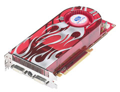 Sapphire went to a lot of trouble to get us a board, but due to a shipping mishap we were unable to test it in time for this review. Later this week we'll take a follow-up look at R600 including overclocking and Vista performance to fill in the gaps we weren't able to cover here. We really appreciate Sapphire's efforts to help us get this coverage into our launch article, but we'll have to wait on this data.
From what we see with our engineering samples, core clock speeds of 850MHz+ are possible, but whether this will have a large impact on performance remains to be seen. We will also be working hard on getting a roundup of retail hardware out as soon as possible including overclocking, power, heat, noise, and all the other fun stuff that makes a big difference in retail hardware.
 And we won't just see a bunch of cookie cutter retail designs out there either. Sapphire and others will have custom cooled and factory overclocked boards on their way as soon as possible. Even though AMD won't have the highest performing part on the market, or even a pretender to the throne, we can see a great competitor to the 8800 GTS emerge if prices and clock speeds from retail partners hit the mark.
Power Supply Requirements
With new product launches, we expect to see increased power requirements for increased performance. With the 8800 series, we saw hardware that offered excellent performance without breaking the bank on power, while the highest end part available required two PCIe power connectors. We can forgive the power gluttony of the 8800 GTX as the 8800 GTS offers terrific performance with a more efficient use of power.
R600 goes in another direction. We have a new part that doesn't compete with the high end hardware but has even more stringent power requirements. While NVIDIA's $400 hardware offered good power efficiency, AMD's Radeon HD 2900 XT eats power for breakfast. In fact, with the R600, we see the first use of PCIe 2.0 power connectors. These expand on the current 6-pin power connector to offer up to 150W over an 8-pin configuration.
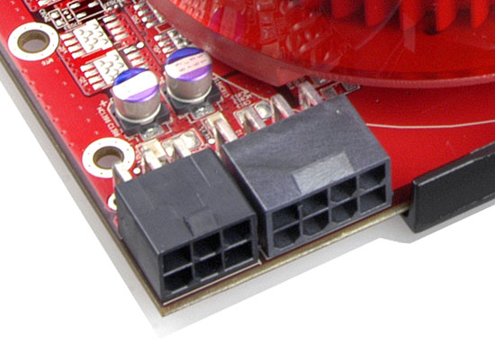
The 8-pin PCIe 2.0 power connector enables graphics cards to pull up to 300W of power just for themselves. With 75W delivered through the slot, 75W through a 6-pin PCIe power cable, and 150W sliding down the PCIe 2.0 wire, the R600 has plenty of juice on tap. While it doesn't pull a full 300W in any test we ran, overdrive won't be able to function without the combination of a 6-pin and 8-pin connector.
All is not lost, however, as two 6-pin connectors will still be able to power the R600 for normal operation. The 8-pin receptacle will accept a 6-pin cable leaving two holes empty. This doesn't degrade performance when running R600 at normal clock speeds, but overclocking will be affected without the added power.
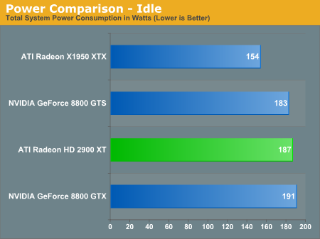
The bottom line as we'll shortly show is that AMD has built hardware with the performance of an 8800 GTS in a power envelope beyond the 8800 Ultra. We will take a closer look in our performance benchmarks when we actually test power draw under idle and load using 3dmark06.
The Test
| CPU: | Intel Core 2 Extreme X6800 (2.93GHz/4MB) |
| Motherboard: | EVGA nForce 680i SLI ASUS P5W-DH |
| Chipset: | NVIDIA nForce 680i SLI Intel 975X |
| Chipset Drivers: | Intel 8.2.0.1014 NVIDIA nForce 9.53 |
| Hard Disk: | Seagate 7200.7 160GB SATA |
| Memory: | Corsair XMS2 DDR2-800 4-4-4-12 (1GB x 2) |
| Video Card: | Various |
| Video Drivers: | ATI Catalyst 8.37 NVIDIA ForceWare 158.22 |
| Desktop Resolution: | 2560 x 1600 - 32-bit @ 60Hz |
| OS: | Windows XP Professional SP2 |
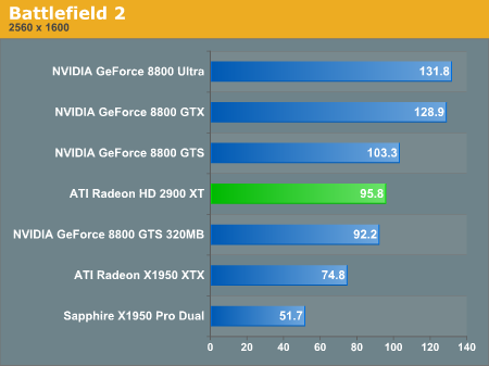
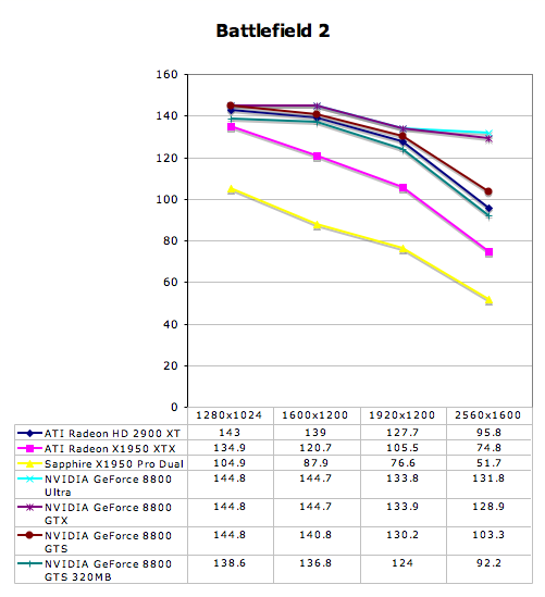
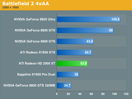
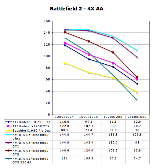
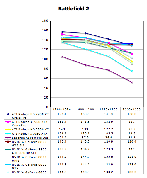
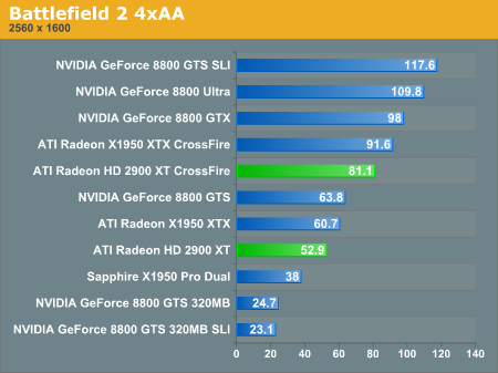
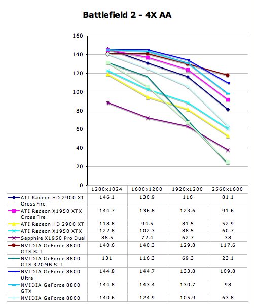
Battlefield 2 Performance
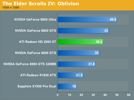
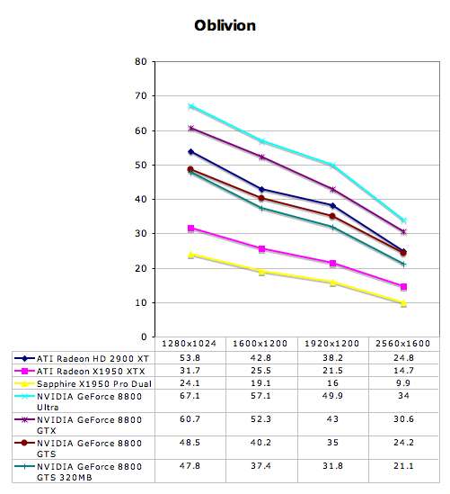
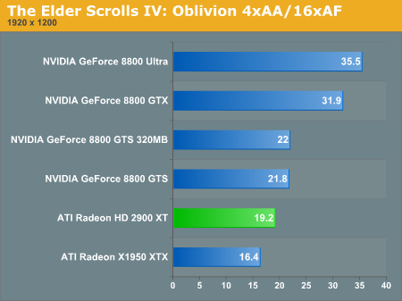
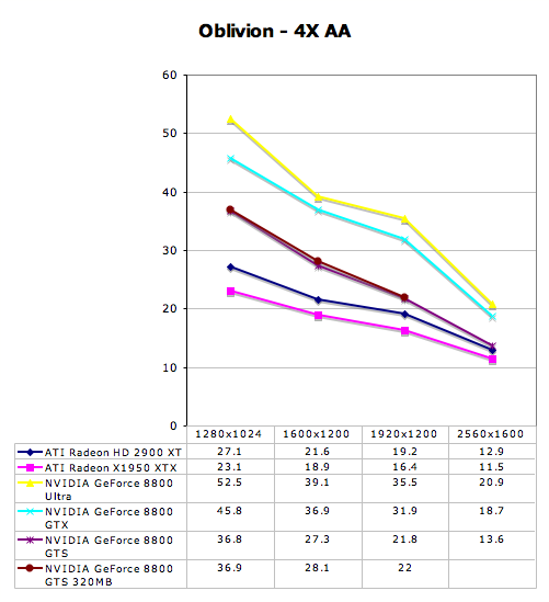
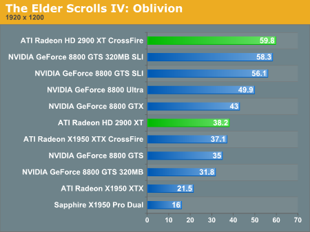
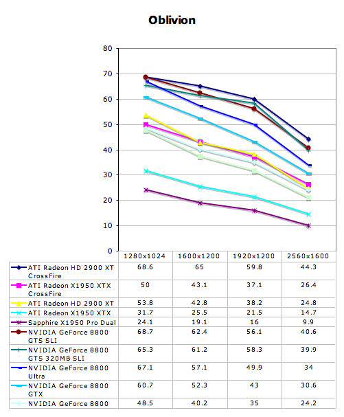
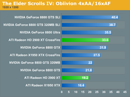
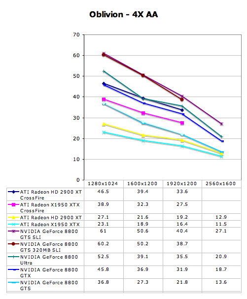
The Elder Scrolls IV: Oblivion Performance
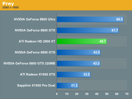
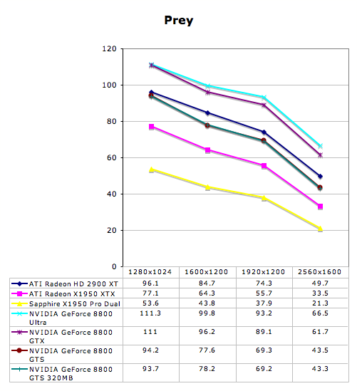
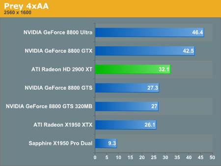
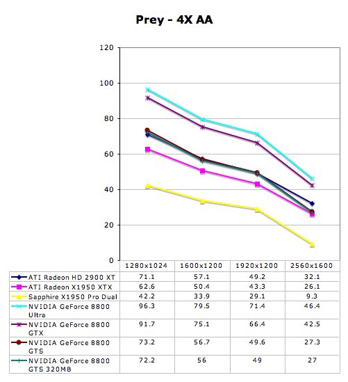
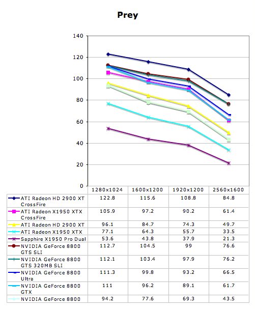
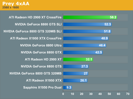
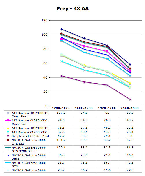
Prey Performance
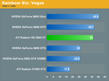
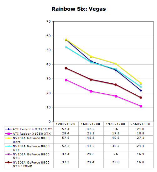
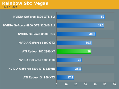
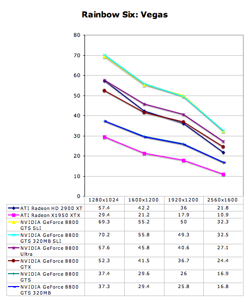
Rainbow Six: Vegas Performance
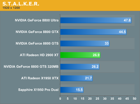
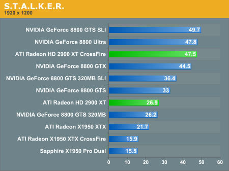
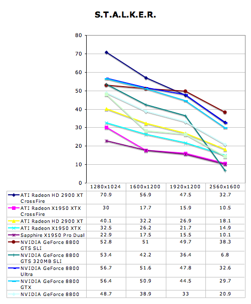
S.T.A.L.K.E.R. Performance
Supreme Commander Performance
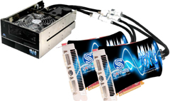
Multi-GPU Performance - Battlefield 2
Multi-GPU Performance - The Elder Scrolls IV: Oblivion
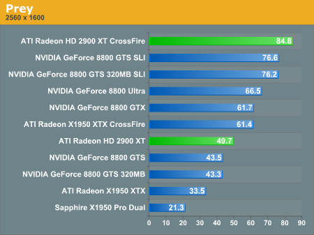
Multi-GPU Performance - Prey
Multi-GPU Performance - Rainbow Six: Vegas
Multi-GPU Performance - S.T.A.L.K.E.R.
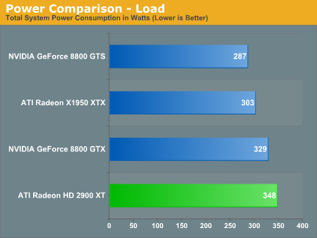
Power Performance
Power efficiency is where the Radeon HD 2900 XT really falls short; while performance is similar to NVIDIA's 8800 GTS, power consumption is significantly greater. The 2900 XT draws even more power than the 8800 GTX under load:
Final Words
What a long, strange journey it has been to this point. We have a very delayed launch from AMD that features a part that consumes quite a bit of power and doesn't compete with the competition's high end offering. At face value, this sounds quite a bit like NVIDIA's NV30 launch, but thankfully we wouldn't go so far as to call this NV30 Part 2: the R600 Story.
Even though AMD has not built a high end part, they have built a part that runs very consistently at its performance target (which could not be said about NV30). AMD is also not trying to pass this card off as something it's not: rather than price this card out of its class, the R600 will find a good home at a reasonable price.
Despite the delays, despite the quirks, and despite the lack of performance leadership, AMD has built a good part. It might not be as exciting as an ultra high end card, and it certainly isn't as power efficient as an 8800 GTX or Ultra, but it has quite a few positives that make it an interesting product, and more competition is always a good thing. The worst thing that could happen now is for NVIDIA to get as complacent as ATI did after R300 wiped the floor with the competition.
Let's break it down with something akin to a pro/con list. Here's what AMD did right:
R600 features a tessellator which offers an interesting option to geeks and game developers even if it doesn't offer a lot of value to the average consumer. We've got full HD video decode acceleration for all the major codecs. There is a huge amount of processing power available for the code and data that fits the structure of the hardware. Audio is integrated into the video stream and sent out over HDMI with a special adapter allowing both DVI and HDMI to coexist and without the need of splitting the audio channel out from elsewhere. We like to see more options for antialiasing, and even if we don't necessarily like the tent filters the edge detect AA is a really cool concept that looks pretty good. And we absolutely love the architectural detail AMD has gone into with R600.
And here's what AMD did wrong:
First, they refuse to call a spade a spade: this part was absolutely delayed, and it works better to admit this rather than making excuses. Forcing MSAA resolve to run on the shader hardware is less than desirable and degrades both pixel throughput and shader horsepower as opposed to implementing dedicated resolve hardware in the render back ends. Not being able to follow through with high end hardware will hurt in more than just in lost margins. The thirst for wattage that the R600 displays is not what we'd like to see from an architecture that is supposed to be about efficiency. Finally, attempting to extract a high instruction level parallelism using a VLIW design when something much simpler could exploit the huge amount of thread level parallelism inherent in graphics was not the right move.
Maybe that's a lot to digest, but the bottom line is that R600 is not perfect nor is it a failure. The HD 2900 XT competes well with the 640MB 8800 GTS, though the 8800 GTS 320MB does have a price/performance advantage over both in all but the highest resolutions and AA settings under most current games. There are features we like about the hardware and we would love to see exploited. There is potential there, especially for Xbox 360 ports, to really shine... though console ports are often looked down upon in the PC market, particularly if they come late and offer little new to the platform.
Another bit question is that we still haven't seen how either G80 or R600 handle DX10 based games. This unknown will continue for just a little while longer, as next month we should start seeing some titles support DX10. The first titles may not be representative of later DX10 titles, however, so this is something we will only be able to properly assess with time.
For now, R600 is a good starting place for AMD's DX10 initiative, and with a bit of evolution to their unified shader hardware it could eventually rise to the top. We aren't as excited about this hardware as we were about G80, and there are some drawbacks to AMD's implementation, but we certainly won't count them out of the fight. Power efficiency on 65nm remains to be seen, and there is currently a huge performance gap NVIDIA has left between the 8600 GTS and the 8800 GTS 320MB. If AMD is able to capitalize here with the HD 2600 series, they will certainly still have a leg to stand on. We will have to wait to see those performance results though.
In the meantime, we are just happy that R600 is finally here after such a long wait. Let's hope for AMD's sake that the next revision of their hardware doesn't take quite so long to surface and manages to compete better with six month old competing products. We certainly hope we won't see a repeat of the R600 launch when Barcelona and Agena take on Core 2 Duo/Quad in a few months....


