Original Link: https://www.anandtech.com/show/2018
Introduction & Manufacturing
AMD held its spring Analyst Day on Thursday, and we were able to sit down and enjoy the webcast. While we fully expected to learn about AMD's next CPU architecture, K8L, we were pleasantly surprised to find a few unexpected extras. The event covered a huge swath of the computing industry in a manner that went just deep enough to leave us screaming for more. Unfortunately, we don't have all the answers we wanted today, but we do have some good ideas about what we'll be seeing in the near future about AMD's upcoming technology.
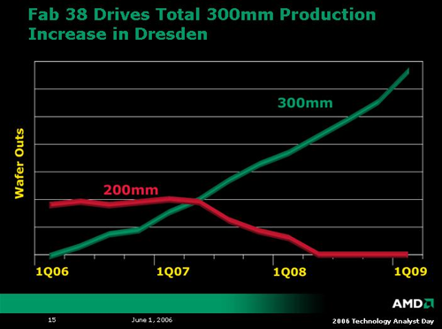
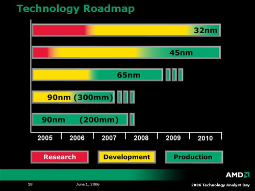
As could be expected, the day started off with an overview of AMD's fabrication strategies. In the near term, AMD is transitioning from 200mm wafers for its 90nm SOI process to 300mm wafers. This will help serve to get AMD up to speed with 300mm wafer before volume production of 65nm devices begins. As 200mm wafer production is phased out, 65nm processes will be ramping into full swing. AMD plans on an aggressive schedule for transitioning to the smaller process technology, and an even more aggressive schedule for pushing out 45nm technology after this product cycle. As of now, AMD plans to introduce production 45nm silicon only 18 months after 65nm hardware hits the market.
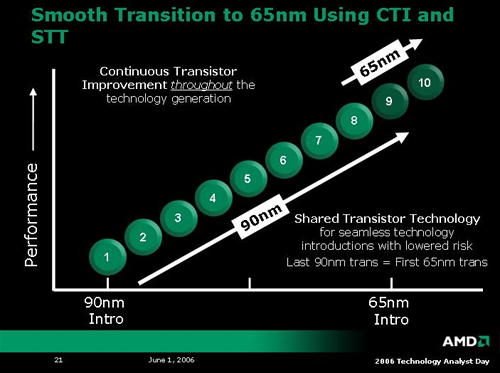
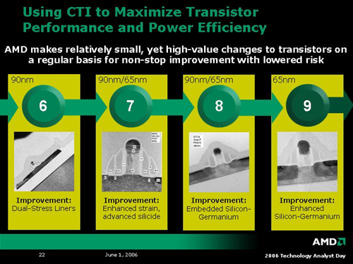
In moving to 65nm, AMD has adopted a strategy of constant improvement of its current transistor technology to ensure a smooth transition. The last generation 90nm parts will overlap the first generation 65nm parts, as many of the key features of their structures will be shared. AMD calls this Shared Transistor Technology and Continuous Transistor Improvement. As small improvements are made over the entire life cycle of a process, the final transition from one type of process to another is made much easier.
After AMD showed off a bunch of slides about how their fab is better than your fab, they started to touch on a few topics that really get our groove on: platform architecture. AMD introduced three new platform initiatives, and talked a little bit about their K8L architecture. First we'll talk about the direction AMD is moving with their platform technology.
Platform Strategy: 4x4, Torrenza, Trinity, and Raiden
It wouldn't be fair to completely ignore AMD Live!, as there was a fair amount of time spent talking about it. Unfortunately, AMD Live! is much like Intel's VIIV. That is to say, the "technology" is more of a suggestion about what components to include in computers built for a specific purpose in order to assist in the marketing of an idea. Certainly, the "computer as media center" idea isn't something new. Intel and AMD simply enabled the magic co-branding fairy to make end users feel all warm and squishy inside about their purchase. To be fair, mindshare is a large part of the game, and Centrino has served Intel very well on the mobile front (though I wish this early Centrino I've got had been a Pentium-M with onboard 802.11g).
Moving on, there were some very high powered (as in power draw) announcements. First off, AMD is pushing a new high end enthusiast platform consisting of dual socket motherboards for dual core processors combined with quad GPU solutions. In an incredibly unoriginal moment of indiscretion, this platform has been dubbed 4x4. Uninspired, yet very appropriate: the platform will very likely be large, loud, and so power hungry we will need a gas powered generator to run it. That doesn't mean we wouldn't want to own a system. We just aren't sure we'd want to pay for it.
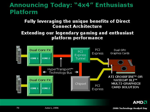
So, the first question we asked about 4x4 was: how much different is this than taking an off the shelf 2P board and dropping in a couple 2xx series Opteron processors with NVIDIA's quad SLI? Unfortunately, we haven't gotten any answer other than to say that there is something that makes it different. From what we understand, 4x4 will support unbuffered DIMMS (while Opterons still require registered memory), and the platform will be focused towards tweakable motherboards. We are looking into all the details. While the more power! kick is always interesting, we have to wonder if there will be any software in the near term that can really harness all this raw potential.
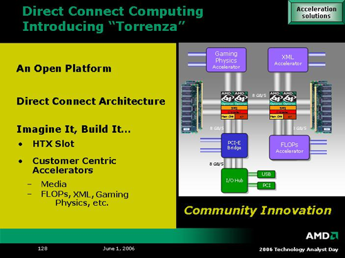
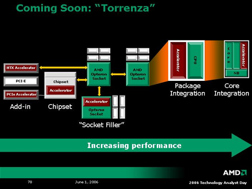
Stepping past the enthusiast platform, we have arguably the most exciting announcement of the day: Torrenza. Along with K8L, AMD plans on openly licensing it's (until now proprietary) coherent HyperTransport technology. At first glance, this may not seem exciting, but AMD is throwing in a little twist: HTX slots. These HTX slots will be standard interfaces connected directly to an AMD CPU's HyperTransport link. If both of these links are coherent, the device and the CPU will be able to communicate directly with each other with cache coherency. Because of this, latency can be reduced greatly over other buses as well, enabling hardware vendors to begin to create true coprocessor technology once again.
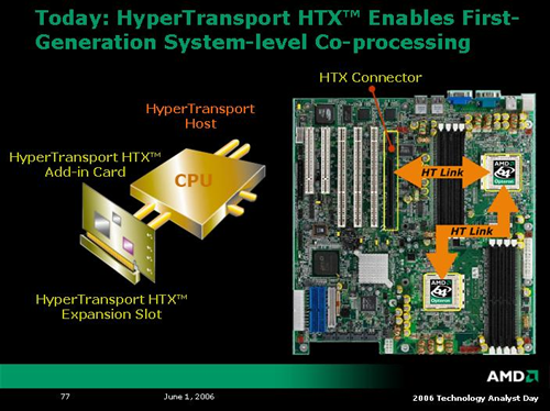
In addition to the flexibility of allowing the addition of such "accelerators" (as AMD calls them) to be added in via HTX slots, the architecture of the K8L line will be flexible enough that AMD could choose to incorporate some of these coprocessor technologies on a CPU package, or even on a CPU die itself. This is possible because the interconnect interface is the same at any level of integration. Not only will companies be able to develop their own unique solutions to extend the capabilities of the system processor, but it may even be possible to see such technology integrated into future AMD parts at a more fundamental level.
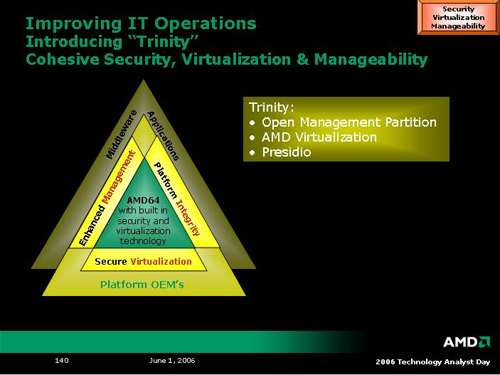
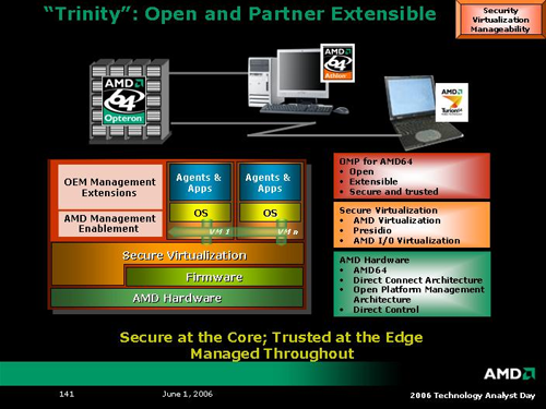
The next two platform level technologies AMD spoke on are named Trinity and Raiden. At many levels, Raiden seems more like an AMD Live! style initiative enabled by Trinity and other technologies, but we're getting ahead of ourselves. At its core, Trinity is AMD's platform level support for hardware virtualization. In addition to previously introduced Pacifica technology, AMD is working with the PCISIG to develop advanced I/O virtualization in addition to enhancing security and manageability of virtualized hardware at every level. The actual hardware that will enable Trinity wasn't explicitly expounded upon, but we did get these two slides with a brief description of how security, manageability and virtualization can't be handled as three separate problems.
Moving on to Raiden, AMD wishes to change the way businesses look at the way they provide computing to their employees. Rather than hardware, AMD believes businesses would be better served by focusing on compute cycles. Server and PC hardware can be setup in blade-like configurations, and employees can run thin clients which stream their OS from the compute server. Ideally, the reality of where their "compute power" comes from won't be important to the end user as long as there was no difference in experience. Having a large number of under utilized computers is a cost companies could avoid by sharing the processing power of fewer machines over a large number of people.
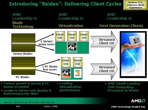
If there is any technology that is Raiden specific, AMD was not forthcoming. From what we can tell, AMD will leverage the current enthusiasm over blade systems and its Trinity virtualization platform to push customers toward a centralized computational model on the basis of power and cost savings. Certainly the benefits are there if the technology can support it, and hopefully we will be able to get some clarification on how Raiden translates to actual hardware.
K8L Architecture
At the outset, we hoped we'd have a very large section on AMD's new architecture. After our whirlwind of a three hour briefing, we aren't that much further along on the K8L architecture front than we were before. We've had some things confirmed by a few slides, but AMD didn't spend much time on these details. Over the next few days we will be sitting down with AMD and gathering as much detailed information about K8L as we can, but for now we can offer an overview of what we already know and have gathered from the slides we've seen.
The first K8L chips will be fabbed on a 65nm SOI process jointly developed by IBM and AMD, and manufactured at AMD facilities in Dresden. AMD has implemented a more modular approach to designing their next gen CPUs this time around in order to more easily meet the demands of a market craving ever increasing support for multicore technology. While CPUs are traditionally very hand tuned and designed on a low level, it appears AMD has taken an extremely object oriented approach to CPU design. The interfaces between different parts of the CPU are very strongly defined and it is possible for AMD to mix and match components as necessary.
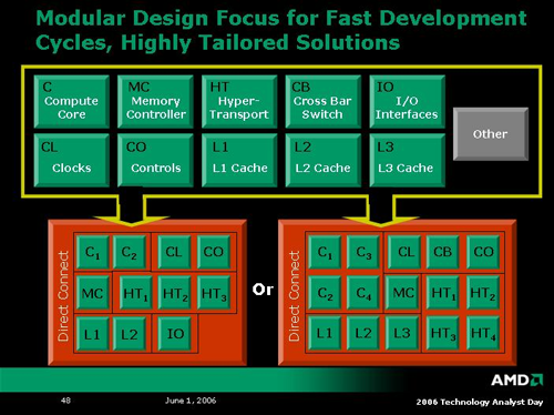
This type of approach makes a lot of sense in today's world. Designing processors without the need to reengineer the entire CPU from the ground up in order to add another compute core, HT link or (maybe) another memory controller is a stroke of brilliance. Dual and quad core systems don't need 2 or four of everything, but needs do change depending on the application targeted by the hardware. Hopefully AMD will use this technology to enable the delivery of changing CPU configurations much the same way we see clock speeds and cache sizes change over time today.
On a very slightly lower level architecture side, we have a slide showing the overview of AMD's next server class processor with 4 cores based on K8L. Features include a shared L3 cache, "enhanced IPC" cores, OoO (Out of Order) loads, wider data paths, HT-3 (the third version of HyperTransport), and support for DDR2 (and DDR3 or FBDIMMS in the future). Details on some of these enhancements were way too light, especially on the IPC (Instructions Per Clock) front.
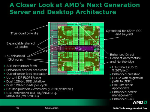
Cache enhancements include the capability to support 2x128-bit loads per cycle from the 64k L1 cache (which is half the size of the K8 L1 cache), and a shared L3 cache which will scale up from its introduction at 2MB. The shared L3 cache will help with features like node interleaving on multiprocessor systems as well as multithreaded apps which make use of shared data. We are still waiting for more detailed data on the cache architecture. It isn't clear whether the caches are all exclusive, and we would like to know more about associativity as well.
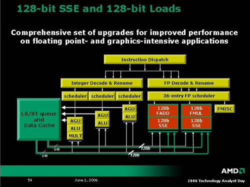
At a lower level, we have a block diagram of the compute core for K8L CPUs. Again, this diagram is a bit oversimplified, but we can see a few key features of the architecture. On the FP side, the CPU is able to handle 2x128-bit floating point or SSE operations per clock. While this isn't quite as flexible as Intel's Core with its 3 SSE units, AMD's K8L will be able to handle 4 double precision floating point operations per clock. . (Current K8 chips can only do 1x128/2x64-bit SSE instructions per clock.)
As with K8, K8L will have 3 ALUs (arithmetic logic units) and 3 AGUs (address generation units). Combined with cache enhancements and the new ability to reorder loads, K8L has a shot at outpacing Core in integer performance. Of course, we do still need more detail in this area to understand fully what's going on. No doubt, if AMD is claiming the ability to reorder loads, they can absolutely move loads ahead of loads (as this is the easiest case to handle). Where things get interesting is in the ability to move loads ahead of stores. Intel's Core architecture features some very interesting prediction technology in determining whether or not to move a load before a store. We haven't received an answer from AMD on whether they will tackle moving loads ahead of stores at all, let alone how they will handle memory disambiguation and/or prediction. In the past, we've seen a kind of "simpler is better" approach from AMD, so it will be interesting to see which direction K8L has taken.
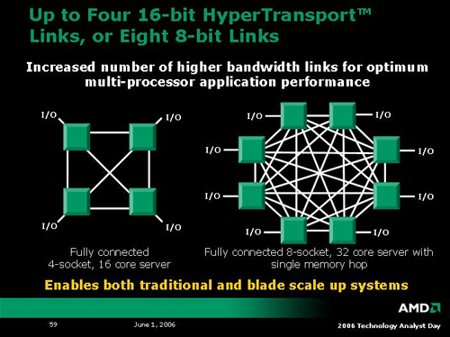
When it comes to processor interconnect technology, AMD has led Intel since the introduction of the Opteron. With K8L comes a very interesting enhancement to the interconnect architecture: each of the four 16-bit HyperTransport links can be split into two 8-bit HyperTransport links. Apparently, each of the resulting eight 8-bit HT links will be coherent and will allow a direct connection to another processor. In large systems, this means direct access from one core to seven others plus I/O, resulting in the possibility of fully connected 8-way systems. In a quad core world, that would be 32 cores on one platform. AMD also indicates that these HT connections can be used to easily scale blade implementations as well.
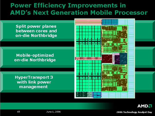
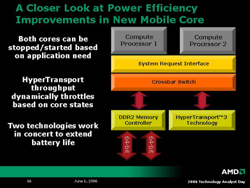
AMD mobile processors will also benefit from enhancements to HyperTransport with link power management. Not only will the new dual core 65nm K8L Turion processors be able to throttle cores independently, but even the HT links can be powered down when not in use. These enhancements will go a long way towards expanding AMD's mobile capabilities, especially if the K8L architecture can deliver better performance per Watt than the K8 before it. Compared to NetBurst architectures, K8 may as well have been an icebox, but that all changed with the introduction of Banias, Dothan, Yonah and now Core technology. Intel is bringing the fight to AMD, and K8L will need to deliver on the power front in order to remain competitive. The only market segment that really throws power to the wind is the extreme enthusiast (to which AMD's 4x4 initiative will certainly cater), but volume business will require an eye to the efficient.
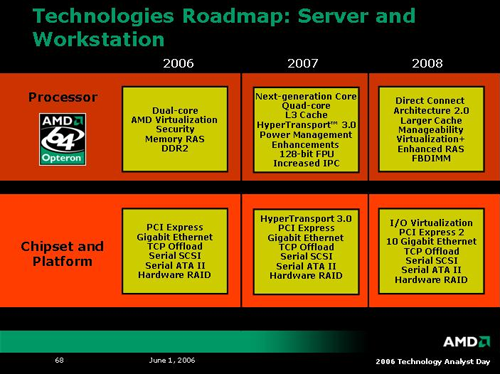
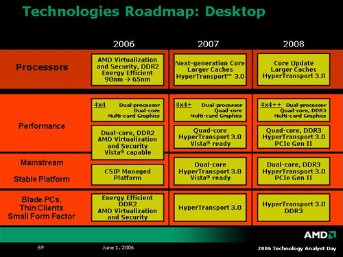
To round out what we learned about K8L architecture, here are the roadmap slides of technology AMD plans to roll out over the next three years.
Final Words
While AMD touched on an incredibly vast amount of technology and data over the course of their 3 hour webcast, the depth of each branch was not nearly enough to satisfy our tastes. We are in the process of scheduling briefings with as many AMD engineers as possible in order to get our questions answered, and we will certainly report on the details of our research as soon as we are able. Hopefully next week's Computex will be very fruitful on the AMD front.
We can't be too upset over the lack of detail though. In fact, for a day designed around presenting technology to analysts, AMD was pretty heavy on the technology and architecture. Now that they've officially confirmed some of the key features of their next gen processor and platform technology, we certainly hope they will be able to back up their claims with real architectural data on the hardware.
In the meantime, we can all dream sweet dreams over the possibilities AMD's Torrenza presents. Giving expansion cards the bandwidth and low latency of an HTX connection with the ability to support coherent HyperTransport will enable hardware vendors to create a new class of expansion card. Though AMD likes to call these "accelerators," we'll try our best to steer clear of buzz words and marketing speak. Suffice it to say that giving hardware vendors the capability of accessing any CPU or memory in the system directly with cache coherency should really shake things up. The advantages are probably most apparent to the HPC market, where HTX can offer an easy and standard way to add custom FPGAs or very specialized hardware to a massive system. However, there are absolutely advantages out there for those who want to build hardware to really work in lock-step with the CPU.
This applies directly to companies like AGEIA with their PhysX card which, when used in a game, must communicate bi-directionally with the CPU before a frame can be sent to the GPU for rendering. Additionally, GPU makers could easily take advantage of this technology to tie the graphics card even more tightly to the CPU and system memory. In fact, this would serve to eliminate one of the largest differences between PCs and game consoles. The major advantage that still remains on console systems (aside from their limited need for backwards compatibility compared to the PC) is the distance from the CPU to the GPU. There is huge bandwidth and low latency between these two subsystems in a console, and many games are written to take advantage of (or even depend on) the ability to actively share the rendering workload between the CPU and GPU on a very low level. Won't it be ironic if we start seeing high performance Xbox 360 and PS3 emulators only a couple years after their release? This is the kind of thing that could make it possible.
With Torrenza and the introduction of 4x4 in the consumer space, it seems clear that AMD will be offering consumer level CPUs with multiple external coherent HyperTransport channels. As the lack thereof has been the only limitation keeping us from building multiple processor systems with consumer products, we have to wonder how AMD will really differentiate its server and workstation parts this time around. Out of the gate, the K8L Opteron will be a 4 core part, while the desktop chip will only have 2, but eventually the desktop will support 4 cores as well. Will we start to see more specialized hardware "accelerators" on Opteron chips, or will we see more I/O oriented modules? Will HT-3's link unganging to allow 2 8bit links for every 16bit link only be available on the high end parts? AMD's leadership in performance in the 2P and 4P workstation market has been very solid since the beginning of Opteron, and we are excited to see the ways AMD will attempt to continue this trend.
The final word on AMD's Analyst Day? Performance. It's pure and simple, and AMD is all about it. On the high end it's 4x4 or 8 coherent HT links, and on the mobile side, its performance per Watt. By 2008, AMD hopes that 1/3 of the market place will let the world know that they've still got solid performance for the mainstream at good prices as well. The next gen CPU market will certainly be exciting to watch.


