Original Link: https://www.anandtech.com/show/1998
Introduction
Wide Dynamic Execution, Advanced Digital Media Boost, Smart Memory Access and Advanced Smart Cache; those are the technologies that according to the marketing people at Intel enable Intel to build the high performance, low energy CPUs using the new Core architecture.Of course, as an AnandTech Reader, you couldn't care less about which Hyper Super Advanced Label the marketing folks glue on their CPUs. "Extend the digital lifestyle by combining robust performance with low power consumption" could have been another marketing claim for the new Core architecture, but VIA already cornered that sentence for its C7 CPUs. The marketing slogans for Intel's Core and VIA's C7 are almost the same; the architectures are however vastly different.
No, let us find out what is really behind all this marketing hyper-talk, and preferably compare it with the AMD "K8" (Athlon 64, Opteron) architecture of Intel's NetBurst and Pentium M processors. That is what this article is all about. We talked to Jack Doweck, the engineer who designed the completely new Memory Reorder Buffer and Memory disambiguation system. Jack Doweck is one of the Intel Israel Development Center (IDC) architects.
The Intel "P8"
Intel marketing states that Core is a blend of P-M techniques and NetBurst architecture. However, Core is clearly a descendant of the Pentium Pro, or the P6 architecture. It is very hard to find anything "Pentium 4" or "NetBurst" in the Core architecture. While talking to Jack Doweck, it became clear that only the prefetching was inspired by experiences with the Pentium 4. Everything else is an evolution of "Yonah" (Core Duo), which was itself an improvement of Dothan and Banias. Those CPUs inherited the bus of the Pentium 4, but are still clearly children of the hugely successful P6 architecture. In a sense, you could call Core the "P8" architecture, with Banias/Dothan being based on the "P7" architecture. (Note that the architecture of Banias/Dothan was never given an official name, so we will refer to it as "P-M" for simplicity's sake.)Of course this doesn't mean that Intel's engineers just bolted a few functional units and a few decoders on Yonah and called it a day. Jack told us that Woodcrest/Conroe/Merom are indeed based on Yonah, but that almost 80% of both the architecture and circuit design had to be redone.
CPU architecture in a nutshell
For those of you who are not so familiar with CPUs, we'll start with a crash course in CPU architectures. To understand CPU design, you must first look at the instructions that are sent to the CPU, and thus we start with the software.Typical x86 software code consists of about 50% stores and loads, and there are about twice as many loads as there are stores. Of the remainder, about 15 to 20% of the instructions are branches (If, Then, Else), and the rest are mostly "ADD" (addition) and "MUL" (multiply) instructions. Only a very small percentage of code consists of more exotic instructions such as DIV (divisions), SQRT (square root), or other higher order math (e.g. trigonometric functions).
All these instructions are processed in a typical "Von Neuman" pipeline: Fetch, Decode, Operand Fetch, Execute, Retire.
Instructions are fetched based on the instruction pointer register, and initially they are nothing but long bit patterns to the CPU. It's only after the CPU starts decoding the bits that the instructions "start to make sense" to the CPU. Addresses and opcodes are decoded out of the instructions, and the addresses are used for the next step: the operand fetch. As you don't want the CPU to perform calculations with the addresses but rather on the content of these addresses - the "operands" - the CPU has to fetch the right data out of the data cache. Once these operands are put in the registers, the ALU is steered by the "opcode" (which has been decoded) to perform the right calculation on the operands in the registers.
The results are written to the architecture register file, the registers which can be used by the compiler. The results must also be written to the caches and the main memory, so that these are also up to date. That is the final phase, the retire phase. That is the basically how processing works in all CPUs.
The main challenge for the CPU designer today is the average memory latency the CPU sees. A Pentium 4 3.6 GHz with DDR-400 runs no less than 18 times faster than the base clock of the RAM (200 MHz). Every cycle the memory is being accessed, a minimum of 18 cycles pass on the CPU. At the same time, it takes several cycles to even send a request, and it takes a few cycles to send a request back. (We discussed this in the past in our overview of memory technology article.) The result is that wait times of 200 to 300 cycles are not uncommon on the Pentium 4. The goal of CPU cache is to avoid accessing RAM, but even if the CPU only has to go to system memory 4% of the time, that 4% of the time can lower performance significantly.
Smarter Prefetching and Caching
Making sure that the right instructions and data are ready for use in the caches in the "3 GHz and beyond" era is one of the most important tasks of the architectural engineer. This helps to ensure performance increases as clockspeeds get pushed higher; otherwise, higher CPU clockspeeds will simply result in the processor spending more time waiting for data. This technique of priming the caches is knows as Prefetching; however, the current hardware prefetching algorithms don't always lead to success. There are quite a few cases where they can actually lower performance, especially in bandwidth sensitive applications.The Core architecture prefetching is without any doubt superior to what can be found in the Athlon 64 and Pentium 4. There are no less than three prefetchers - two data, one instruction - in each core, plus two prefetchers for the L2-cache. With eight prefetchers active in one dual-core Core CPU, all those prefetchers could easily get in the way of the "demand" bandwidth - the bandwidth which is needed by the load operations of the running program. In order to avoid this bottleneck, the prefetch monitor of the Core CPUs always give priority to the demand bandwidth; the prefetchers will never steal too much bandwidth away from the running program.
There is more. The data prefetch needs to perform tag lookups (tags = index of cache) in the caches frequently. To avoid this resulting in higher latency for the "normal" (caused by the program running) tag lookups, the data prefetch uses the store port for the tag lookup. If you remember, loads happen about twice as often as stores. This means the store port is used only half as much as the load port and it make sense to use that port for tag lookup by the prefetchers. Note also that stores are not critical for system performance in most cases -- once the data is "written" the processor can go on about its business. The cache/memory subsystem is in charge of replicating the data down to main memory, and as long as this happens eventually, everything works fine.
The cache system of the Core CPU is also very impressive. A massive 4 MB L2-cache is shared between the two cores and is accessed in only 12 to 14 cycles. Each core also has a 3 cycle 32 KB Instruction cache and a 32 KB data cache at its disposal. Note that the "Trace Cache" of NetBurst has been left behind with the return to shorter pipelines; the NetBurst Trace Cache basically functions as an instruction cache for pre-decoded instructions, and while this was apparently helpful for the long pipeline of NetBurst, Intel has apparently determined that a traditional L1 caching scheme makes more sense for Core.
Cache Architecture Overview
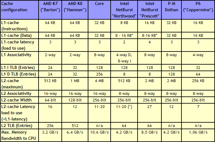 |
| Click to enlarge |
Just a quick look at the numbers in the above table make it clear that the memory subsystem of the Core architecture is impressive. It has twice as much L2 cache as current dual-core CPUs (the same amount as Presler), but the cache is still accessible with low latency. The shared L2 cache also allows one core to use more than 2MB of cache if necessary. Both L1 and L2 cache are accessed via a 256-bit wide bus, allowing the caches to deliver massive bandwidth to the core.
Core versus Hammer: Memory subsystem
Core's most important competitor, the Hammer ("K8") architecture, has two small but noteworthy advantages. The first is its bigger 2 x 64 KB L1 cache. This is only a small advantage as an 8-way 32 KB cache will have a hit rate close to that of a 2-way 64 KB cache.The second and more important advantage is the on die memory controller, which lowers the latency to the memory considerably. However, the lower clockspeeds of the Core CPUs (relative to NetBurst) and the faster FSB also lower latency significantly. With the numbers available to us now, we have reason to believe that the Athlon 64 X2's latency advantage will shrink to only 15 to 20%. For comparison, the memory subsystem of the Pentium 4 was almost twice as slow as the Athlon 64 (80-90 ns versus 45-50 ns).
However, those two small advantages are likely negated by all the other memory subsystem metrics. The Core CPUs have much bigger caches and much smarter prefetching than the competition. The Core architecture's L1 cache delivers about twice as much bandwidth (Measured by ScienceMark), while it's L2-cache is about 2.5 times faster than the Athlon 64/Opteron one.
Smarter Decoding
Similar to the K8 architecture, Core pre-decodes instructions that are fetched. Pre-decode information includes instruction length and decode boundaries.A first for the x86 world, the Core architecture is equipped with four x86 decoders, 3 simple decoders and 1 complex decoder. The task of the decoders - for all current x86 CPUs - is not only to decipher the incoming instruction (opcode, addresses), but also to translate the 1 to 15 byte variable length x86 instructions into - easier to schedule and execute - fixed length RISC-like instructions (called micro-ops).
The most common x86 instructions are translated into a single micro-op by the 3 simple decoders. The complex decoder is responsible for the instructions that produce up to 4 micro-ops. The really long and complex x86 instructions are handled by a microcode sequencer. This way of handling the complex most CISC-y instructions has been adopted by all modern x86 CPU designs, including the P6, Athlon (XP and 64), and Pentium 4.
There is still more to the Core decoders. The first clever technique is macro-op fusion. It makes it possible for two relatively common x86 instructions to be fused into a single instruction. For example, the x86 compare instruction (CMP) is fused with a jump (JNE TARG). These instructions are typically the assembler result of a compiled if-then-else statement.
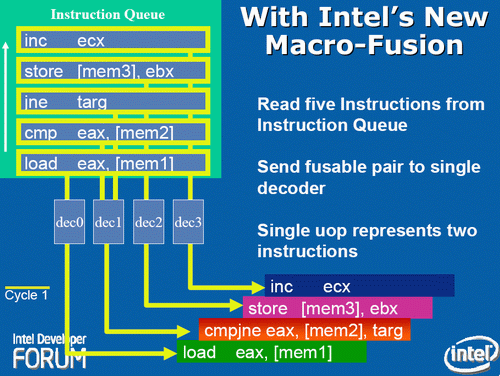
The result is that on average in a typical x86 program, for every 10 instruction, two x86 instructions (called macro-ops by Intel) are fused together. When two x86 instructions are fused together, the 4 decoders can decode 5 instructions in one cycle. The fused instruction travels down the pipeline as a single entity, and this has other advantages: more decode bandwidth, less space taken in the Out of Order (OoO) buffers, and less scheduling overhead. If Intel's "1 out of 10" claims are accurate, macro-ops fusion alone should account for an 11% performance boost relative to architectures that lack the technology.
The second clever technique already exists in the current P-M CPUs. There are a few x86 instructions which are pretty complex to perform, but which are at the same time a very typical and common x86 instruction. We are talking for example about mathematical operations where an address is referenced instead of a register. One common example is ADD [mem], EAX . This means add the content of register EAX to the content of a certain memory location (i.e. store the result back at the memory address). Store instructions which get broken down into store address and store data are another example.
In earlier designs such as the P6 (Pentium Pro, PII, PIII) architecture, these instruction would have been broken up into two or even three micro-ops. Remember that the whole philosophy behind all modern x86 CPUs, since the P6, is to decode x86 instructions into RISC-y micro-ops which are then fed to a fast RISC backend; the backend then schedules, issues, executes and retires the instructions in a smooth RISC way.
There is no way you could feed such an instruction (ADD [mem], EAX) to RISC execution units. It violates every RISC rule. RISC designs all load their data into the registers and then perform the necessary calculation on the registers.
So ADD [mem], EAX is broken down into:
Load the contents of [mem] into a register (Since Banias, the ALU and the Load operation are kept together in one micro-op. This is called micro-op fusion. This is no small feat: in older designs keeping the load and ALU operation together would result in pipeline stages that take much longer and thus lower the maximum clock frequency. (In CPU designs, the maximum clock speed is essentially determined by the slowest possible pipeline stage execution time.) Only by using bigger, smarter circuitry that can do a lot in parallel is micro-op fusion possible without lowering the clock speed significantly.MOV EBX, [mem])
An ALU operation, ADD the two registers together (ADD EBX, EAX)
Store the result back to memory (MOV [mem], EBX)
The pre-decode stage recognizes the macro-ops (or x86) instructions that should be kept together. In the decoding phase, ADD [mem], EAX results in one micro-op. Again, this means that the CPU can stuff more instructions in the same OoO buffers, increasing efficiency and improving performance.
Core versus Hammer: Decoding
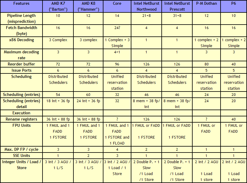
All very nice, but let us take a look at what really matters: How do the 3 simple + 1 complex decoders of Core compare to the 3 complex decoders of AMD's K8 architecture?The original Athlon ("K7") has two way of decoding, Vector and Direct Path. The Vector Path decoding results in more than two RISC-like instructions (called "macro-ops" by AMD), the Direct Path in one, sometimes two macro-ops. Each of the decoders in K7 can handle both Vector Path and Direct Path decoding, but from a performance standpoint Direct Path is preferred since it results in fewer macro-ops. If you're wondering why were discussing K7 all of a sudden, just as Core is largely based off the P6 architecture, K8 is largely based off the K7 architecture.
The 3 complex decoders are powerful and can decode most x86 instructions, with few instructions requiring the Vector Path. The only downside of the K7 decoders is that some FP instructions and SSE instructions have to pass through the Vector Path. K8 has even stronger complex decoders and almost all FP and SSE instructions are also now decoded through the Direct Path decoders. This is possible as fetching and decoding takes more stages than it did in the K7; the K8 architecture is clearly more powerful when it comes to SIMD.
Obviously, Intel's Macro-op ( x86 instruction ) fusion does not exist in AMD's K8. However, micro-op fusion is available in another form. If we compare Intel's and AMD's macro-ops and micro-ops, it is easy to get confused. Take a look at the table below which explains the differences.
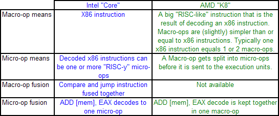
Micro-op fusion does exist in the Athlon. An ADD [mem], EAX is kept together in one macro-op as it travels through the pipeline. Therefore it will take only one place in the OoO buffers. However, the load and execute SSE/SSE2 operations can be fused on Core, while this is not the case on K8: packed SSE operations result in two macro-ops.
So how do Intel's Core and AMD's Hammer compare when it comes to decoding? It is hard to say at the moment without access to Intel's optimization manuals. However, we can get a pretty good idea. In almost every situation, the Core architecture has the advantage. It can decode 4 x86 instructions per cycle, and sometimes 5 thanks to x86 fusion. AMD's Hammer can do only 3.
The situation where AMD's 3 complex decoders can outperform Core's 1 complex + 3 simple decoders is much less likely to happen. It would happen when 3 instructions would be fetched that would have to be handled by the complex decoder of the Core CPU, but which are not too complex that the Microcode Sequencer must kick in. Since the most used x86 instructions all map to one Intel micro-op, this is pretty unlikely.
Out of Order execution: AMD versus Intel
To make this article more accessible and to make the differences between the AMD K8 and the new Intel Core architecture more clear, I tried to make both CPU diagrams in the same style. Here's the Core architecture overview: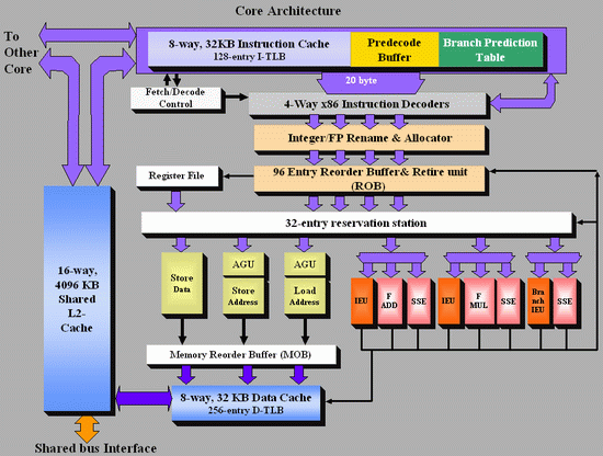
And here's the K8 architecture:
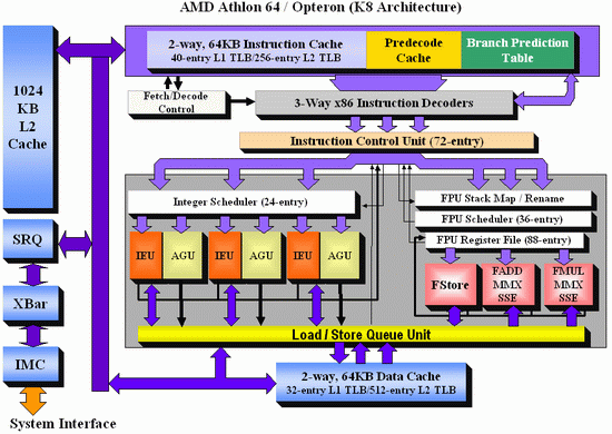
There are a few obvious differences: Core has bigger OoO buffers: the 96 entry ROB buffer is - also thanks to Macro-op fusion - quite a bit bigger than the 72 Entry Macro-op buffer of K8. The P6 architecture could order only 40 instructions, this was doubled to 80 in the P-M architecture (Banias, Dothan, Yonah), and now it's increased even further to 96 for the Core architecture. We've created a table which compares the most important architectural details of several current CPU families:
 |
| Click to enlarge |
The Core architecture uses a central reservation station, while the Athlon uses distributed schedulers. The advantage of a central reservation station is that utilization is better, however distributed schedulers allow more entries. NetBurst also uses distributed schedulers.
Using a central reservation station is another clear example of how Core is in fact the "P8", the second big improvement of the P6 architecture. Just like the P6 architecture, it uses a Reservation Station (RS) and allocates a specific execution unit to execute the micro-op. After execution, the micro-op results are stored in the ROB entry for that micro-op. This aspect of the Core design is clearly taken from the Yonah, Dothan and P6 architectures.
The biggest differences are not immediately visible on the diagrams above. Previous Intel architectures can only perform one branch prediction every two cycles, but Core can sustain one branch per cycle. The Athlon 64 can also perform one branch prediction per cycle.
Another impressive area is Core's SSE multimedia power. Three very powerful 128-bit SSE/SSE2/SSE3 units are available, and two of them are symmetric. Core will outperform the Athlon 64 vastly when it comes to 128-bit SSE2/3 processing.
On K8, 128-bit SSE instructions are decoded into two separate 64-bit instructions. Each Athlon 64 SSE unit can only do one 64-bit instruction at a time, so the Core architecture has essentially at least 2 times the processing power here. With 64-bit FP, Core can do 4 Double Precision FP calculations per cycle, while the Athlon 64 can do 3.
When it comes to integer execution resources, the Core architecture is an improvement over the Pentium 4 and Dothan CPUs, and is at the same level (if we only look at the number of execution units) as the Athlon 64. The Athlon 64 seems to have a small advantage when it comes to calculating addresses: it has 3 AGU compared to Core's 2. This could give the Athlon 64 an advantage in some less common integer workloads such as decrypting algorithms. The deeper, more flexible (Memory disambiguation, see further) out of order buffers and bigger, faster L2-cache of the Core should negate this small advantage in most integer workloads.
Out of Order Loads done right
Since the Pentium Pro, x86 CPUs have been capable of issuing and executing instructions out of order. However, on average one third of the instructions in those reorder buffers could not be reordered easily: we are talking about loads. Moving loads forward can give a very big boost to performance. Instead of loading a piece of data when you need it, it is much more useful to start the load as early as you can. That way, L1 and even L2-cache latencies can be much more easily hidden.This is pretty easy to understand. Imagine having an ALU operation that needs a certain piece of data but that the data is not available in the L1-cache. If the load has been executed many cycles before the ALU operation needs that piece of data, the L2-cache latency is going to have a reduced impact. Of course, you don't want to load a value which is being or will be written to by a previous - following the program/thread order - store. That would mean you are loading an old value, not the up to date one. Check out the picture below.
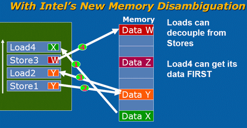
Load 2 cannot be moved forward, since it has to wait until the first Store is done. Only after Store 1 is done will variable Y have its correct value. However there is no reason why Load 4 cannot move forward. It doesn't have to wait for Store 3 and store 1 to finish. By moving Load 4 forward, you give the load unit more time to get the right operand, as we assume that after load 4 a calculation with operand Y will happen.
Currently, CPUs will generally delay load 4 when a store is in flight (active). The problem is the address to which the stores will write has yet to be calculated. To be more precise, the memory addresses are still unknown during reordering and scheduling. When a Load micro-op enters the ROB, the memory addresses of previous stores (from the program order) are not known until they pass the AGU (Address Generation Units).
However, the risk that a load will load a value out of an address that is being written to by a store that has yet to be finished is pretty small (1-2%). That is why Jack Doweck of the Core development team decided to allow Loads to go ahead of previous stores, assuming that the load will not be loading information that will be updated by that preceding store. To avoid that the assumption was wrong, a predictor is used to help. The dynamic alias predictor tries to predict whether or not a previous store will write to the same address as the address from which the load - that you want to execute earlier, thus out of order - will load its data.
Based on Jack Doweck's comments and a study of Intel's previous P6 and P-M architectures I drew up the scheme below. Be warned that this is not the official Intel diagram.
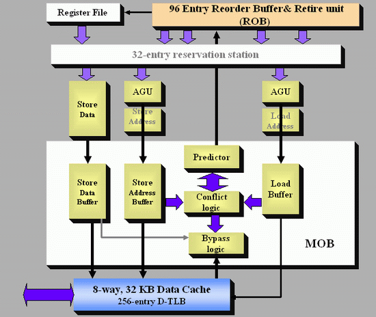
The predictor gives the ReOrder Buffer (ROB) the permission to move a load ahead of a store or not. After the Load has been moved ahead and executed, the conflict logic scans the store buffer located in the Memory reOrder Buffer (MOB) to see if any of the stores which were located before the load (following program order) have written to the address of the out of order load. If so, the load must be redone, and the misprediction penalty is about 20 lost cycles. (Note that the branch misprediction penalty is also about 20 cycles). Worst case, the new dynamic alias predictor may slightly reduce performance, but realistically it's four steps forward, one step back, resulting in a net performance boost.
Determining whether a load and a store share the same address is called memory disambiguation. Allowing loads to move ahead of stores gives a big performance boost. In some snippets of benchmarking code, Intel saw up to a 40% performance boost, solely the result of the more flexible way Loads get reordered. It is pretty clear that we won't see this in most real applications, but it is nevertheless impressive and it should show tangible (10-20%) performance boosts together with the fast L2 and L1 cache.
Let us not forget that loads are probably the most important instructions of all. Not only are loads about one third of the micro-ops that are in flight in a x86 CPU, but they can also cause costly stalls when a load needs to go to the L2 cache (or worse, system memory). So how does this super flexible reordering of loads compare with other architectures?
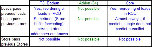
The P6 and P-M could already reorder Loads pretty good. They could move one Load before other Loads, as well as before Stores which have no unknown addresses or addresses which do not reference the same address as the load. In contrast, the Athlon 64 can only move loads before independent ALU operations (ADD etc.). Loads cannot be moved ahead much at all to minimize the effect of a cache miss, and other loads cannot be used to keep the CPU busy if a load has to wait for a store to finish. This means that the Athlon 64 processor is severely limited when it comes to reorder code.
This is probably one of the most important reasons why the Athlon 64 does not outperform the P-M in gaming and integer workloads despite having a lower latency memory system and more integer execution sources. Integer workloads tend to jump around in memory, and have many unknown addresses which must be calculated first. It is less important for FP intensive loads, which is also one of the reasons why the Athlon 64 had no problem with Dothan in this kind of workload. FP workloads access the memory in a much more regular fashion.
Once Loads and Stores are in the queues of Load/Store units, the Athlon's L/S unit allows Loads to bypass Stores, except of course when the load would bypass a store to the same address. Unfortunately, by then the Loads are already out of the ICU and cannot be used to fill the holes that dependencies and cache misses make. You could say that the Athlon (64) has some Load/Store reordering but it's much later in the pipeline and is less flexible than the P6, P-M, and Core architectures.
What about Hyper-Threading and IMC?
Core's impressive execution resources and massive shared cache seem to make it the ideal CPU design for SMT. However, there is no Simultaneous Multi Threading anywhere in the Core architecture. The reason is not that SMT can't give good results (See our elaborate discussion here), but that the engineers were given the task to develop a CPU with a great performance ratio that could be used for the Server, Desktop and Mobile markets. So the designers in Israel decided against using SMT (Hyper-Threading). While SMT can offer up to a 40% performance boost, these performance benefits will only be seen in server applications. SMT also makes the hotspots even hotter, so SMT didn't fit very well in Core's "One Micro-Architecture to Rule them All" design philosophy.As far as including an Integrated Memory Controller (IMC), we were also told that the transistors which could have been spent in the IMC were better spent in the 4 MB shared cache. This is of course highly debatable, but it is a fact cache consumes less power. The standard party line from Intel is that keeping the memory controller on the chipset allows them to support additional memory types without having to re-spin the CPU core. That is certainly true, and with the desktop/mobile sectors using standard DDR2 while servers are set to move to FB-DIMM designs, the added flexibility isn't terrible. Techniques such as memory disambiguation and improved prefetch logic can also help to eliminate any advantage an IMC might offer. Would an IMC improve Core's performance? Almost certainly, but Intel will for the time being pursue other options.
Conclusion 1 : AMD K8 versus Intel P8
The Intel Core architecture is clearly the heir and descendant of the hugely successful P6 architecture. However, it has state of the art technology on board such as micro-op/macro-op fusion, memory disambiguation and massive SIMD/FP power.Compared to the excellent AMD K8/Hammer architecture, the Core CPU is simply a wider, more efficient and more out of order CPU. When I suggested to Jack Doweck that the massive execution resources may not be fully used until SMT is applied, he disagreed completely. Memory disambiguation should push the current limits of ILP in integer loads a lot higher, and the massive bandwidth that the L1 and L2 can deliver should help Core to come close to the execution utilization percentages of the current P-M. 33% more execution potential could thus come very close to 33% more performance, clock-for-clock.
So is it game over for AMD? Well, if you read the previous pages, it is pretty clear that there are some obvious improvements that should happen in AMD's next generation. However, there is no reason at all to assume that the current K8 architecture is at the end of its life. One obvious upgrade possibility is to enhance the SSE/SIMD power by increasing the wideness of each unit or by simply implementing more of them in the out of order FP pipeline.
To sustain the extra (SIMD) FP power, AMD should definitely improve the bandwidth of the two caches further. The K7 had a pretty slow L2-cache, and the K8 doubled the amount of bandwidth that the L2 could deliver for example. It's not unreasonable to think a 256-bit wide cache bus could be added to a near-future AMD design.
Finally, there is also a lot of headroom for increasing integer performance. The fact that Loads can hardly be reordered has been a known weak point since the early K7 days. In fact, we know that engineers at AMD were well aware of it then, and it is surprising that AMD didn't really fix this in the K8 architecture. Allowing a much more flexible reordering of Loads - even without memory disambiguation - would give a very healthy boost to IPC (5% and more). It is one of the main reasons why the P-M can beat the Athlon 64 clock-for-clock in certain applications.
Those are just a few examples that are well known. It is very likely that there are numerous other possible improvements that could take the K8 architecture much further.
Looking at the server version of Core ("Woodcrest") and considering that it is very hard to find a lot of ILP in server applications, the only weakness of Core is that there is no multi-threading in each Core. This small disadvantage is a logical result of the design goal of Core, an architecture which is an all-around compromise for the server, desktop and mobile markets. The lack of Hyper-Threading in Xeon Core products might give Sun and IBM a window of opportunity in the heavy thread server application benchmarks, but since Tigerton (65 nm, two Woodcrests in one package, 4 cores) will come quickly, the disadvantage of not being able to extract more TLP might never be seen. Our astute readers will have understood by now that it is pretty hard to find a weakness in the new Core architecture.
Conclusion 2 : The free lunch is back!
It is ironic that just a year ago, Intel and others were downplaying the importance of increasing IPC and extracting more ILP. Multi-core was the future, single thread performance was a minor consideration. The result was that the reputed Dr. Dobbs journal headlined : "the free lunch is over" [1] claiming that only larger caches would increase IPC a little bit and that the days that developers could count on the ever increasing clockspeeds and IPC efficiency of newer CPU to run code faster were numbered. Some analysts went even further and felt that CPU packages with many relatively simple, small in-order CPUs were the future.At AnandTech, we were pretty skeptical about the "threading is our only savior" future, as Tim Sweeney, the leading developer behind the Unreal 3 engine, explained the challenges of multi-threaded development of the next generation of games. The fat, wide OoO core running at high clockspeeds was buried a little too soon. Yes, Intel's Core does not use the aggressive domino and LVS circuit-design strategy that NetBurst designs used to achieve stunning clockspeeds. At the same time, it is a fat, massive reordering CPU which gives free lunch to developers who don't want to spend too much time on debugging heavily threaded applications. Multi-core is here to stay, but getting better performance is once again the shared responsibility of both the developer and the CPU designer. Yes, dual-core is nice, but single threaded performance is still important!
I would like to express my thanks to the following people who helped to make this article possible:
Jack Doweck, "Foo", "Redpriest", Jarred and Anand
References
[1] The Free Lunch Is Over: A Fundamental Turn Toward Concurrency in Software By Herb SutterIntel's Next Generation Microarchitecture Unveiled, by David Kanter, Real World Technologies


