Original Link: https://www.anandtech.com/show/1865
Inside Microsoft's Xbox 360 - A Tour of the 360's Motherboard
by Anand Lal Shimpi on November 18, 2005 12:19 AM EST- Posted in
- Systems
On Wednesday we took apart the Xbox 360 to satisfy our curiosities and provide a tutorial to all those willing to take time out of gaming in order to take theirs apart as well. Today, we take a bit of a different approach, focusing on one item within the sleekly design chassis in particular - the Xbox 360 motherboard.
We've been reviewing motherboards on AnandTech for over eight years now, so of course taking look at the Xbox 360's motherboard in greater detail is right up our alley. Before proceeding, we recommend taking a look at our Inside the Xbox 360 article, which diagrams taking it apart as well as provides a brief overview of the technology in the system.
The original Xbox featured a 4-layer Intel motherboard, but given the incredible power requirements of the CPU and GPU on the Xbox 360's motherboard we would be astonished if the same were true today. Luckily with any console, especially early on in their life, you are getting a true bargain when it comes to the cost of hardware - so the number of layers on this PCB doesn't matter much to the end user, as Microsoft will absorb all costs above and beyond the core system's $299 price tag.
We've already shown a picture of the motherboard, but here's another shot as a refresher:
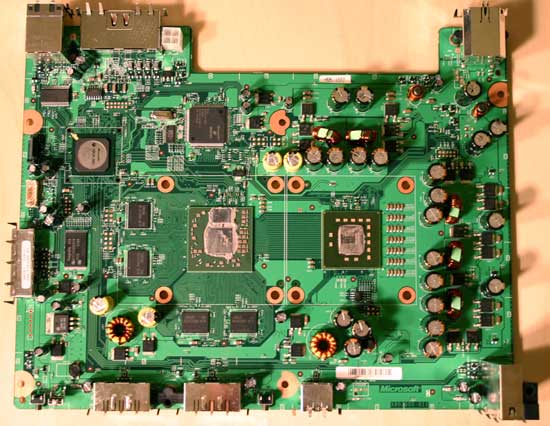
To help you orient yourself, the bottom of the picture is the front of the unit and the left of the picture is where you would see the optional hard drive. Keep this picture in mind as we go through the tour of the motherboard, as you'll see a thumbnail of this board in almost every picture in the coming pages, with the component we're discussing at the time circled in red.
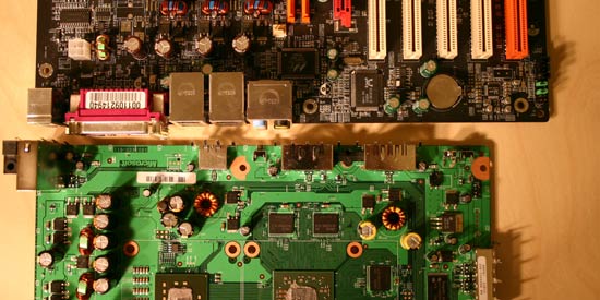
The motherboard is quite small in order to give the Xbox 360 a much more slender look compared to its predecessor, which basically used a regular sized ATX motherboard. Below we have a picture of it lined up next to a standard ATX motherboard - in this case a MSI K8N Neo2:
With the size put in perspective, let's begin the tour.
The Motherboard's Ports
Of course with a custom design like the Xbox 360's motherboard, you end up with the perfect layout, as it is built to fit the chassis. The original Xbox debuted with no legacy ports and with USB ports disguised as controller ports, the 360 continues in the tradition with an update to USB 2.0.
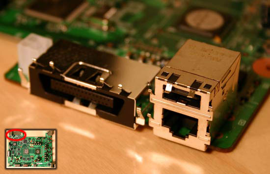
At the rear of the console you've got the AV cable port (left), a single USB port and an Ethernet jack:
Unfortunately in the first version of the Xbox 360, that AV cable port appears to be strictly analog. Microsoft has indicated that they may support HDMI at a later point in time, but that may require a new revision of the motherboard - assuming there is no digital video signal carried over the AV port. On the flip side, ATI has had a history of placing TMDS transmitters on their GPUs, so it may be possible that a digital video signal is present at this connector today, although if it were we don't understand why Microsoft wouldn't offer a DVI/HDMI cable option now.
To the left of the AV cable port there's a 4-pin power connector similar to the ATX12V connectors we're used to seeing on motherboards:
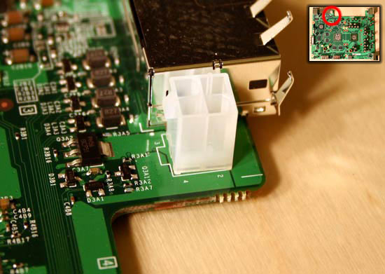
Also at the back you have a very large power connector, to show you the size of it, we've placed a mobile Pentium M processor next to the connector:
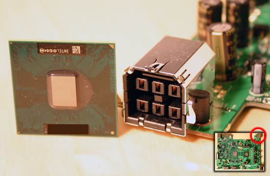
It's big
On the left side of the motherboard we've got the SATA data connector, which is a standard SATA connector for the DVD-ROM drive. Next to it you'll see the custom power connector:
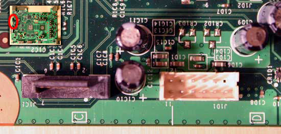
Just slightly to the right of it there's a custom connector which is essentially nothing more than a SATA interface for the optional removable hard drive:
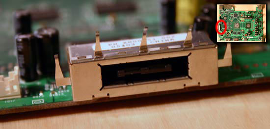
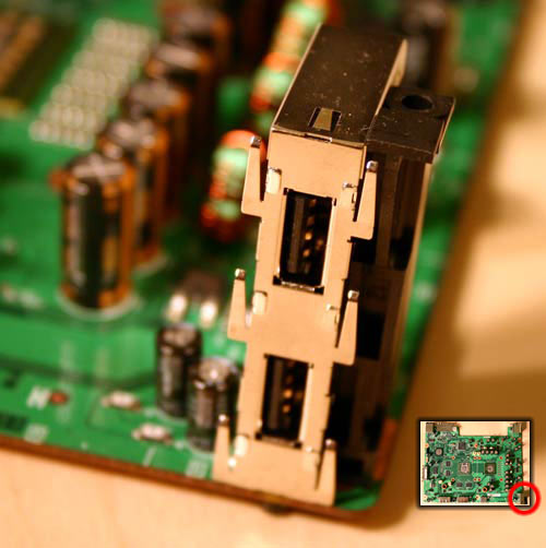
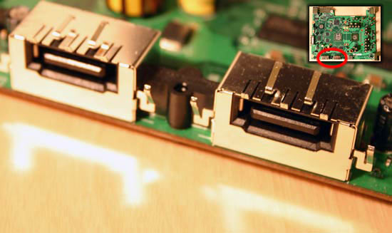
Of course at the front of the board there's a riser with two USB 2.0 ports on it:
The memory cards also have their own interface on the board:
Taking the Surface Tour
Moving away from the ports and looking inwards, we take a look at some of the ICs and other devices present on the Xbox 360's motherboard.
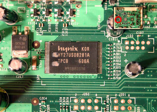
The Xbox 360's OS and other necessary software is loaded in the 128Mb (16MB) NAND Flash device that's on the motherboard:
Originally we assumed the chip below was a TV encoder, but we've since found out that the TV encoder on ATI's Xenos GPU is identical to what is on the ATI Radeon X1000 series of PC graphics cards - meaning the Xbox 360's TV encoder is located on the Xenos GPU itself and makes use of ATI's Xilleon display engine.
If it isn't the TV encoder, then what is this mystery chip? We haven't been able to find the physical interface for the Ethernet port, so it is possible that the 100Mbit PHY is located within this chip, as well as the audio codec, both of which would make sense given its location on the motherboard (within close proximity to the AV cable connector). In addition to those two options, it is possible that this chip may house whatever DRM technology is used in the Xbox 360.
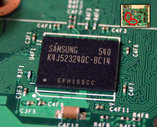
Next up we've got a single 64MB Samsung GDDR3 memory device from the Xbox 360's motherboard; there are a total of 8 of these chips on the motherboard, adding up to the system's full 512MB of unified system memory. The part number on the chip indicates a 700MHz operating frequency, with a 1.4Gbps/pin data rate, which is exactly what is specified by Microsoft:
Up Close and Personal with the CPU, GPU and... Yonah?
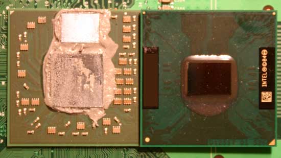
The heart and soul of the Xbox 360 is of course its CPU and GPU, first off we have the 3 core PowerPC processor. In order to give you an idea of its size, we've compared it here to Intel's 65nm Yonah processor, with a die size of just 90 mm^2:
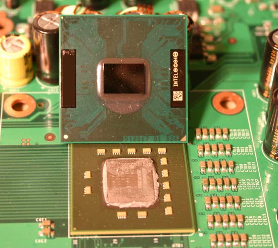
The 90nm Xenon processor looks to be a little less than 3 Yonahs, but remember that the move to 65nm will cut the Xenon basically in half, making it closer to 1.5 Yonahs if they were on the same manufacturing process. Through this comparison we can get a rough idea of the size of the logic in the Xenon CPU.
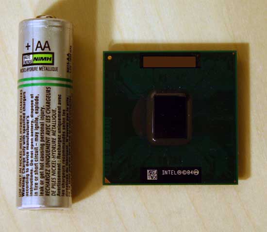
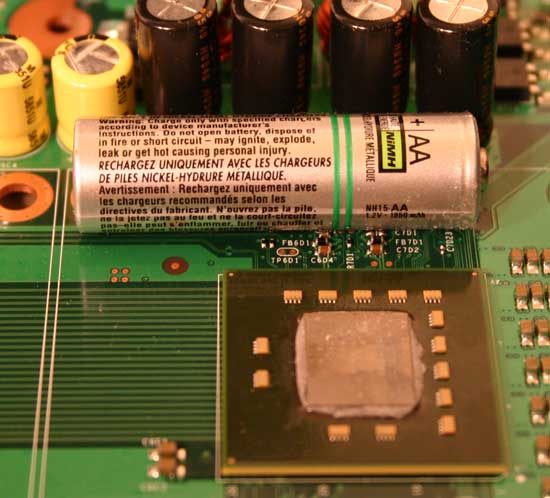
As another comparison point, here is Yonah vs. a AA battery, as well as the 3-core Xenon processor with a AA battery:
Now let's have a look at Yonah vs. the ATI Xenos GPU:
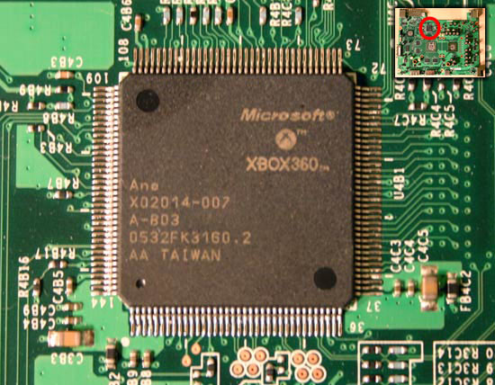
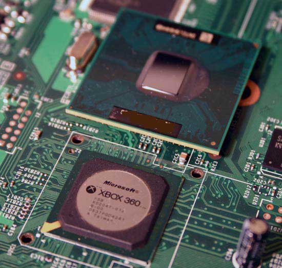
Finally we've got the Xbox 360 South Bridge, which is quite small:
Final Words, and a Refresher on the Benefits of Serial Buses
We hope you enjoyed this brief tour of the Xbox 360's motherboard, being the last weekend before Microsoft's official retail launch, we figured it would be a good send-off.
We'll actually end this tour of the 360's motherboard with a little comparison point in the advancement of bus technologies. For the past several years, the PC industry has seen a transition away from older parallel bus interfaces (IDE, Parallel Ports, traditional FSBs, PCI/AGP) to much faster serial buses (SATA, USB, Hyper Transport, PCI Express). The Xbox 360's motherboard actually gives us an opportunity to present a good comparison of the benefits of a serial interface, from a layout perspective.
The link between the Xenon CPU and the Xenos GPU in the Xbox 360 is actually two 10.8GB/s serial buses, which you can clearly see from the picture below. Note the clear definition of the traces the clean routing, to the point where you can count the individual data, address and clock lines:
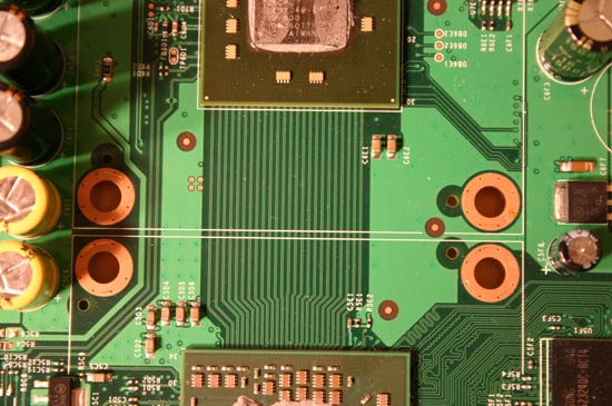
This is similar to the type of routing you'd see connecting two Hyper Transport ports on an AMD motherboard.
Now let's take a look at the parallel GDDR3 interface between the ATI GPU and the Samsung GDDR3 memory:
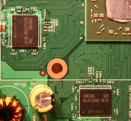
Note the significant increase in traces, attributed to a much wider parallel interface than what exists between the CPU and GPU. The more complex routing of parallel buses becomes an even bigger problem as devices demand more bandwidth, which is why we have seen such a large scale transition to serial interfaces.


