Original Link: https://www.anandtech.com/show/1689
E3 2005 - Day 2: More Details Emerge on Console GPUs
by Anand Lal Shimpi on May 19, 2005 1:24 PM EST- Posted in
- Trade Shows
This year's E3 has been, overall, a pretty big letdown. The show itself hasn't been very interesting simply because it's mostly current-gen titles and hardware. For the E3 just before the launch of Microsoft's Xbox 360, we were a bit disappointed not to see any working hardware at the show outside of the ATI booth.
With a relatively light schedule thanks to the small size of the show, we were able to spend quite a bit of time digging deeper on the two highlights of this year's E3 - ATI's Xbox 360 GPU, and NVIDIA's RSX, the GPU powering the PlayStation 3.
Given that both of the aforementioned GPU designs are very closely tied to their console manufacturers, information flow control was dictated by the console makers, not the GPU makers. And unfortunately, neither Microsoft or Sony were interested in giving away more information than their ridiculously light press releases.
Never being satisfied with the norm, we've done some digging and this article is what we've managed to put together. Before we get started, we should mention a few things:
1) Despite our best efforts, information will still be light because of the strict NDAs imposed by Microsoft and Sony on the GPU makers.
2) Information on NVIDIA's RSX will be even lighter because it is the more PC-like of the two solutions and as such, a lot of its technology overlaps with the upcoming G70 GPU, an item we currently can't talk about in great detail.
With those items out of the way, let's get started, first with what has already been announced.
The Xbox 360 GPU, manufactured by ATI, is the least PC-like of the two GPUs for a number of reasons, the most obvious being its 10MB of embedded DRAM. Microsoft announced that the 10MB of embedded DRAM has 256GB/s of bandwidth availble to it; keep this figure in mind, as its meaning isn't as clear cut as it may sound.
The GPU operates at 500MHz and has a 256-bit memory interface to 512MB of 700MHz GDDR3 system memory (that is also shared with the CPU).
Another very prominent feature of the GPU is that it implements ATI's first Unified Shader Architecture, meaning that there are no longer any discrete pixel and vertex shader units, they are instead combined into a set of universal execution units that can operate on either pixel shader or vertex shader instructions. ATI is characterizing the width of the Xbox 360 GPU as being 48 shader pipelines; we should caution you that these 48 pipelines aren't directly comparable to current 16-pipeline GPUs, but rest assured that the 360 GPU should be able to shade and texture more pixels per clock than ATI's fastest present-day GPU.
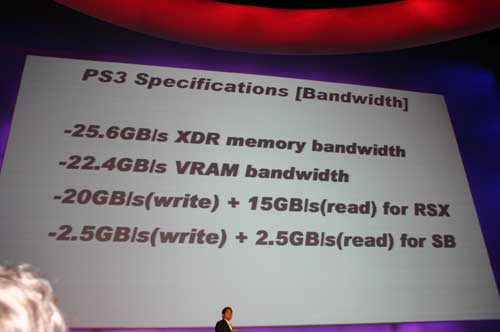
Now let's move on to NVIDIA's RSX; the RSX is very similar to a PC GPU in that it features a 256-bit connection to 256MB of local GDDR3 memory (operating at 700MHz). Much like NVIDIA's Turbo Cache products, the RSX can also render to any location in system memory, giving it access to the full 256MB of system memory on the PS3 as well.
The RSX is connected to the PlayStation 3's Cell CPU by a 35GB/s FlexIO interface and it also supports FP32 throughout the pipeline.
The RSX will be built on a 90nm process and features over 300 million transistors running at 550MHz.
Between the two GPUs there's barely any information contained within Microsoft's and Sony's press launches, so let's see if we can fill in some blanks.
More Detail on the Xbox 360 GPU
ATI has been working on the Xbox 360 GPU for approximately two years, and it has been developed independently of any PC GPU. So despite what you may have heard elsewhere, the Xbox 360 GPU is not based on ATI's R5xx architecture.
Unlike any of their current-gen desktop GPUs, the 360 GPU supports FP32 from start to finish (as opposed to the current FP24 spec that ATI has implemented). Full FP32 support puts this aspect of the 360 GPU on par with NVIDIA's RSX.
ATI was very light on details of their pipeline implementation on the 360's GPU, but we were able to get some more clarification on some items. Each of the 48 shader pipelines is able to process two shader operations per cycle (one scalar and one vector), offering a total of 96 shader ops per cycle across the entire array. Remember that because the GPU implements a Unified Shader Architecture, each of these pipelines features execution units that can operate on either pixel or vertex shader instructions.
Both consoles are built on a 90nm process, and thus ATI's GPU is also built on a 90nm process at TSMC. ATI isn't talking transistor counts just yet, but given that the chip has a full 10MB of DRAM on it, we'd expect the chip to be fairly large.
One thing that ATI did shed some light on is that the Xbox 360 GPU is actually a multi-die design, referring to it as a parent-daughter die relationship. Because the GPU's die is so big, ATI had to split it into two separate die on the same package - connected by a "very wide" bus operating at 2GHz.
The daughter die is where the 10MB of embedded DRAM resides, but there is also a great deal of logic on the daughter die alongside the memory. The daughter die features 192 floating point units that are responsible for a lot of the work in sampling for AA among other things.
Remember the 256GB/s bandwidth figure from earlier? It turns out that that's not how much bandwidth is between the parent and daughter die, but rather the bandwidth available to this array of 192 floating point units on the daughter die itself. Clever use of words, no?
Because of the extremely large amount of bandwidth available both between the parent and daughter die as well as between the embedded DRAM and its FPUs, multi-sample AA is essentially free at 720p and 1080p in the Xbox 360. If you're wondering why Microsoft is insisting that all games will have AA enabled, this is why.
ATI did clarify that although Microsoft isn't targetting 1080p (1920 x 1080) as a resolution for games, their GPU would be able to handle the resolution with 4X AA enabled at no performance penalty.
ATI has also implemented a number of intelligent algorithms on the daughter die to handle situations where you need more memory than the 10MB of DRAM on-die. The daughter die has the ability to split the frame into two sections if the frame itself can't fit into the embedded memory. A z-pass is done to determine the location of all of the pixels of the screen and the daughter die then fetches only what is going to be a part of the scene that is being drawn at that particular time.
On the physical side, unlike ATI's Flipper GPU in the Gamecube, the 360 GPU does not use 1T-SRAM for its on-die memory. The memory on-die is actually DRAM. By using regular DRAM on-die, latencies are higher than SRAM or 1T-SRAM but costs should be kept to a minimum thanks to a smaller die than either of the aforementioned technologies.
Remember that in addition to functioning as a GPU, ATI's chip must also function as a memory controller for the 3-core PPC CPU in the Xbox 360. The memory controller services both the GPU and the CPU's needs, and as we mentioned before the controller is 256-bits wide and interfaces to 512MB of unified GDDR3 memory running at 700MHz. The memory controller resides on the parent die.
Scratching the Surface of NVIDIA's RSX
As we mentioned before, NVIDIA's RSX is the more PC-like of the two GPU solutions. Unlike ATI's offering, the RSX is based on a NVIDIA GPU, the upcoming G70 (the successor to the GeForce 6).
The RSX is a 90nm GPU weighing in at over 300 million transistors and fabbed by Sony at two plants, their Nagasaki plant and their joint fab with Toshiba.
The RSX follows a more conventional dataflow, with discrete pixel and vertex shader units. Sony has yet to announce the exact number of pixel and vertex shader units, potentially because that number may change as time goes by depending on yields. This time around Sony seems to be very careful not to let too many specs out that are subject to change to avoid any sort of backlash as they did back with the PS2. Given the transistor count and 90nm process, you can definitely expect the RSX to feature more than the 16 pipes of the present day GeForce 6800 Ultra. As for how many, we'll have to wait for Sony on that.
NVIDIA confirmed that the RSX is features full FP32 support, like the current generation GeForce 6 as well as ATI's Xbox 360 GPU. NVIDIA did announce that the RSX would be able to execute 136 shader operations per cycle, a number that is greater than ATI's announced 96 shader ops per cycle. Given that we don't know anything more about where NVIDIA derived this value from, we can't be certain if we are able to make a direct comparison to ATI's 96 shader ops per cycle.
Given that the RSX is based off of NVIDIA's G70 architecture, you can expect to have a similar feature set later this year on the PC. In fact, NVIDIA stated that by the time PS3 ships there will be a more powerful GPU available on the desktop. This is in stark contrast to ATI's stance that a number of the features of the Xbox 360 GPU won't make it to the desktop for a matter of years (potentially unified shader architecture), while others will never be seen on the desktop (embedded DRAM?).
There will definitely be some differences between the RSX GPU and future PC GPUs, for a couple of reasons:
1) NVIDIA stated that they had never had as powerful a CPU as Cell, and thus the RSX GPU has to be able to swallow a much larger command stream than any of the PC GPUs as current generation CPUs are pretty bad at keeping the GPU fed.
2) The RSX GPU has a 35GB/s link to the CPU, much greater than any desktop GPU, and thus the turbo cache architecture needs to be reworked quite a bit for the console GPU to take better advantage of the plethora of bandwidth. Functional unit latencies must be adjusted, buffer sizes have to be changed, etc...
We did ask NVIDIA about technology like unified shader model or embedded DRAM. Their stance continues to be that at every GPU generation they design and test features like unified shader model, embedded DRAM, RDRAM, tiling rendering architectures, etc... and evaluate their usefulness. They have apparently done a unified shader model design and the performance just didn't make sense for their architecture.
NVIDIA isn't saying that a unified shader architecture doesn't make sense, but at this point in time, for NVIDIA GPUs, it isn't the best call. From NVIDIA's standpoint, a unified shader architecture offers higher peak performance (e.g. all pixel instructions, or all vertex instructions) but getting good performance in more balanced scenarios is more difficult. The other issue is that the instruction mix for pixel and vertex shaders are very different, so the optimal functional units required for each are going to be different. The final issue is that a unified shader architecture, from NVIDIA's standpoint, requires a much more complex design, which will in turn increase die area.
NVIDIA stated that they will eventually do a unified shader GPU, but before then there are a number of other GPU enhancements that they are looking to implement. Potentially things like a programmable ROP, programmable rasterization, programmable texturing, etc...
Final Words
We're going to keep digging on both of these GPUs, as soon as we have more information we'll be reporting it but for now it's looking like this is the best we'll get out of Microsoft and Sony.


