Original Link: https://www.anandtech.com/show/1491
RAM - Memory Technology Overview
by Jarred Walton on September 28, 2004 12:05 AM EST- Posted in
- Memory
Introduction
If you have ever asked for advice on what type of RAM to purchase, you were probably given a response that goes something as follows. The higher the supported bandwidth of the RAM, the better, but having lower timings is also important. Both options of course bring along price increases, and buying cheaper "generic" RAM is seldom recommended. The old adage of "you get what you pay for" is often used. This is all sound advice, but what does it really mean? Why is CL2 RAM better than CL2.5 or CL3? What about the other features, like bandwidth? Higher bandwidth is often mutually exclusive to having the best timings, so which is better?We have planned a series of articles to cover this topic, and in this first part, we will provide a general overview of memory technology and terms, and how they actually affect performance. Specific examples using one type of RAM may be included, but we are saving a detailed comparison of the DRAM types for the next article in this series. For this introduction, we are interested in growing the base of knowledge upon which future articles can be built.
Before we get into the details of memory designs, we would like to simply state up front that anyone who thinks that DRAM technology, design, and implementation are "easy" or "boring" relative to the higher profile CPU and GPU chips is guilty of a gross generalization. While it might be true that an individual DRAM chip is less complex, the memory subsystem as a whole can easily rival other parts for complexity. It should come as little surprise that in a modern PC, system RAM can often cost more on its own than any other component, with the exception of bleeding edge processors and graphics cards. The design problems and solutions can be every bit as interesting - or difficult, if you prefer - as pipelines, execution units, and cache sizes.
Memory Access Overview
In order to understand the meaning of the various timings on RAM, we need to first look at how memory is accessed. This is still only part of the overall memory subsystem, but it is the portion that relates directly to the memory timings. We will cover the remaining portions of memory access in a moment. Ignoring how a memory request actually gets to the RAM modules, then, the pattern for a memory access is as follows.First, the requested address arrives at the memory module. In a worst case scenario, the address is not contained in one of the currently active rows of memory (also called memory pages), so an active row is flushed out, the new row is requested, the row becomes active, and after a slight delay, the specific column in the row can be requested. There is another delay while the column is accessed, and then the data begins coming across the memory bus. The whole column is not sent across the bus immediately, but is sent in several bursts instead. The number of bursts used in transmitting the data is referred to as the burst length, and these bursts occur at the effective data rate - i.e. two bits per clock on DDR/DDR2 and one bit per clock for SDRAM.
That is a worst case scenario, but luckily, that is not the most common occurrence. Due to spatial locality - which says that if you access one piece of data at address X, you will likely also access the data at X+1, X-1, X+2, X-2, etc. - memory has what is called active rows/pages. These are rows that are stored currently in what amounts to a small cache on the memory chips - this is called a "sense amplifier" - and when a request arrives for data that is already stored in an active row, only the request for a specific column is needed. Row sizes are typically 1KB or 2KB on current DRAMs and column sizes vary according to several other factors such as device width and burst length.
A further explanation of the actual layout of memory is also important. We have talked about rows and columns being accessed, but there is still more to the overall structure. As we had mentioned, rows are also called memory pages, but pages are further grouped into memory banks. Banks of memory can be thought of as something like the set associativity of a cache - each bank can only have one active row at a time. If a second page within a memory bank is requested, the open page must be closed before the new page can be opened. In certain situations, if two different pages within the same bank are requested in rapid succession, additional delays can occur, as a page must remain active for a minimum amount of time. Increasing the number of banks reduces the chance of this happening, so generally speaking, having more banks can help to improve memory performance. There is also a trade off, however, as increasing the number of banks requires additional logic in the memory controller and other components related to the memory subsystem.
Keep this initial explanation of the RAM access pattern in mind when we talk about timings in a moment, but now we need to go back a step and refine our description of how memory is accessed.
Memory Subsystem Overview
We mentioned how changes to the module design can require changes to the memory controller as well. When an address arrives at the memory, it does not simply appear there directly from the CPU; we are really talking about several steps. First, the CPU sends the request to the cache, and if the data is not in the cache, the request is forwarded to the memory controller via the Front Side Bus (FSB). (In some newer systems like the Athlon 64, requests may arrive via a HyperTransport bus, but the net result is basically the same.) The memory controller then sends the request to the memory modules over the memory bus. Once the data is retrieved internally on the memory module, it gets sent from the RAM via the memory bus back to the memory controller. The memory controller then sends it onto the FSB, and eventually, the requested data arrives at the CPU.Note that the data could also be requested/sent somewhere else. DMA (Direct Memory Access) allows other devices such as network adapters, sound cards, graphics cards, controller cards, etc. to send requests directly to the memory controller, bypassing the CPU. In this overview, we were talking about the CPU to RAM pathway, but the CPU could be replaced by other devices. Normally, the CPU generates the majority of the memory traffic, and that is what we will mostly cover. However, there are other uses of the RAM that can come into play, and we will address those when applicable.
Now that we have explained how the requests actually arrive, we need to cover a few details about how the data is transmitted from the memory module(s). When the requested column is ready to transmit back to the memory controller, we said before that it is sent in "bursts". What this means is that data will be sent on every memory bus clock edge - think of it as a "slot" - for the RAM's burst length. If the memory bus is running at a different speed than the FSB, though - especially if it's running slower - there can be some additional delays. The significance of these delays varies by implementation, but at best, you will end up with some "bubbles" (empty slots) in the FSB. Consider the following specific example.
On Intel's quad-pumped bus, each non-empty transmission needs to be completely full, so all four slots need to have data. (There are caveats that allow this rule to be "bent", but they incur a loss of performance and so they are avoided whenever possible.) If you have a quad-pumped 200 MHz FSB (the current P4 bus) and the RAM is running on a double-pumped 166 MHz bus, the FSB is capable of transmitting more data than the RAM is supplying. In order to guarantee that all four slots on an FSB clock cycle contain data, the memory controller needs to buffer the data to make sure an "underrun" does not occur - i.e. the memory controller starts sending data and then runs out after the first one or two slots. Each FSB cycle comes at 5 ns intervals, and with a processor running at 3.0 GHz, a delay of 5 ns could mean as many as 15 missed CPU cycles!
There are a couple of options to help speed up the flow of data from the memory controller to the FSB. One is to use dual-channel memory, so the buffer will fill up in half the time. This helps to explain why Intel benefits more from dual-channel RAM than AMD: their FSB and memory controller are really designed for the higher bandwidth. Another option is to simply get faster RAM until it is able to equal the bandwidth of the FSB. Either one generally works well, but having a memory subsystem with less bandwidth than what the FSB can use is not on ideal situation, especially for the Intel design. This is why most people recommend against running your memory and system busses asynchronously. Running RAM that provides a higher bandwidth than what the FSB can use does not really help, other than to reduce latencies in certain situations. If the memory can provide 8.53 GB/s of bandwidth and the FSB can only transmit 6.4 GB/s, the added bandwidth generally goes to waste. For those wondering why benchmarks using DDR2-533 with an 800 FSB P4 do not show much of an advantage for the faster memory, this is the main reason. (Of course, on solutions with integrated graphics, the additional memory bandwidth could be used for graphics work, and in servers, the additional bandwidth can be helpful for I/O.)
If you take that entire description of the memory subsystem, you can also see how AMD was able to benefit by moving the memory controller onto the CPU die. Now, the delays associated with the transmission of data over the FSB are almost entirely removed. The memory controller still has to do work, but with the controller running at CPU clock speeds, it will be much faster than before. The remaining performance deficit that Athlon 64 and Opteron processors suffer when running slower RAM can be attributed to the loss of bandwidth and the increased latencies, which we will discuss more in a moment. There are a few other details that we would like to mention first.
Features and Design Considerations
We now have a pretty good idea of how memory is accessed, but there are a couple of other topics that are important, which we would like to address. In an ideal world, we would want high bandwidths, low latencies, low costs, and we want it all now. Naturally, all of these goals are in opposition to each other. It is possible, for instance, to create memory that offers both high bandwidth and low latencies, but the cost is considered prohibitive. One item that we have not addressed yet that bears mention is the complexity factor. It is a topic that companies can spend a lot of money examining.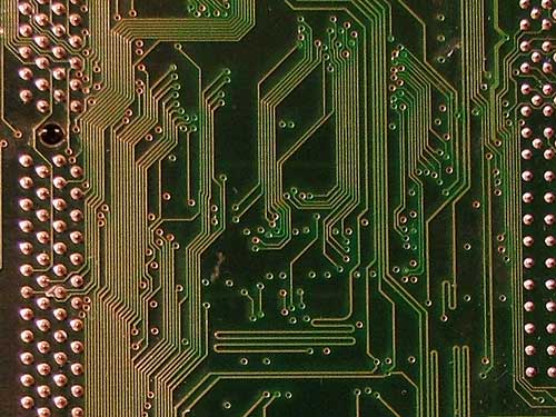
A faster memory interface that is very difficult to work with may end up getting scrapped, or at least delayed. For instance, dual-channel DDR configurations sound better in theory, but the difficulty of routing all of the traces between the RAM slots and the memory controller may not be worth the increased performance. Instead of using four layers in a motherboard or graphics card design, six layers or even eight may be required. Boards with more layers cost more money and more time to produce. Another factor is that in order to make all of the signals on each trace (wire) on the board arrive at the same time, they should be the same length. This requirement can lead to the "serpentining" of traces - a trace that zigzags back and forth in order to make it longer - as you can see in the above image. Testing and validation of motherboards become increasingly difficult as the number of traces and layers increase. Needless to say, determining the optimal configuration for a board design can be a very difficult balancing act.
With increasing clock speeds, signal integrity and interference also become more of a concern. Several trends have been at work lately, and not all of them are desirable. The first is that memory speeds have been increasing. This is desirable, but there are some drawbacks. In order to avoid signaling problems, we have gone from seeing eight RAM modules per memory channel to four modules, and now configurations that only support two modules are common. While DRAM density has been increasing, the reduction in the number of modules has worked against increasing the total memory size. In the server market, where large amounts of RAM are more important than having the fastest memory timings, technologies such as registered memory have helped to combat this. Future plans to help increase RAM size and speed without compromising the signal integrity include the switch to point-to-point connections instead of multi-drop busses, modified signaling algorithms that help to reduce interference, and on-chip signal termination.
As processor speeds increase, it is inevitable that memory performance will also need to improve. Manufacturing technologies have also improved, and so designs that were once too complex may become realizable in the future. Suffice it to say that memory manufacturers are not sitting idle, and there are designs and plans to help meet the increased demands of the future. We will be providing a more detailed look at the various options in the next article. For now, that covers the overview of the basics, and we can now get into some of the deeper details of memory performance.
Memory Timings and Bandwidth Explained
With that brief overview of the memory subsystem, we are ready to talk about memory timings. There are usually four and sometimes five timings listed with memory. They are expressed as a set of numbers, e.g. 2-3-2-7, corresponding to CAS-tRCD-tRP-tRAS. On modules that list a fifth number, it is usually the CMD value, e.g. 1T. Some might also include a range for the tRAS value. These are really only a small subset of the total number of timing figures that memory companies use, but they tend to be the more important ones and encapsulate the other values. So, what does each setting mean? By referring back to the previous sections on how memory is accessed, we can explain where each value comes into play.The most common discussion on timing is the CAS Latency, or CL value. CAS stands for Column Access Strobe. This is the number of memory cycles that elapse between the time a column is requested from an active page and the time that the data is ready to begin bursting across the bus. This is the most common occurrence, and so, CAS Latency generally has the largest impact on overall memory performance for applications that depend on memory latency. Applications that depend on memory bandwidth do not care as much about CAS latency, though. Of course, there are other factors that come into play, as our tests with OCZ 3500EB RAM have shown that a well designed CL2.5 RAM can keep up with and sometimes even outperform CL2 RAM. Note that purely random memory accesses will stress the other timings more than the CL, as there is little spatial locality in that case. Random memory access is not typical for general computing, which explains why theoretical memory benchmarks that use it as a performance metric frequently have little to no correlation with real world performance.
The next value is tRCD, which is referred to as the RAS to CAS Delay. This is the delay in memory cycles between the time a row is activated and when a column of data within the row can actually be requested. It comes into play when a request arrives for data that is not in an active row, so it occurs less frequently than CL and is generally not as important. As mentioned a moment ago, certain applications and benchmarks can have different memory access patterns, though, which can make tRCD more of a factor.
The term tRP stands for the time for RAS Precharge, which can be somewhat confusing. Time for a Row Precharge is another interpretation of the term and explains the situation better. tRP is the time in memory cycles that is required to flush an active row out of the sense amp ("cache") before a new row can be requested. As with tRCD, this only comes into play when a request is made to an inactive row.
Moving on, we have the tRAS - or more properly tRASmin - which is the minimum time that a row must remain active before a new row within that bank can be activated. In other words, after a row is activated, it cannot be closed and another row in the same bank be opened until a minimum amount of time (tRASmin) has elapsed. This is why having more memory banks can help to improve memory performance, provided it does not slow down other areas of the memory. There is less chance that a new page/row will need to be activated in a bank for which tRASmin has not elapsed. Taken together, tRP and tRAS are also referred to as the Row Cycle time (tRC), as they occur together.
CMD is the command rate of the memory. The command rate specifies how many consecutive clock cycles that commands need to be presented to the DRAMs before the DRAMs sample the address and command bus wires. The package of the memory controller, the wires of the address and command buses, and the package of the DRAM all have some electrical capacitance. As electrical 1's and 0's in the commands are sent from the memory controller to the DRAMs, the capacitance of these (and other) elements of the memory system slow the rate at which an electrical transition between a 1 and a 0 (and vice versa) can occur. At ever-increasing memory bus clock speeds, the clock period shrinks, meaning that there is less time available for the transition between a 1 and a 0 (and vice versa) to occur. Because of the way that addresses and commands are routed to DRAMs on memory modules, the total capacitance on these wires may be so high that transitions between 1 and 0 cannot occur reliably in only one clock cycle. For this reason, commands may need to be sent for 2 consecutive clock cycles so that they can be assured of settling to their appropriate values before the DRAMs take action. A 2T command rate means that commands are presented for 2 consecutive clocks to the DRAMs. In some implementations, command rate is always 1T, while in others, it may be either 1T or 2T. On DDR/DDR2, for instance, using high-quality memory modules (which cost a little more) and/or reducing the number of memory modules on each channel can allow 1T command rates. If you are wondering how the command rate can impact performance, that explanation will have hopefully made it clear that CMD can be just as important as CL. Every memory access will incur the CMD and CL delays, so removing one memory clock cycle from each benefits every memory access.
In addition to all of these timings, the question of memory bandwidth still remains. Bandwidth is the rate at which data can be sent from the DRAMs over the memory bus. Lower timings allow faster access to the data, while higher bandwidth allows access to more data. Applications that access large amounts of data - either sequentially or randomly - usually benefit from increased bandwidth. Bandwidth can be increased either by increasing the number of memory channels (i.e. dual-channel) or by increasing the clock speed of the memory. Doubling memory bandwidth will never lead to a doubling of actual performance except in theoretical benchmarks, but it could provide a significant boost in performance. Many games and multimedia benchmarks process large amounts of data that cannot reside within the cache of the CPU, and being able to retrieve the data faster can help out. All other things being equal, more bandwidth will never hurt performance.
It is important to make clear that this is only a very brief overview of common RAM timings. Memory is really very complex, and stating that lower CAS Latencies and higher bandwidths are better is a generalization. It compares to stating that "larger caches and higher clock speeds are better" in the CPU realm. This is often true, but there are many other factors that come into play. For CPUs, we also need to consider pipeline lengths, number of in-flight instructions, specific instruction latencies, number and type of execution units, etc. RAM has numerous other timings that can come into play, and the memory controller, FSB, and many other influences can also affect the resulting performance and efficiency of a system. Some people might think that designing memory is relatively simple compared to working on CPUs, but especially with rising clock speeds, this is not the case.
Memory Latencies Explained
One big question that remains is latency. All the bandwidth in the world will not help if you have to wait forever to get the needed data. It is important to note, however, that higher latencies can be compensated for. The Pentium 4, for example, has improved buffering, sophisticated prefetch logic, and the ability to have many outstanding memory requests. It loves bandwidth, and performance has been helped substantially by increasing the bus speeds, even with higher memory latencies. Graphics chips also tend to be more forgiving of higher latencies. Any design can be modified to work with higher or lower latencies, of course; it is but one facet of the overall goal which needs to be addressed. Still, the question remains, how does memory latency relate to timings and bandwidth?The simple answer is that it is directly related to the memory timings, but you cannot compare timings directly. The reason for this is that the memory timings are relative to the base clock speed of the RAM - they are the number of memory clock cycles that each operation requires. For DDR memory, this means that the cycle time is calculated using one half of the data transfer speed. PC3200 DDR memory has a 64-bit bus that transfers up to 3200 MB/s. Converting that to a clock speed means converting bytes to bits (multiply by eight), then divide by that bus width, and we get the effective clock speed; the base clock speed is half the effective clock speed.
PC3200:
3200 MB/s * 8 bits = 25600 Mb/s
25600 Mb/s / 64-bits = 400 MHz
400 MHz / 2 = 200 MHz base clock speed
Other memory types may use quad or even octal data rates, but if we convert those into the base clock speed, we can compare latencies. Where timings are listed in clock cycles, latency is listed in nanoseconds (ns). A CL of 2.0 sounds better than a CL of 5.0, but depending on the memory clock, it may actually be closer than we would at first expect. By converting all of the timings into nanoseconds, we can compare performance. We will save detailed comparisons for the next installment, but as an example, suppose we have two memory types - one with a CL of 4.0 and a base clock speed of 333 MHz, and the second with a CL of 2.5 and a base clock speed of 200 MHz.
| CL | Clock Speed | Cycle Time | Real Latency |
| 2.5 | 200 MHz | 5.0 ns | 12.5 ns |
| 4.0 | 333 MHz | 3.0 ns | 12.0 ns |
In this specific example, we see that even with a CL that's 60% higher, the effective latency can actually end up being slightly slower. This is something that we will examine further in the next article of this series.
An Anecdote
Getting the whole picture of how memory performance impacts system performance is still a very difficult task. If all this talk of timings and latencies has not helped, let us provide another comparison. Think of the CPU as a cook at a restaurant, busily working to keep up with customer demand. There is a process that occurs. Waiters or cashiers take the orders and send them to the cook, the cook prepares the food, and the final result is delivered to the customer. Sounds simple enough, right? Let's look at some of the details.When an order for a dish comes in, certain common items (e.g. fries, rice, soup, salads, etc.) may already be prepared, so delivering them to the customer occurs rapidly. We can think of this as the processor finding something in the L1 cache. This is great when it occurs, but it only occurs for a very limited number of items. Most of the time, the cook will need to begin preparing the order, so he will get the items from the cupboard, freezer and refrigerator and begin cooking them. This time, the ingredients are in the L2/L3 cache. So far so good, but where does RAM come into play?
As items are pulled from the fridge, freezer, etc., the restaurant will need to restock them. The supplies have to be ordered from headquarters or whomever the restaurant uses. This is akin to system RAM (or maybe even the hard drive, but we'll leave that out of the analogy for now). If the restaurant can anticipate needs properly, it can order the supplies in advance. Sometimes, though, supplies run low - or maybe you didn't order the correct amount of supplies - and you need to send someone off to a local store for additional ingredients. This is a cache miss, and the store is the system RAM. In a time-critical situation such as this one, the cook wants the ingredients ASAP. A closer store would be better, or perhaps a store with faster checkout lanes, but provided that the trip does not take a really long time, any store is about as good as another. Basically, system RAM with its timings and latencies can have an impact, but a really fast memory controller (i.e. a store next door) with slower RAM (slow checkout lanes) can be more important than having the fastest RAM in the world.
This is all well and good for smaller restaurants and chains, but a large corporation (e.g. McDonald's) cannot simply walk next door to pick up some frozen burgers. In this case, the whole supply chain needs to be highly efficient. Instead of ordering supplies once a week, inventories might be checked every night, and orders placed as necessary. Headquarters has forecasts based on past requirements and may send orders to their suppliers months in advance. This supply chain correlates loosely with the idea of outstanding memory requests, prefetch logic, deeper buffers, etc. Bandwidth also comes into play here, as a large chain might have several large trailers of supplies en route at any point in time, while a smaller chain might be able to get by with only one or two moderately-sized delivery vans.
With faster processors, faster buses, faster RAM, etc., the analogy is moving towards all processors being large corporations with huge demands. Early 8088 and 8086 processors could just wander to the local store as necessary - like what most adults do for their own cooking needs. As the amount of data being processed increases, though, everything becomes exponentially more difficult. There is a big jump from running one small restaurant that serves a few dozen people daily to serving hundreds of people daily, to running several locations, to running a corporation that has locations scattered across the world. That is essentially what we have seen in the world of computer processors. We have gone from running a local "mom-and-pop" burger joint to running McDonald's, Burger King, and several other hamburger chains.
This analogy is probably flawed at numerous levels, but hopefully it helps. If you think about it, the complexity of any one subsystem of the modern PC is probably hundreds of times greater than that of the entire original IBM PC. The change did not occur instantly, but even the largest of technology corporations are going to have a lot of trouble staying at the top of every area of computers.
Closing Thoughts
All the talk of latencies and timings will hopefully have helped everyone to realize that while the two major factors in overall performance of RAM are its bandwidth and the CAS latency, the other timings' impact can vary from being negligible to having a moderate influence on performance. Higher latencies can be overcome in many instances by improved bandwidth, provided that the system is designed with this goal - it is but one of the many design decisions that must be made, often years in advance. Demands are dependent on the application being used, of course, but in general, graphics-intensive operations demand a lot of bandwidth, office applications benefit more from latency, and games tend to want both.With the large number of memory types available, not to mention chipsets, it can be very difficult to understand how everything fits together. We will provide more detailed comparisons in part two of this series, where we will look at a variety of past, present and future memory technologies. Stay tuned!


