Original Link: https://www.anandtech.com/show/1468
Intel 65nm and Beyond (or Below): IDF Day 2 Coverage
by Kristopher Kubicki on September 9, 2004 9:26 AM EST- Posted in
- Trade Shows
Intel 65nm and Beyond (or Below)
Earlier this year we saw our first glimpse at 90nm technology with the launch of Intel's Prescott Pentium 4. Even more recently we have seen 90nm processes show up on server and workstation CPUs, like Nocona. Yet while 90nm processes are just showing up on the market in full force, Intel already has massive plans for pushing technology even farther, with roadmaps ramping to the 32nm stage by 2009. The technologies and strategies to get them there are surprisingly well documented and explained.
The talk of Fall IDF 2004 Day 1 and Day 2 was that of Moore's law; the philosophy put forth that transistor count on a processor doubles every 18 to 24 months. Near the end of our Day 1 Keynote, we got our first look at Montecito, Intel's 90nm IA64 processor with an astounding 24MB of L3 cache. Understanding how Intel is capable of placing 1.72 billion transistors on single chip is certainly a not a simple task; but Intel was kind enough to provide us with a plethora of details on how we can cram billions of transistors on a chip, and how we will continue to uphold Moore's law in the future.
First, a quick look at how Intel has upheld Moore's law:
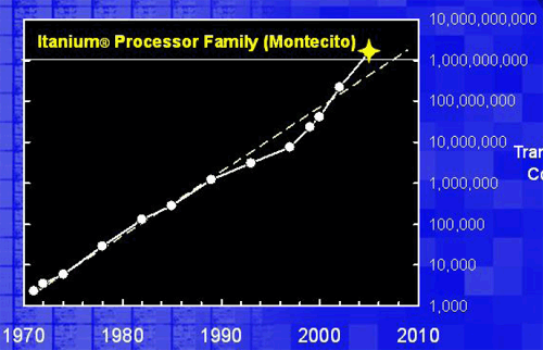
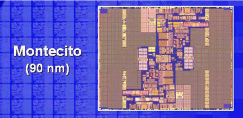
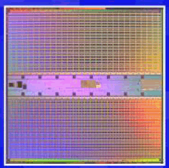
With the introduction of Montecito, Intel surpassed Moore's law very slightly with massive banks of cache. We will go into more detail about cache and SRAM in a little bit, but in the meantime we have an image of what the processor core actually looks like.
Next Generation Improvements
Of course, Montecito is already old news. 90nm is already old news. Strained silicon, low-k dialectrics and phase shifting lithography masks are also old news. Our interests belong to some of the technologies Intel discussed to bring the company out of the 90nm age in two years; into the 65nm interconnect era.
At AnandTech, we love roadmaps - particularly roadmaps with internal code names, wafer sizes and process technology. Stumbling into a development talk at the right time gave us a glimpse at Intel's 6 year plan for lithography.
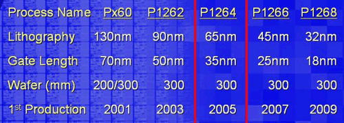
Intel positioned itself to ramp a new lithography generation every two years - currently the 90nm D1D in Hillsboro, Oregon, houses the development technologies for 2005's introduction of 65nm technology. Some of Intel's most promising technologies fit into a nice line graph plotting process size against time.
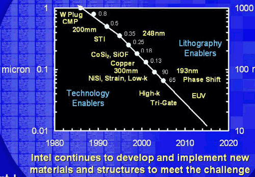
Technologies like strained silicon and low-k dialectrics are just first steps for Intel. We are going to give a small primer on as much of these technologies as possible.
Lithography
Moving to a 65nm transistor requires a 65nm lithography process. We are already seeing devices being built into silicon with features smaller than the wavelength of the light used in the lithography process. As it will be somewhere near 2009 before Intel has their EUV (13nm light wavelength) technology up and running, working with such small features requires some special masking tricks.
At this level, engineers must take into account the fact that light displays properties of both particles and waves. In order to create the situation where a particle of light has a high probability of hitting such a small section of photoresist covered silicon, special masking techniques need to be used to manipulate the wave.
Though it's not the same thing, anyone who has access to a laser can see how a light wave can be manipulated. Just take a piece of paper and cut two vertical slits that are close enough together so as to fit within the radius of the laser pointer beam. Find a dark room, stand a few feet from a wall, and shine your laser through the slits in the paper. What will be seen is a series of vertical lines which represent the interference pattern of the light waves passing through each slit. Well, that's the explanation if we don't try to talk about it on the quantum level.
Using similar properties exhibited by light (though not exactly the same as our example), Intel has devised technology they call Alternating Phase Shift Masks in order to etch extraordinarily small features into a silicon integrated circuit for 65nm fabrication.
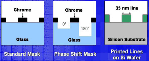
Moving to 32nm fabrication, we think Intel will be forced to move to EUV (both the process technology roadmap and the move to 13nm wavelength lithography will occur circa 2009). But until then, and even beyond, advanced masking techniques will enable photolithography to keep up with the ever decreasing size of transistors on silicon.
Silicon and Transistor Technology
Advances in lithography technology have only been half of the battle in fulfilling Moore's law. In fact, silicon and transistor technology itself has undergone radical changes in the last couple years (particularly with technology like strained silicon). Putting more transistors on a processor recently has had more to do with increasing cache size rather than increasing logic on the CPU. Advances in lithography and gate technology dramatically increase our density of other components such as SRAM - the building blocks of cache memory.
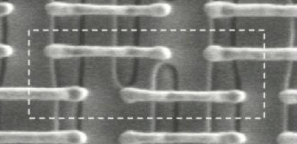
DRAM effectively utilizes one transistor per cell, allowing high densities but unfortunately operating at low speeds. SRAM utilizes six transistors per cell in a flip flop configuration, lowing density but allowing operation at several GHz. Below, Intel demonstrates a 110mm2 SRAM module with a 70Mbit capacity (over 500 million transistors). This is less than a modern BGA module can handle, but consider the SRAM module can operate several GHz faster than any DRAM module with ease.
You can see an actual SRAM cell in the image below. The white dash outlines a cell with an area about 0.57um2.
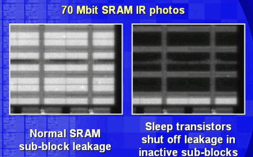
Simply designing more and more transistors on a chip does not make sense if thermal issues bog down the true capabilities of the processor. We spotted one new technology that did not receive a lot of attention during the presentations; the introduction of sleep transitors. Sleep transistors act as miniature controllers to an SRAM bank, throttling power during operating to reduce leakage. The sleep transistors themselves do not sleep, but rather the transistors they control do.
Further advances at Intel, like trigate transistors will essentially place transistor interconnects on a 3D grid instead of a 2D one - allowing for much higher densities without revamping lithography or gate size.
Intel already uses low-k dielectrics between their metal layers to reduce capacitance They use a Carbon Doped Oxide (CDO) for this, though they weren't specific about what oxide they are using for this. This will continue into 65nm, and strained silicon will see some slight revisions as well. Currently their silicon germanium (PMOS) and nickel silicide (NMOS) strained silicon gives about a 20% average improvement in transistor drive current, but Enhanced Strained Silicon (as they are calling it) promises a 30% average improvement.
At this point in time, Intel did not discuss exactly what makes their next step in strained silicon "enhanced", but they were fairly tight lipped about their original implementation before it hit the market.
Extensions of Moore's Law
Knowing all of the technical terminology and process information is helpful, but really all of these technologies and advances in production boil down to only a few basic elements that in turn affect Intel's implementation of Moore's law.
With process and lithography size shrinking, every processor family revision provides a 30% reduction in line length.
0.7x line length every 2 years
Adding more layers, decreasing line length and decreasing gate size allows for a 50% reduction in SRAM size every processor family revision.
0.5x SRAM size every 2 years
This conveniently falls in the pattern of processor introduction from Intel for several generations now. Prescott 2M (Pentium 4 6xx) will ship with 2MB L2 cache, Prescott (Pentium 4 5xx) debuted with 1MB L2 cache, Northwood had 512KB L2 and Willamette had 256KB. The 18 month revision between Banias and Dothan also demonstrated a double in cache size. The truth is, Moore's law is in no danger in fading anytime soon - particularly through 2009 where we can continue to expect SRAM sizes to decrease by 50% every two years; thus enabling Intel to place approximately twice as many transistors on a die. Technology like trigrate transistors may even expedite SRAM density with three dimentional gates.
And on that note, we'll end our coverage of the second day of IDF Fall 2004. We still have a few more stops to make, the show floor to cover, another keynote, and AMD to see. Hopefully we will be able to dig up more juicy tidbits of tantalizing tech news for all to feast on. Right now, its time to get in a little breakfast before the next busy day of meetings and sessions begins.


