Original Link: https://www.anandtech.com/show/1083
Intel's Centrino CPU (Pentium-M): Revolutionizing the Mobile World
by Anand Lal Shimpi on March 12, 2003 6:10 AM EST- Posted in
- Laptops
Looking at the way mobile CPUs have been developed in the past, it's very clear that this isn't the right way to solve the problem of producing a high performance, low power CPU.
AMD or Intel would simply take a desktop CPU, scale it down (in both frequency and voltage), make it go to sleep as much as possible and call it a mobile processor. This worked for a while when we were dealing with relatively low power desktop CPUs like the Pentium III, but take a look at the power requirements of a mobile Pentium 4 running at 2.4GHz and you'll quickly come to the conclusion that there has to be a better way.
Now look at AMD's plans with their mobile Athlon 64; in this case they're taking a server CPU that was already scaled down to be a desktop part and doing whatever it takes to make it a mobile processor.
Neither AMD nor Intel's approaches to mobile CPU and platform architecture will work, and it's very clear the reasons why; other than reducing clock speed and attempting to keep voltages as low as possible, the CPUs are still architecturally identical to their desktop counterparts. There are always going to be parts of the chip that aren't optimized for low power operation, making the CPU far from well designed for mobile applications. When the architects at AMD and Intel are designing their desktop or server processors, they aren't concerned with battery life on a notebook, and thus the vast majority of the decisions they will make will be insensitive to the needs of a mobile CPU.
Moving beyond the CPU, the chipset and rest of the platform are also taken directly from the desktop world. The North Bridge in today's notebooks is identical to what we see on desktops, and with the amount of traffic that goes through that chip, there's definitely a lot of wasted power.
The amount of inefficiencies in current mobile architecture is astounding when you think about it, and after today, you'll understand how they're all going to go away…
The History of Banias
The face of mobile computing actually changed a little over three years ago, when Intel announced a chip they were working on called Timna. Timna was designed to be a desktop CPU for a new market, the sub-$600 desktop PC segment. The CPU and platform were going to enable this by integrating the memory and graphics controllers onto the CPU's die itself. If you're curious as to why Intel is so adamant about not integrating a memory controller on die, the failure of Timna could be a strong case against the idea.
At the core, Timna was based directly on Intel's Pentium III but the entire processor, from the way the chip was laid out to the way it was packaged was optimized for cost. Wherever money could be saved, Intel's Israel design team managed to cut costs, and in doing so became intimately familiar with the Pentium III architecture. Much of the technology and cost saving techniques that were developed in Israel for Timna ended up being used by other groups at Intel in everything from desktop to server CPUs, so even the Pentium 4s we've got today have a little bit of Timna in them.
As we mentioned before, Timna was to feature an integrated memory controller, but at the time it was on the drawing board Intel still had delusions of grandeur about RDRAM being the future of all memory technology by 2001. The high price of RDRAM coupled with the lack of demand for such a low cost chip (OEMs weren't too happy with nonexistent profit margins on sub-$600 PCs), led to pulling the plug on Timna just after the chip was completed.
For Intel's Israel design team, the death of Timna was like the loss of a family member. A CPU that they had worked feverishly on for quite some time was now never going to make it to fruition; and the most painful part of it all, especially to an engineer, was that the Timna failure had absolutely nothing to do with the design of the chip, and everything to do with the outside factors that a design team cannot control.
Things were so bad for the Israel design team that when they were immediately summoned to begin work on a dedicated mobile processor, they were almost in a state of depression. How would you feel if your blood, sweat and tears were poured into something that just ended up a lost memory? Luckily, for the sake of the Israel design center and Intel's mobile computing plans, the Timna team didn't spend too much time mourning their loss and quickly began work on designing Intel's first truly mobile processor.
The design team looked at the Pentium 4's architecture and quickly concluded that it wouldn't be appropriate for a mobile microprocessor. An extremely long pipeline for a CPU designed to run at very high frequencies was not conducive to building a processor that could run within a 24W power envelope. There were some features that they could borrow from the Pentium 4, but for the most part, the NetBurst architecture was not one that could be considered as the basis for the CPU that would end up known internally as Banias.
One benefit the Israel design team had was their intimate experience with the P6 architecture; although the experience was mostly from a cost reduction and integration standpoint, both of those areas left the team with a solid understanding of the inefficiencies of the P6 core as well as what could be brought over into Banias unchanged.
What was born out of Timna's ashes and the extreme dedication/talent of Intel's Israel design team was a processor that can easily be classified as a Pentium III with a Pentium 4 bus, but wrongly so. What Banias ended up being, was the most interesting microprocessor architecture that we've ever seen…
Longer than a Pentium III, Shorter than a Pentium 4
The first thing that you'll notice about our coverage of the Banias' architecture is that the amount of detail we can provide you is sketchy at best. The reason being that Intel is guarding a great deal of what went into Banias very carefully, so carefully in fact that there are technologies that went into Banias that Intel is afraid to patent, because of the danger of the competition picking up on them through the patent filing.
You get your first dose of Intel's close guarded nature in regards to Banias with the talk of its integer/floating point pipelines. The chip itself has a longer pipeline than the Pentium III, but a shorter pipeline than the Pentium 4. The reason for this is simple; the Pentium III's architecture ended up topping out at just above 1.20GHz on a 0.13-micron process, but in order for Banias to fulfill Intel's desires for a high performing mobile CPU, they would need a higher clock speed. At the same time, remember our earlier discussion about the Pentium 4's pipeline being too long for the good of a mobile CPU. The end result? Something in between the Pentium III's 10-stage pipeline and the Pentium 4's 20-stage pipeline.
Intel wouldn't reveal the exact number of stages, nor what the individual stages are responsible for, but over time we will probably come across this information. For the purposes of this article, just know that the pipeline is longer than the P6 and shorter than NetBurst.
Remember that one of the downsides to having a long pipeline is the penalty incurred for a mispredicted branch. As we've discussed in our articles on the Pentium 4's NetBurst architecture, one of the approaches to improving superscalar microprocessor performance is to predict the path taken in a branch in the code being executed (e.g. choosing the outcome of an if-then statement without knowing whether the 'if' condition can be fulfilled).
Generally speaking, most branches can be correctly predicted, but it's what happens when a branch is incorrectly taken (or not taken) that performance suffers tremendously. In the case of a desktop CPU like the Pentium 4, a branch mispredict means that the entire pipeline must be flushed and execution will start over again, which means we've just wasted a good number of precious clock cycles. For a mobile CPU, the process is the same but now we're not only wasting clock cycles, we're also wasting battery power, which is a limited resource in the mobile world. Now can you begin to understand why a longer pipeline is undesirable in a mobile CPU?
By going with a pipeline that's longer than the Pentium III, the design team immediately brought it upon themselves to make sure that Banias doesn't suffer as much from a mispredicted branch. One way of reducing the penalty of a mispredicted branch is to use a trace cache, just like in the Pentium 4. A trace cache stores decoded micro-ops in their sequence of execution, meaning that in the event of a branch mispredict, the CPU can start later in the pipeline instead of having to go back to square one. The problem with a trace cache is that it eats up quite a few gates and is very power hungry, two things that kept it out of the Banias design.
Without a trace cache, the design team was forced to develop a more accurate branch predictor unit for the Banias core. Although beyond the scope of this article, Banias was outfitted with a branch predictor significantly superior to what was in the Pentium III. The end result was a reduction of mispredicted branches by around 20%.
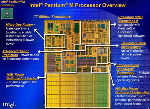
We have already discussed a couple of the other aspects of the Banias architecture from tidbits of information revealed at previous Intel Developer Forum conferences. The name of the game with Banias is efficiency, and thus the Israel design team introduced a technology called micro-ops fusion into the Banias core.
The idea behind micro-ops fusion is to bundle micro-ops (decoded instructions) together before sending them down the pipeline to the execution units. The idea behind micro-ops fusion is that the pipeline is not used unless a fixed number of micro-ops are ready to be sent down the pipe, thus the efficiency of the overall pipeline is improved. Obviously the downside to this approach is increased latency, but as you will see with a number of the design decisions behind Banias, the power savings enable higher overall performance at the end of the day.
Banias' dedicated stack manager is another power saving tool integrated into the Banias architecture that is designed to manage stack pointers and other stack-related data. Remember that stacks are used to store information about the current state of the CPU including data that cannot be kept in registers due to limits in the number of available registers, thus a dedicated manager can help performance considerably. As usual, whenever efficiency is improved power consumption is optimized which is the case with Banias here as well.
The combination of a very advanced branch predictor, micro-ops fusion and a dedicated stack manager make Banias a very interesting architecture. Despite having a 20 - 50% longer pipeline, Banias still maintains a significantly higher IPC than the Pentium III, which is not an insignificant achievement. Remember from our discussions about the Pentium 4 that IPC (Instructions executed Per Clock) is generally reduced by moving to a longer pipeline, but is made up for by the fact that longer pipeline architectures can reach higher clock speeds. With Banias, we have an architecture that already has a longer pipeline than the Pentium III, thus enabling higher clock speeds, all while boasting a higher IPC - you're in fact getting the best of both worlds with Banias.
In order to feed the higher IPC execution core, Intel outfitted the Banias with a 64-bit 100MHz quad-pumped FSB, identical in design to the Pentium 4's FSB. The Banias' FSB is even electrically compatible to the Pentium 4's FSB, which is why any Pentium 4 chipset is able to interface with the chip as we saw at IDF with this E7501/Banias setup:

If you're picking up on the fact that Banias is significantly different from the Pentium III, then you're on the right track…
Pentium III Execution Power
There's a difference between making a derivative microprocessor architecture and not re-inventing the wheel; we've already established that Banias is significantly different from the Pentium III, but the Israel design team didn't just synthesize the CPU from scratch in order to be genuinely different than the Pentium III.
Much like the Athlon 64 shares the same execution units as the Athlon XP, the Banias has the same execution unit layout as the Pentium III. This means that Banias features no more than 5 execution ports, significantly less than what we're used to seeing from the Pentium 4 for example.
By sticking with a relatively narrow execution layout, Intel continues to limit the power consumption of the Banias core; as our IPC comments from the previous section indicate however, the limited number of execution resources won't hold back performance. What the limited number of execution resources does mean however is that Hyper-Threading will not "work" on Banias.
Remember that Hyper-Threading works based on the idea that there are enough execution units in the Pentium 4 and enough pauses in the pipeline that there are execution units that remain idle during normal operation. With Banias' short pipeline, micro-ops fusion and relatively narrow architecture (read: lack of a large amount of execution units in parallel), Hyper-Threading won't find much use because of the lack of periods of idle execution.
So, no Hyper-Threading, big deal right? It would have been easy to shrug off if it hadn't been for Pat Gelsinger mentioning that "threading" was the future of Intel's microprocessor design efforts at dinner a year ago. By "threading" Pat was referring to being able to execute multiple threads on a single microprocessor, the most familiar way these days being through the use of Hyper-Threading, a technology that dispatches multiple instruction streams from different threads through the same pipeline and down to the same execution units.
We've already discussed why this won't work for Banias, so what will? Although it will be a while before we see this, the idea would be to have a multi-core die, with some sharing of execution units and/or caches in order to keep die size down to a minimal. We won't get too off track with talking about the future of Banias, but for now it's something to keep in the back of your mind for the years to come…
Banias' Caches
We mentioned at last year's Fall IDF that Banias would be a 0.13-micron processor composed of no less than 77 million transistors. Almost half of the Banias die is reserved for cache and as you can expect, the cache is nothing normal.
Banias is outfitted with a 64KB L1 cache, twice the size of the L1 found on the Pentium III. The L1 is split into a 32KB data cache and a 32KB instruction cache; as we mentioned before, the gate-hungry trace cache was rejected as an option for a mobile CPU although it would have reduced branch mis-predict penalties.
What's most impressive about Banias' caches is its 1MB on-die L2 cache. Not only did the Israel design team carefully design the transistors that make up the gates within the cache to maximize power savings, but they also changed the way data is actually accessed within the cache. Banias employs an 8-way set associative L2 cache, and normally in such a cache when one of the "ways" is selected, the entire block is selected. With Banias, each "way" is further split into quadrants so that when one is selected, a separate multiplexer selects which quadrant the necessary data is located in and only activates that part of the cache. The end result is that much less of the power hungry L2 cache is consuming battery life, which helps extend that battery life significantly.
Out of all of the transistors in a CPU, those dedicated for cache are generally the most power hungry, and thus keeping them inactive as much as possible helps tremendously in reducing power consumption. Of course the downside to this approach is that cache accesses now take a little longer, but the power savings are significant enough to make up for the performance deficit by going to a larger cache - which is why Banias is able to have such a large cache and still be relatively low on the power consumption scale.
The higher latency of the cache is masked by the fact that a 1MB L2 cache improves overall system performance enough to hide the majority of the latency hit.
Hitting those high clocks
Quite possibly the most interesting part of the way Banias was designed, relates to the processor's clock speeds and what it took to achieve them. As we've already mentioned, the CPU features a longer pipeline than the Pentium III which does help it hit higher clocks, but where does the limit exist?
In the course of designing a processor, you will eventually discover that there are certain speed paths in your CPU that will run either faster or slower than your target clock speed. If you run into paths that run slower than your target clock speed, you're in trouble, since it means that you won't be able to reach the clocks you were hoping to without some sort of a redesign. In most cases, if you find that a path is running faster than your target clock speed (e.g. finding a path capable of running at 2.4GHz on a chip with a 1.6GHz target clock speed) then you're in a very good situation, as it means that there are parts of your chip that have fairly high ceilings. For the Israel design team however, this wasn't the case.
The design team actually went in and slowed down paths that were running above Banias' target clock frequencies, because if a path is able to run faster than it should, it means that you're wasting power. The benefit of this is an even more power efficient microprocessor, but the downside is a microprocessor that has a clear clock frequency wall.
It is unclear what the frequency wall is for the current 0.13-micron Banias, but it is very clear that one exists. We'd hypothesize that the wall is somewhere around 2GHz, but what happens afterwards? The Israel design team couldn't deliver on all of the promises of the most efficient and high performing mobile CPU around without sacrificing frequency headroom, so instead of depending on the architecture to enable higher frequencies, the design team turned to Intel's manufacturing.
The idea is that by the time the core hits its frequency limit, a smaller manufacturing process with faster transistors will be ready for transitioning to. For this year, assuming that Intel's 90nm transition continues as planned, the situation isn't all that risky, but looking forward, there is a big risk with this sort of an approach. From Intel's perspective however, there's not much else that could have been done if you want to have the absolute best mobile CPU possible.
In the end, placing faith in Intel's manufacturing process isn't a bad bet, but it is a risk that Intel's competition would not take simply because they lack the resources to potentially fail.
Productizing Banias - Introducing the Pentium-M
For those of you that still believe microprocessor architectures are decided upon by marketing folks first and then handed off to engineers to make, Banias should be all the proof necessary to convince you otherwise.
Intel's Pentium M Processor
The core is clearly not designed for high clock speeds and thus provided Intel's marketing with a very difficult job. How do you explain to end users that there's a new mobile processor on the market that is faster than a Pentium 4 clock for clock, and because of its high IPC it is actually faster than most of the higher clocked Pentium 4s?
Intel's marketing team came up with the idea of moving the focus away from the processor itself, and over to the entire mobile package - CPU, chipset and wireless adapter. Intel branded this package of three components as Centrino, with hopes that end users would walk into a store and request a Centrino laptop, instead of a xxGHz laptop.
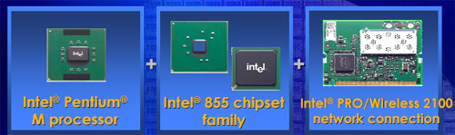
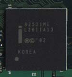
While we'll talk about the other parts of the Centrino architecture what we've been focusing thus far on has been the CPU itself, which has been going by the codename Banias for years now. The final name of Banias is the Pentium-M and today is available in 6 different flavors; each of the Pentium-M chips have the exact same features, cache sizes, etc… and only differ according to operating frequency and voltages:
|
-
|
Frequency
Performance/Battery Mode |
Voltage
|
Thermal
Design Power
|
| Pentium-M 1.60 |
1.60GHz/600MHz
|
1.48V/0.96V
|
24.5W
|
| Pentium-M 1.50 |
1.50GHz/600MHz
|
1.48V/0.96V
|
24.5W
|
| Pentium-M 1.40 |
1.40GHz/600MHz
|
1.48V/0.96V
|
24.5W
|
| Pentium-M 1.30 |
1.30GHz/600MHz
|
1.39V/0.96V
|
22.0W
|
| Low Voltage Pentium-M 1.10 |
1.10GHz/600MHz
|
1.18V/0.96V
|
12W
|
| Ultra Low Voltage Pentium-M 900 |
900MHz/600MHz
|
1.00V/0.84V
|
7W
|
As you can gather by the table above, the Pentium-M features the same SpeedStep technology that we've seen from previous Intel CPUs. On battery power, the CPU will drop to a noticeably lower clock speed (600MHz in the case of all first generation Pentium-M CPUs). The difference between the Pentium-M's power management and other mobile Intel CPUs is mainly in the way sleep states are handled; whereas conventional mobile CPUs put various parts of the core to sleep when idle, the Pentium-M starts out in sleep mode and parts of it are woken up when necessary. Once again, the downside is that it takes a few clock cycles longer to get the appropriate units to wake up, but the power savings are non-trivial, and thus enable higher performance in the end by allowing for features like a 1MB on-die L2 cache or a higher clock speed.
Power Saving Chipsets - 855PM & 855GM
One of the things we talked about in the introduction was the problem of using desktop chipsets for mobile environments. With Centrino, the Israel design team went in and applied their power-optimizing engineering techniques to the 845 DDR chipset.
One such technique is the way the chipset/CPU handle the FSB interface; on conventional mobile CPUs, when the CPU issues a read request, the read buffers on the CPU are active from the moment the request was sent from the CPU. However, if you look at the fact that the read buffers are not actually being used until the data being requested by the CPU is finally retrieved from memory then you'll realize that this isn't the best way of doing things.
The Centrino approach makes sense and is quite simple; keep in mind that the majority of the Pentium-M starts out in a sleep state, including the read buffers on its FSB interface. When a read request is sent from the Pentium-M CPU to the MCH (Memory Controller Hub aka North Bridge) the read buffers remain asleep, they don't wake up until the data is finally starting to be retrieved from main memory and is being sent to the MCH's buffers before a signal is sent from the chipset to the CPU instructing the CPU to power up the buffers. As is the case with most of the decisions behind the Centrino platform, the tradeoff here is between latency and power; sacrificing a bit of performance in the form of added latency ends up being worth the gain in power savings.
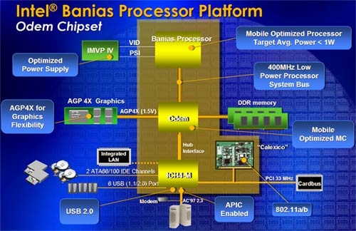
There are two chipsets being launched with the Pentium-M processor as a part of the Centrino mobile architecture - the 855PM and 855GM. Feature-wise, both 855 chipsets are essentially highly power optimized versions of the 845 chipset. They both feature a 64-bit DDR266 memory interface and AGP 4X support, but don't let their looks deceive you, the chipsets are significantly different from the 845. Just like the Pentium-M is far from a Pentium III, the 855 is far from an 845 as it consumes less than 1/2 the power of the 845 chipset.
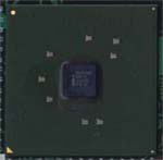
The 855PM MCH
Note that because of the low power consumption, cooling isn't necessary on the 855PM MCH.
The difference between the 855PM and GM is that the GM includes a power optimized version of Intel's 845G graphics core, while the 855PM has no integrated graphics.
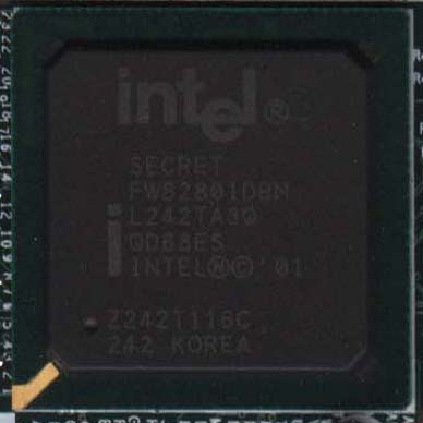
The ICH4-M
Both the 855PM and GM use a new ICH as well, ICH4-M. This particular ICH has deeper sleep states than what we're used to, but the optimizations are no where near as in depth as what we've seen on the CPU/MCH ends. The feature set of ICH4-M is identical to the desktop ICH4.
Wireless
The third and final piece of the Centrino puzzle is Intel's PRO/Wireless 2100 card. Notebook manufacturers must use this card (along with an 855 chipset and a Pentium-M CPU) in order to be able to call their notebook a Centrino system.
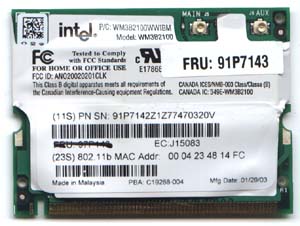
The benefit of being able to brand your notebook Centrino is that the manufacturer now gets access to Intel's marketing dollars in helping to sell their platforms. This effectively keeps other chipset makers out of Centrino notebooks and moves everyone towards Intel wireless solutions.
Intel's Wireless MAC
Intel's eventual goal is to integrate a 802.11b/g MAC into their MCH, meaning that soon enough you won't have a choice for what wireless MAC to use (although OEMs will be able to pick and choose PHYs), so this marketing strategy is more of a short term guarantee that manufacturers will be forced to use Intel's PRO/Wireless solution.
Pricing
The OEM pricing for Centrino bundles (CPU + Chipset + PRO/Wireless controller) is as follows:
|
-
|
Centrino
Package Price
|
| Pentium-M 1.6GHz |
$720
|
| Pentium-M 1.50GHz |
$506
|
| Pentium-M 1.40GHz |
$377
|
| Pentium-M 1.30GHz |
$292
|
| Low Voltage Pentium-M 1.10GHz |
$345
|
| Ultra Low Voltage Pentium-M 900MHz |
$324
|
The Test
For this review we used FIC's Centrino for our Pentium-M 1.5GHz system, and the IBM T40P for the 1.60GHz Pentium-M system.
|
|
Windows
XP Professional Test System
|
||||
|
|
Hardware
|
||||
|
Dell
Latitude D800
|
FIC Centrino | IBM T40 | IBM T40P |
Desktop
System
|
|
| CPU(s) |
Pentium
M 1.6GHz
|
Pentium
M 1.5GHz
|
Pentium
M 1.5GHz
|
Pentium
M 1.6GHz
|
Pentium
4 2.4GHz
|
| Motherboard(s) |
Dell
855PM
|
FIC
855PM
|
IBM
855PM
|
IBM
855PM
|
Intel
D845EBT 845E
|
| Memory |
512MB
PC2100
|
512MB
PC2100
|
256MB
PC2100
|
512MB
PC2100
|
512MB
PC2100
|
| Hard Drive |
40GB
5400RPM
|
30GB
4200RPM
|
40GB
5400RPM
|
40GB
5400RPM
|
IBM
Deskstar DPTA-372050 20.5GB 7200 RPM
|
| CDROM |
CD-RW/DVD
|
CD-RW/DVD
|
CD-RW/DVD
|
CD-RW/DVD
|
Philips
48X
|
| Video Card(s) |
NVIDIA
GeForce4 4200 Go 64MB DDR
|
Integrated
855PM
|
ATI
Mobility Radeon 7500
|
ATI
Mobility FireGL 9000 64MB DDR
|
ATI
Radeon 9000 Pro 64MB
NVIDIA GeForce4 Ti 4200 128MB |
| Ethernet |
Onboard
Intel Gigabit
|
Onboard
Intel Pro/100VE
|
Onboard
Intel Gigabit
|
Onboard
Intel Gigabit
|
Linksys
LNE100TX 100Mbit PCI Ethernet Adapter
|
|
|
Software
|
||||
|
Operating System |
Windows XP Professional SP1 |
||||
| Video Drivers |
NVIDIA
42.56
(latest available for Dell) |
Intel
6.13.01.3460
|
ATI
6.13.10.6278
(latest available for IBM) |
ATI
7.79.7.3 (latest available for IBM)
|
ATI
Catalyst 3.1
NVIDIA 41.09 |
|
|
Benchmarking Applications
|
||||
|
Bapco
SysMark 2002 |
|||||
Content Creation Performance
In order to measure Content Creation performance we used Multimedia Content Creation Winstone 2003 and Internet Content Creation SYSMark 2002. First we'll start off with the Winstone benchmark, which is best described by its creators at Veritest:
Multimedia Content Creation Winstone is a system-level, application-based benchmark that measures a PC's overall performance when running top, Windows-based, 32-bit, multimedia content creation applications on Windows 2000 (SP2 or higher), Windows 98, Windows ME, and Windows XP. Multimedia Content Creation Winstone 2003 uses the following applications:
Adobe® Photoshop® 7.0
Adobe® Premiere® 6.0
Macromedia® Director 8.5.1
Macromedia® Dreamweaver 4
Microsoft® Windows MediaTM Encoder 7.01.00.3055
Netscape® 6.2.3
NewTek's LightWave® 7.5
Sonic Foundry® Sound Forge® 6.0Following the lead of real users, Multimedia Content Creation Winstone 2003 keeps multiple applications open at once and switches among those applications. Multimedia Content Creation Winstone 2003 is a single large test that runs the above applications through a series of scripted activities and returns a single score. Those activities focus on what we call "hot spots," periods of activity that make your PC really work--the times where you're likely to see an hourglass or a progress bar.
|
Keeping in mind that the Pentium III had a higher IPC than the Pentium 4, and also remembering that the Pentium-M features a significantly higher IPC than the Pentium III, it's no surprise that a 1.6GHz Pentium-M is able to outperform the fastest Pentium 4-M CPU (2.40GHz) and come within striking range of a desktop 2.66GHz Pentium 4. The 1.5GHz Pentium-M is faster than a 2GHz Pentium 4, and on the heels of a 2.2GHz Pentium 4.
|
Internet Content Creation SYSMark 2002 is much more optimized for the Pentium 4's architecture, which is why we find the two Pentium-M processors at the bottom of this chart. Overall content creation performance should be somewhere in between what we see here and what we saw in Content Creation Winstone 2003. One thing is for sure though, the Pentium-M at 1.6GHz is significantly faster than the Pentium 4-M at 1.6GHz.
General Usage Performance
Although not as performance-critical as content creation applications, it is the set of every day applications like Office and other general usage programs that the majority of users find themselves interacting with the most.
We start with VeriTest's Business Winstone 2002:
The Business Winstone tests are "market-centered" tests. Business applications are the popular applications employed by most users every day.
Five Microsoft Office 2002 applications (Access, Excel, FrontPage, PowerPoint, and Word)
Microsoft Project 2000
Lotus Notes
WinZip 8.0
Norton AntiVirus
Netscape Communicator
|
Integer applications are very branch intensive and thus the Pentium-M's shorter pipeline and well balanced branch predictor (balanced for the architecture) give the 1.6GHz Pentium-M the title of the fastest mobile processor in Business Winstone 2002. Not only can the Pentium-M outperform the fastest Pentium 4, but it also comes out ahead of the 2.66GHz Pentium 4, even despite its higher speed FSB (533MHz vs. 400MHz).
|
We close off with some more office performance scores; this time around, the Pentium-M comes in neck and neck with the 2.66GHz Pentium 4 - a desktop CPU.
Because of the difficulty in putting together a good desktop vs. mobile graphics comparison, we've limited our performance tests here to 2D-only. For gaming performance of the Pentium-M, take a look at our Centrino Notebook Roundup.
Final Words
If you've read every word we've written about Centrino and the technology behind it and are impressed, then you haven't seen anything yet. The architecture and technology behind the platform goes far beyond what we're able to print, but the main point to convey is that the Pentium-M is not a Pentium III and not a Pentium 4, it's something very new and very different.
The approach Intel undertook with the Pentium-M is one that would be difficult for their competition (mainly AMD) to duplicate. It requires dedicating an entire design team to a project that will be taking significant risks and will be relying on perfect execution on the manufacturing side of things to meet product cycles. The sort of commitment Intel made with the Banias project required an incredible amount of resources, and put those resources at very high risk of being lost should anything have gone wrong. Maybe it was the passion that was burning within the hearts of the Israel design team or the desire to show Intel corporate what the team was capable of, but Banias was the first and only chip in Intel's history that was no more than 8 days late.
The future of the chip is also quite bright; there are a few tweaks that didn't make it into Banias that will be present in its 90nm successor known as Dothan by the end of this year. Dothan should be able to ramp frequencies up even higher, while providing an even larger 2MB L2 cache as has been leaked previously.
When looking at the present, the 1.6GHz Pentium-M is comparable to a Pentium 4-M 2.2/2.4GHz, with the 1.5GHz Pentium-M falling somewhere in the 2.0 - 2.2GHz range. For business/office applications, the Pentium-M is unbeatable, clearly outperforming the fastest mobile Pentium 4 at 2.40GHz. When dealing with games and media encoding applications, the Pentium 4 will be faster, but by no means will it be able to offer the battery life of a Pentium-M based system.
For the foreseeable future, the Pentium 4-M and Pentium-M will coexist, but the Pentium 4-M will be mostly restricted to the highest end desktop replacement notebooks, where battery life isn't as big of a concern. For all other segments, the Pentium-M and the Centrino platform will do their job better than the Pentium 4 ever could. The ultra low-volt Pentium-M processors will finally make high-performance Tablet PCs a reality and will be a good successor to current ULV Pentium III notebook solutions.
In the end, the Pentium-M and the Centrino platform in general will do more for mobile computing than any single technology we've seen in the past. If you want an idea of just how big of an impact they're having already, take a look at our roundup of the first four Centrino/Pentium-M based systems we were able to get our hands on in time for launch...


