Original Link: https://www.anandtech.com/show/72
When choosing a motherboard, you must deal with quite a few factors, expansion slots, processor support, speed, stability, and much more, however the root of most of these factors is the chipset the motherboard is designed around. Ever wonder what makes the FIC PT-2007 cache only 64MB of RAM and what makes the FIC PA-2007 cache > 64MB? Not the design of the motherboard, not more experienced engineering, rather the features of the chipset found in each motherboard.
Today there are a number of manufacturers contributing to the chipset market, currently Intel holds the lead with their amazing Triton series of chipsets, and more recently with their P6 line of chipsets, dubbed the 440 and 450 series for desktop and server systems respectively. However, in recent times, VIA Technologies has caught up to Intel's glory and has sought to take a chunk of the tasty market pie. Of course there are other competitors however the main two competing for the title of best chipset manufacturer are undoubtedly Intel and VIA. Who is the winner, where does the competition stand? Keep on reading to find out...
| Socket-7 Chipsets | Slot-1 Chipsets | ||||
| Acer Labs Inc (ALi) | Intel | ||||
| Aladdin IV | Aladdin V | 440FX | 440LX | ||
| 440BX | 440GX | ||||
| Intel | VIA | ||||
| 430FX | 430HX | Apollo Pro | |||
| 430VX | 430TX | ||||
| Silicon Integrated Systems (SiS) | |||||
| 5571 | 5597/5598 | ||||
| VIA | |||||
| VP1 | VP2/97 | VP3 | MVP3 | ||
| VPX/97 | VXPro | ||||
You may assume that the TXPro chipset is also a product of VIA Technologies' efforts, however it seems like ALi (a division of Acer) has taken it upon themselves to produce this low cost TX Imitation. ALi, recently rumored to be working closely with AMD on a K6 chipset with support for a 133MHz bus speed as well as a 66MHz PCI bus speed, hasn't really been at the top of the chipset industry much since Intel's devastating release of the original Triton chipset.
What ALi hoped to accomplish with the TXPro was exactly what the VXPro was intended to do, offer a low cost solution to take a chunk of Intel's sales. With most TXPro based motherboards offering stable performance at the 75 and 83.3MHz bus speeds, and going for about $60 why wouldn't you want a TXPro motherboard? The chipset itself is quite competitive although I wouldn't compare the scores of a TXPro board to a genuine TX board like the ABIT AX5 or the Shuttle HOT-569, however if you don't need the absolute best of the best, then you may want to consider this chipset.
The TXPro is closely based on ALi's Aladdin IV/+ chipset which is amazingly enough (yeah right...) a lot like Intel's TX chipset with a few extra features, hence the name TXPro. One of the major advantages of the TXPro over the Intel TX chipset is the fact that it DOES support ECC DRAM, although it can still only cache the first 64MB of RAM installed when using an 8-bit Tag RAM. Motherboard manufacturers have the option of using an 11-bit Tag RAM to expand the cacheable memory area to 512MB, however doing so does raise the cost...a sacrifice most manufacturers that opt to go with the Aladdin IV won't make. An interesting feature the Aladdin IV boasts, which remains undocumented in most TXPro motherboards, is that the chipset features internal L2 cache Tag bits, therefore reducing cost, and also virtually eliminating any problems you might have experienced with running your motherboard at a higher bus frequency as a direct result of the L2 cache.
If you're looking for a cheap motherboard with some advanced features only found in more expensive models, give a TXPro based board a try...but beware, you aren't getting the world's most compatible product when you buy a TXPro board, just a reminder, you get what you pay for in this industry.
| ALi TXPro (Aladdin IV) Chipset | ||
| Common Name | TXPro | |
| Chipset Packaging | Number of chips | 2 (M1531 & M1533) |
| Packaging Type | 2 x 328-pin BGA | |
| CPU Support | Number of CPUs | 1 |
| AMD CPUs Supported | K5, K6 | |
| Cyrix CPUs Supported | 6x86 (M1), 6x86MX (M2) | |
| Intel CPUs Supported | Pentium, Pentium MMX | |
| Cache | Type | Synchronous Pipeline Burst Cache |
| Maximum Supported Size | 1024KB | |
| Maximum Cacheable DRAM Area | 64MB (8-bit Tag RAM) 512MB (11-bit Tag RAM) |
|
| Memory | Maximum DRAM Supported | 1GB (8 RAS Lines) |
| BEDO DRAM Read Timings (66MHz) | N/A | |
| EDO DRAM Read Timings (66MHz) | 5-2-2-2 | |
| FPM DRAM Read Timings (66MHz) | 5-3-3-3 | |
| SDRAM Read Timings (66MHz) | 5-1-1-1 | |
| Data Path to Memory | 64-bits | |
| ECC Support | Yes | |
| Hard Disk Controller | Chip | M1533 |
| Busmastering Support | Yes | |
| UltraDMA Support | Yes | |
| Max. Theoretical Transfer Rate | PIO Mode 5/DMA Mode 3 (33.3MB/S) | |
| PCI Interface | Supported PCI Bus Speeds | 25, 30, 33 MHz |
| Concurrent PCI | Yes | |
| Async. PCI Bus Speed | Yes | |
| PCI Specification | 2.1 (66 MHz max.) | |
| Power Management | PC97 Compliance | Yes |
| Suspend to Disk | Yes | |
| HDD Power Down | Yes | |
| Modem Wakeup | Yes | |
| System Suspend | Yes | |
| Video | AGP Support | No |
| Unified Memory Architecture | No | |
| Peripheral Support | USB Support | Yes |
| Plug and Play Port | Yes | |
| Write Buffers | CPU-to-DRAM | 16 QWords |
| CPU-to-PCI | 6 DWords | |
| PCI-to-DRAM | 36 DWords | |
| Officially Supported Bus Speeds | 50, 60, 66, 75, 83 MHz | |
| Unofficially Achieved Bus Speeds | Unknown | |
When AMD announced that they were looking for a candidate for the "official" Super7 Chipset (Socket-7 + AGP + 100MHz Frontside Bus) the market never expected Acer Labs (ALi) to be a viable candidate. Originally best known for their low cost Aladdin IV chipset found in most PC Chips motherboards, ALi was never much of a contender in the Chipset Industry taking a back seat to the duel of Intel and VIA. For once, the Socket-7 Chipset Market is the platform for a 4-way war of chipsets between Intel's 430TX, VIA's VP3 (and MVP3), SiS' 5591, and now, ALi's Aladdin V. What makes the Aladdin V so special? Quite a few things.
First of all, the Aladdin V meets all of the requirements to be a Super7 chipset, it supports the Accelerated Graphics Port, all current Socket-7 processors including AMD's upcoming K6-3D, and, the most sought after feature in a Socket-7 chipset, support for a 100MHz Frontside Bus. A combination of meeting these requirements, the extremely large cacheable memory area of the chipset, and a feature-set that puts Intel's TX Chipset to shame makes the Aladdin V chipset appear to be the king of the Socket-7 arena...or at least a contender for the throne.
The Aladdin V, in theory can accept up to 1GB of RAM, all cacheable. Doing so would put outstanding amounts of stress on the Bus, especially when using the 100MHz bus speed, so expect Aladdin V motherboards to feature no more than 3 DIMM slots. One of the most important features the Aladdin V chipset boasts is the internal L2 cache the chipset features, more specifically the M1541 chip has an integrated 16K x 10-bit Tag RAM as well as 16K x 2 L2 cache SRAM, both of which decrease cost and increase performance somewhat. The most important reason for including the Tag RAM on chip is to make using the 100MHz bus speed possible. The 100MHz Bus Frequency puts a heavy strain on the L2 cache, and tests have shown that without fast L2 cache & a capable Tag RAM chip (6ns or faster) the 100MHz bus speed has the potential to become quite erratic. By placing the Tag RAM on the chipset ALi eliminates the possibility of the L2 cache or chipset as being the limiting factor in making use of the 100MHz bus speed. Leaving your CPU, and Memory since the Aladdin V supports a Pseudo Synchronous PCI/AGP Bus to keep the PCI bus speed at or around the 33MHz marker, and the AGP bus at or around the 66MHz point.
The deep buffers between the CPU and DRAM interfaces should keep performance of the Aladdin V on par with or above that of all Socket-7 motherboards based on Intel chipsets, using the 100MHz bus speed the Aladdin V should be able to remove the Intel TX chipset from the picture as a possible competitor when dealing with performance.
UltraDMA, PC97 Compliance, and Advanced Power Management support are among the now standard features that ALi brings to the table with their Aladdin V, making it a very promising chipset...shortly you'll begin to see the first Aladdin V motherboards make their way into the mainstream market, then we can truly decide whether or not this chipset lives up to the hype.
| ALi Aladdin V Chipset | ||
| Common Name | Aladdin V | |
| Chipset Packaging | Number of chips | 2 (M1541 & M1543) |
| Packaging Type | 1 x 456-pin BGA (M1541), 1 x 328-pin BGA (M1543) | |
| CPU Support | Number of CPUs | 1 |
| AMD CPUs Supported | K5, K6, K6-3D | |
| Cyrix CPUs Supported | 6x86 (M1), 6x86MX (M2) | |
| Intel CPUs Supported | Pentium, Pentium MMX | |
| Cache | Type | Synchronous Pipeline Burst Cache |
| Maximum Supported Size | 1024KB | |
| Maximum Cacheable DRAM Area | 512MB (10-bit Tag RAM -
512KB L2) 1GB (256KB L2) |
|
| Memory | Maximum DRAM Supported | 1GB (8 RAS Lines) |
| BEDO DRAM Read Timings (66MHz) | N/A | |
| EDO DRAM Read Timings (66MHz) | 5-2-2-2 | |
| FPM DRAM Read Timings (66MHz) | 5-3-3-3 | |
| SDRAM Read Timings (66MHz) | 3-1-1-1 | |
| Data Path to Memory | 64-bits | |
| ECC Support | Yes | |
| Hard Disk Controller | Chip | M1543 |
| Busmastering Support | Yes | |
| UltraDMA Support | Yes | |
| Max. Theoretical Transfer Rate | PIO Mode 5/DMA Mode 3 (33.3MB/S) | |
| PCI Interface | Supported PCI Bus Speeds | 25, 30, 33 MHz |
| Concurrent PCI | Yes | |
| Async. PCI Bus Speed | Yes (Pseudo Synchronous) | |
| PCI Specification | 2.1 (66 MHz max.) | |
| Power Management | PC97 Compliance | Yes |
| Suspend to Disk | Yes | |
| HDD Power Down | Yes | |
| Modem Wakeup | Yes | |
| System Suspend | Yes | |
| Video | AGP Support | Yes |
| Unified Memory Architecture | No | |
| Peripheral Support | USB Support | Yes |
| Plug and Play Port | Yes | |
| Write Buffers | CPU-to-DRAM | 32 QWords |
| CPU-to-PCI | 6 DWords | |
| PCI-to-DRAM | 48 DWords | |
| Officially Supported Bus Speeds | 50, 60, 66, 75, 83, 100 MHz | |
| Unofficially Achieved Bus Speeds | Unknown | |
Intel made the first major jump into the chipset industry with the release of their very successful 430FX Chipset, commonly known as the Intel Triton I or simply the FX Chipset.
Although now impractical for most applications, the 430FX was a very strong performer and competitor during its time. Most of the original Triton's success came courtesy of its memory and disk controllers. The 430FX was the very first Intel chipset designed to officially support the, at the time, newest memory standard, Extended Data Out Dynamic Random Access Memory (EDO DRAM for short). This gave users, for the first time, the chance to get a taste of the high end market without shelling out the big bucks. The combination of high speed EDO DRAM with the advanced architectural features the original Pentium [Classic] had to offer made the FX Chipset ideal for most users, and that reign continued for quite some time as there was no real demand to replace the 430FX.
The Triton I also introduced the idea of using a technique called Busmastering to the enhanced IDE controller, which is the part of the chipset used for controlling EIDE peripherals (i.e. HDDs). These Busmastering capabilities were provided by the PIIX controller which in theory, and in practice, speeds up hard disk data transfers on either EIDE channel by granting EIDE peripherals certain SCSI like qualities. In spite of its strengths in memory support and hard disk access, the original Triton chipset had quite a few shortcomings. Although the 430FX allowed the use of up to 512KB of secondary Level 2 Pipeline Burst Cache (PBSRAM) and 128MB of RAM the chipset itself fails to cache any memory beyond the first 64MB. This posed a major problem to high end users expecting the maximum performance and power out of their systems.
Being the first member of the Triton family of chipsets the 430FX does not natively support any enhanced video features or caching schemes, the first introduction of such features came almost 2 years later with the release of the Intel 430VX chipset and its support for the Unified Memory Architecture. Power saving also isn't much of a strongpoint of the 430FX chipset, it fully supports the bare minimum requirements to be used in an "energy efficient" system, however features like Instant-On, and Suspend to Disk aren't included in this category. The performance of the original Triton isn't all that bad, however it is quite pointless to build a 430FX based system now since the torch has already been passed to the better designed 430HX and 430TX chipsets.
| Intel 82430FX Chipset | ||
| Common Name | Triton I | |
| Chipset Packaging | Number of chips | 3 (82437FX, 82438FX, 82371FB) |
| Packaging Type | 1 x 208-pin QFP; 2 x 100-pin QFP | |
| CPU Support | Number of CPUs | 1 |
| AMD CPUs Supported | N/A | |
| Cyrix CPUs Supported | N/A | |
| Intel CPUs Supported | Pentium | |
| Cache | Type | Asynchronous/Synchronous Pipeline Burst Cache |
| Maximum Supported Size | 512KB | |
| Maximum Cacheable DRAM Area | 64MB | |
| Memory | Maximum DRAM Supported | 128MB |
| BEDO DRAM Read Timings (66MHz) | N/A | |
| EDO DRAM Read Timings (66MHz) | 7-2-2-2 | |
| FPM DRAM Read Timings (66MHz) | 7-3-3-3 | |
| SDRAM Read Timings (66MHz) | N/A | |
| Data Path to Memory | 64-bits | |
| ECC Support | No | |
| Hard Disk Controller | Chip | PIIX (82371FB Controller) |
| Busmastering Support | Yes | |
| UltraDMA Support | No | |
| Max. Theoretical Transfer Rate | PIO Mode 4/DMA Mode 2 (16.6MB/S) | |
| PCI Interface | Supported PCI Bus Speeds | 25, 30, 33 MHz |
| Concurrent PCI | No | |
| Async. PCI Bus Speed | No | |
| PCI Specification | 2.0 (66 MHz max.) | |
| Power Management | PC97 Compliance | No |
| Suspend to Disk | No | |
| HDD Power Down | Yes | |
| Modem Wakeup | No | |
| System Suspend | No | |
| Video | AGP Support | No |
| Unified Memory Architecture | No | |
| Peripheral Support | USB Support | No |
| Plug and Play Port | Yes | |
| Write Buffers | CPU-to-DRAM | 4 QWords |
| CPU-to-PCI | 4 DWords | |
| PCI-to-DRAM | 12 DWords | |
| Officially Supported Bus Speeds | 50, 60, 66 MHz | |
| Unofficially Achieved Bus Speeds | None | |
With Intel's newly found place in the chipset industry they decided to improve on their already outstanding design by creating the long awaited successor to the 430FX chipset. This time around, Intel focused their attention more on high end speed and power rather than simply "getting the job done". It is this attitude that gave the 430HX chipset the leading edge over the rest of the market for quite some time, however motherboard manufacturers were reluctant to charge the outstanding cost of the HX chipset. Some manufacturers decided to cut corners by including a degraded Tag RAM chip which only enables the first 64MB of RAM to be cached instead of the Maximum 512MB.
The Performance of the Triton II is still quite competitive today with most higher end processors and configurations. Unlike the original triton, this successor has the ability to support dual CPUs as well as ECC DRAM and USB. The EDO timings on the HX Chipset are considerably faster than those on the FX chipset which means you can expect a greater overall memory performance with the HX Chipset, especially if using over 64MB of RAM, the cacheable limit of the FX. The HX Chipset also extends CPU compatibility to IBM/Cyrix as well as AMD and Intel which makes it a better competitor even today. Its PIIX3 BMIDE Controller is considerably faster than the PIIX controller found in the FX chipset, however it still doesn't support the UltraDMA specification. The Triton II was also the first chipset to even unofficially support the 83.3MHz bus frequency now very common in most decent motherboards today.
| Intel 82430HX Chipset | ||
| Common Name | Triton II | |
| Chipset Packaging | Number of chips | 2 (82439HX System Controller, 82371SB) |
| Packaging Type | 1 x 324-pin BGA; 1 x 208-pin lead QFP | |
| CPU Support | Number of CPUs | 2 |
| AMD CPUs Supported | K5, K6 | |
| Cyrix CPUs Supported | 6x86 (M1), 6x86MX (M2) | |
| Intel CPUs Supported | Pentium, Pentium MMX | |
| Cache | Type | Pipeline Burst Cache |
| Maximum Supported Size | 512KB | |
| Maximum Cacheable DRAM Area | 64MB or 512MB (depending on Tag RAM) | |
| Memory | Maximum DRAM Supported | 512MB |
| BEDO DRAM Read Timings (66MHz) | N/A | |
| EDO DRAM Read Timings (66MHz) | 5-2-2-2 | |
| FPM DRAM Read Timings (66MHz) | 5-3-3-3 | |
| SDRAM Read Timings (66MHz) | N/A | |
| Data Path to Memory | 64-bits | |
| ECC Support | Yes | |
| Hard Disk Controller | Chip | PIIX3 (82371SB Controller) |
| Busmastering Support | Yes | |
| UltraDMA Support | No | |
| Max. Theoretical Transfer Rate | PIO Mode 4/DMA Mode 2 (16.6MB/S) | |
| PCI Interface | Supported PCI Bus Speeds | 25, 30, 33 MHz |
| Concurrent PCI | Yes | |
| Async. PCI Bus Speed | No | |
| PCI Specification | 2.0 (66 MHz max.) | |
| Power Management | PC97 Compliance | No |
| Suspend to Disk | No | |
| HDD Power Down | Yes | |
| Modem Wakeup | No | |
| System Suspend | No | |
| Video | AGP Support | No |
| Unified Memory Architecture | No | |
| Peripheral Support | USB Support | Yes |
| Plug and Play Port | Yes | |
| Write Buffers | CPU-to-DRAM | 16 QWords |
| CPU-to-PCI | 6 DWords | |
| PCI-to-DRAM | 20 DWords | |
| Officially Supported Bus Speeds | 50, 55, 60, 66 MHz | |
| Unofficially Achieved Bus Speeds | 68, 75, 83.3 MHz | |
Intel, now currently embedded in the Chipset Industry, decided to make another giant leap with the final addition to the Socket-7 line of chipsets, originally thought of as being called the Triton IV chipset and boasting features not even found in the HX chipset the TX chipset turned out to be a bit of a disappointment for most users, although not all.
The TX Chipset was intended to be the first and last Socket-7 chipset to be able to boast high end features such as SDRAM and USB support while allowing the user a variety of power saving options to use. The highly integrated 2 chip packaging solution found in the TX chipset is superior even to that of the 430HX chipset, one of the few areas in which the TX chipset is actually superior to the HX. The SDRAM performance of the TX chipset isn't "bone shattering" due to a timing problem with the chipset (which has been corrected in the Pentium II successor to the TX chipset, the LX chipset), however the stability of SDRAM and the TX chipset at higher bus speeds is much greater than that of EDO and the HX Chipset.
The UltraDMA specification is another plus of the TX chipset, with theoretical transfer rates as high as 33MB/S, nearly equivalent to UltraWide SCSI-3 performance although that number cannot be reproduced significantly in real world applications. Unfortunately the TX chipset still doesn't have the deep CPU and PCI buffers found in the HX chipset, however the performance difference between the TX and the HX chipsets is barely noticeable. The 256MB maximum memory limit of the TX chipset is blurred by its meager 64MB cacheable memory area which takes us back to the old days of the FX chipset. Intel made the TX chipset the proper fare well to the Socket-7 standard in order to make way for the new Slot-1 motherboards, however what they failed to realize was that by not giving the user the option of AGP in a Socket-7 motherboard other companies such as VIA are able to step up and satisfy this need and many more...
| Intel 82430TX Chipset | ||
| Common Name | Triton TX | |
| Chipset Packaging | Number of chips | 2 ((82439TX System Controller, 82371AB) |
| Packaging Type | 2 x 324-pin BGA | |
| CPU Support | Number of CPUs | 1 |
| AMD CPUs Supported | K5, K6 | |
| Cyrix CPUs Supported | 6x86 (M1), 6x86MX (M2) | |
| Intel CPUs Supported | Pentium, Pentium MMX | |
| Cache | Type | Pipeline Burst Cache |
| Maximum Supported Size | 512KB | |
| Maximum Cacheable DRAM Area | 64MB | |
| Memory | Maximum DRAM Supported | 256MB |
| BEDO DRAM Read Timings (66MHz) | N/A | |
| EDO DRAM Read Timings (66MHz) | 5-2-2-2 | |
| FPM DRAM Read Timings (66MHz) | 5-3-3-3 | |
| SDRAM Read Timings (66MHz) | 5-1-1-1 | |
| Data Path to Memory | 64-bits | |
| ECC Support | No | |
| Hard Disk Controller | Chip | PIIX4 (82371AB Controller) |
| Busmastering Support | Yes | |
| UltraDMA Support | Yes | |
| Max. Theoretical Transfer Rate | PIO Mode 5/DMA Mode 3 (33.3MB/S) | |
| PCI Interface | Supported PCI Bus Speeds | 25, 30, 33 MHz |
| Async. PCI Bus Speed | No | |
| PCI Specification | 2.0 (66 MHz max.) | |
| Power Management | PC97 Compliance | Yes |
| Suspend to Disk | Yes | |
| HDD Power Down | Yes | |
| Modem Wakeup | Yes | |
| System Suspend | Yes | |
| Video | AGP Support | No |
| Unified Memory Architecture | No | |
| Peripheral Support | USB Support | Yes |
| Plug and Play Port | Yes | |
| Write Buffers | CPU-to-DRAM | 16 QWords |
| CPU-to-PCI | 6 DWords | |
| PCI-to-DRAM | 18 DWords | |
| Officially Supported Bus Speeds | 50, 55, 60, 66 MHz | |
| Unofficially Achieved Bus Speeds | 68, 75, 83.3 MHz | |
By this time, Intel had two titles under their belt with the success of the FX and HX chipsets, however something was missing. The market demanded a chipset to fill the void between the original FX chipset and the much more powerful and more expensive HX chipset, what was to be used in desktop computers for the home or low cost situations?
Answering this cry for help Intel released the VX chipset, commonly referred to as the Triton III which can be quite misleading since it is in no way superior to the Triton II when it comes to performance. The 430VX is plagued by the 64MB cacheable memory limit as well as poor performance as a direct cause of a lack of CPU-to-PCI buffers, something unheard of in the 430HX Chipset. However Intel made up for this by equipping the VX chipset with the ability to support SDRAM, a newer, faster type of DRAM as well as adding support for the Unified Memory Architecture, UMA for short. UMA can be thought of as a sort of pre-AGP which allows your video card to share your system memory with the sacrifice of some performance, about a 5% loss overall. Unfortunately with SDRAM and UMA support the 430VX still cannot compete head to head with the HX chipset nor VIA's line of Apollo chipsets, however it still provides excellent performance for the price.
| Intel 82430VX Chipset | ||
| Common Name | Triton III | |
| Chipset Packaging | Number of chips | 3 (82437VX System Controller, 82438VX, 82371SB) |
| Packaging Type | 2 x 208-pin lead QFP; 1 x 100-pin lead QFP | |
| CPU Support | Number of CPUs | 1 |
| AMD CPUs Supported | K5, K6 | |
| Cyrix CPUs Supported | 6x86 (M1), 6x86MX (M2) | |
| Intel CPUs Supported | Pentium, Pentium MMX | |
| Cache | Type | Pipeline Burst Cache |
| Maximum Supported Size | 512KB | |
| Maximum Cacheable DRAM Area | 64MB | |
| Memory | Maximum DRAM Supported | 128MB |
| BEDO DRAM Read Timings (66MHz) | N/A | |
| EDO DRAM Read Timings (66MHz) | 6-2-2-2 | |
| FPM DRAM Read Timings (66MHz) | 6-3-3-3 | |
| SDRAM Read Timings (66MHz) | 7-1-1-1 | |
| Data Path to Memory | 64-bits | |
| ECC Support | No | |
| Hard Disk Controller | Chip | PIIX3 (82371SB Controller) |
| Busmastering Support | Yes | |
| UltraDMA Support | No | |
| Max. Theoretical Transfer Rate | PIO Mode 4/DMA Mode 2 (16.6MB/S) | |
| PCI Interface | Supported PCI Bus Speeds | 25, 30, 33 MHz |
| Concurrent PCI | Yes | |
| Async. PCI Bus Speed | No | |
| PCI Specification | 2.0 (66 MHz max.) | |
| Power Management | PC97 Compliance | No |
| Suspend to Disk | No | |
| HDD Power Down | Yes | |
| Modem Wakeup | No | |
| System Suspend | No | |
| Video | AGP Support | No |
| Unified Memory Architecture | Yes | |
| Peripheral Support | USB Support | Yes |
| Plug and Play Port | Yes | |
| Write Buffers | CPU-to-DRAM | 16 QWords |
| CPU-to-PCI | 5 DWords | |
| PCI-to-DRAM | 18 DWords | |
| Officially Supported Bus Speeds | 50, 55, 60, 66 MHz | |
| Unofficially Achieved Bus Speeds | 68, 75, 83.3 MHz | |
Intel had already taken care of the Pentium market, or so they believed, with the Triton series of chipsets, however how were they supposed to support their expensive "new" creation, the Pentium Pro (and now the Pentium II)? The 440FX Chipset, commonly known as the Natoma Chipset, was designed to be a real monster of a chipset, to be the strong base for a powerful Pentium Pro/II based system.
Unlike previous chipsets, the 440FX didn't have the problem of a cacheable memory area being limited, since the Pentium Pro's internal L2 cache and the Pentium II's on-card L2 cache takes care of all RAM caching, instead of the chipset. With that bottleneck taken care of, the 440FX already appears to be an excellent reason to upgrade from a Socket-7 CPU to. However it does lack features such as support for SDRAM and APM (Advanced Power Management) but it compensates by adding support for BEDO DRAM and lower CPU utilization for simple operations.
To fit its server role, the Natoma Chipset allows a maximum of 2 processors to be used using the Symmetric Multiprocessing standalone I/O APIC component, a 64-pin lead QFP chip. The 440FX chipset also continues to make excellent use of Intel's Concurrent PCI Architecture which allows for lower CPU utilization when performing operations which take advantage of the integrated multi-transaction timer such as video playback. Like the 430VX and HX chipsets, the Natoma uses the PIIX3 Busmastering EIDE controller to ensure backwards compatibility with all previously released products.
| Intel 82440FX Chipset | ||
| Common Name | Natoma | |
| Chipset Packaging | Number of chips | 3 (82441FX PMC, 82442FX
DBX, 82371SB) 1 (optional - 82093AA for SMP) |
| Packaging Type | 3 x 208-pin QFP 1 x 64-pin lead QFP (optional) |
|
| CPU Support | Number of CPUs | 2 (SMP) |
| AMD CPUs Supported | N/A | |
| Cyrix CPUs Supported | N/A | |
| Intel CPUs Supported | Pentium Pro, Pentium II | |
| Cache | Type | N/A on chip |
| Maximum Supported Size | N/A on chip | |
| Maximum Cacheable DRAM Area | N/A on chip | |
| Memory | Maximum DRAM Supported | 1024MB |
| BEDO DRAM Read Timings (66MHz) | 5-1-1-1 | |
| EDO DRAM Read Timings (66MHz) | 5-2-2-2 | |
| FPM DRAM Read Timings (66MHz) | 5-3-3-3 | |
| SDRAM Read Timings (66MHz) | N/A | |
| Data Path to Memory | 64-bits | |
| ECC Support | Yes | |
| Hard Disk Controller | Chip | PIIX3 (82371SB Controller) |
| Busmastering Support | Yes | |
| UltraDMA Support | No | |
| Max. Theoretical Transfer Rate | PIO Mode 4/DMA Mode 2 (16.6MB/S) | |
| PCI Interface | Supported PCI Bus Speeds | 30, 33 MHz |
| Async. PCI Bus Speed | No | |
| PCI Specification | 2.1 (66 MHz max.) | |
| Power Management | PC97 Compliance | Yes |
| Suspend to Disk | Yes | |
| HDD Power Down | Yes | |
| Modem Wakeup | Yes | |
| System Suspend | Yes | |
| Video | AGP Support | No |
| Unified Memory Architecture | No | |
| Peripheral Support | USB Support | Yes |
| Plug and Play Port | Yes | |
| Write Buffers | CPU-to-DRAM | 16 QWords |
| CPU-to-PCI | 6 DWords | |
| PCI-to-DRAM | 20 DWords | |
| Officially Supported Bus Speeds | 60, 66 MHz | |
| Unofficially Achieved Bus Speeds | 68, 75, 83.3 MHz | |
As you can tell by the below Specification chart the Intel BX chipset isn't all that different from the 440LX chipset. The real division between the two chipsets is the 440BX's official support for the 100MHz Bus Frequency, a 50% increase in the clock of the system bus from Intel's previous standard, the 66MHz bus.
Not only will this increased bus frequency bring us higher clock speeds, but it will also provide the users with increased memory performance due to the System memory operating at the 100MHz bus speed, in comparison to the conventional 66MHz setting.
| Intel 82440BX Chipset | ||
| Common Name | BX AGPSet | |
| Chipset Packaging | Number of chips | 1 (82443BX) |
| Packaging Type | 1 x 492-pin BGA | |
| CPU Support | Number of CPUs | 2 (SMP) |
| AMD CPUs Supported | N/A | |
| Cyrix CPUs Supported | N/A | |
| Intel CPUs Supported | Pentium II | |
| Cache | Type | N/A on chip |
| Maximum Supported Size | N/A on chip | |
| Maximum Cacheable DRAM Area | N/A on chip | |
| Memory | Maximum DRAM Supported | 512MB (SDRAM); 1024MB (EDO) |
| BEDO DRAM Read Timings (66MHz) | N/A | |
| EDO DRAM Read Timings (66MHz) | 5-2-2-2 | |
| FPM DRAM Read Timings (66MHz) | N/A | |
| SDRAM Read Timings (66MHz) | 5-1-1-1 | |
| Data Path to Memory | 64-bits | |
| ECC Support | Yes | |
| Hard Disk Controller | Chip | PIIX4 (82371AB Controller) |
| Busmastering Support | Yes | |
| UltraDMA Support | Yes | |
| Max. Theoretical Transfer Rate | PIO Mode 5/DMA Mode 3 (33.3MB/S) | |
| PCI Interface | Supported PCI Bus Speeds | 30, 33 MHz |
| Async. PCI Bus Speed | No | |
| PCI Specification | 2.1 (66 MHz max.) | |
| Power Management | PC97 Compliance | Yes |
| Suspend to Disk | Yes | |
| HDD Power Down | Yes | |
| Modem Wakeup | Yes | |
| System Suspend | Yes | |
| Video | AGP Support | Yes (66/133) |
| Unified Memory Architecture | No | |
| Peripheral Support | USB Support | Yes |
| Plug and Play Port | Yes | |
| Officially Supported Bus Speeds | 66, 100 MHz | |
| Unofficially Achieved Bus Speeds | 75, 83, 103, 112, 133 MHz | |
Of course, with overclocking, many Pentium II owners have pushed their systems to the limits making use of the 75, 83.3, or even the 92MHz bus speed setting on some LX motherboards...and as these tests show, the Pentium II is hardly affected by the higher bus speeds performance wise.
The most dramatic increases in performance when dealing with Slot-1/Pentium II systems comes from an increase to the clock speed of the processor. The reason behind this being that the Pentium II's high speed Level 2 cache is located on the P2 cartridge on a special dedicated bus, making its operating frequency vary directly with the clock speed of the processor, more specifically, the L2 cache on a Pentium II operates at 1/2 the clock speed of the processor.
It is for that reason that running a Pentium II - 300 at 100 x 3.0 will not yield any significant improvements over running the processor at 66 x 4.5, since, in both cases, the L2 cache is operating at 150MHz.
Intel announced back in June that they would be soon releasing their first AGPSet exclusively for the Pentium II, implying that they would be giving up on the Pentium MMX and Pentium Pro line of chipsets. Sure enough, when September came around Intel gave us an expected surprise with the release of the 440LX Chipset, a chipset combining the best of the 430TX and 440FX chipsets.
 |
The result of months of hard work and testing was a chipset, supporting only the Pentium II, with official support for AGP, SDRAM, the UltraATA HDD specification, and full PC97 compliance. The deep buffers between DRAM and the CPU remain unmatched by any other Intel chipset, and like the 440FX the LX supports a maximum of Dual Processors. The single chip design of the 440LX chipset is something you don't see very much in the chipset industry, but something you will begin to see much more of especially with some upcoming products from VIA as well as future Intel chipsets. To the left is a picture of the LX chipset: |
The LX Chipset, being the first Pentium II chipset to support SDRAM, supports a maximum of 512MB of SDRAM and a whopping 1GB of EDO if you opt for the slower standard. Fortunately, the LX chipset is able to improve performance when SDRAM is used with it by requiring special modules with onboard EEPROM to be used to enable communications between the chipset and the RAM. However, older modules lacking this EEPROM still work with the chipset almost flawlessly.
| Intel 82440LX Chipset | ||
| Common Name | LX AGPSet | |
| Chipset Packaging | Number of chips | 1 (82443LX) |
| Packaging Type | 1 x 492-pin BGA | |
| CPU Support | Number of CPUs | 2 (SMP) |
| AMD CPUs Supported | N/A | |
| Cyrix CPUs Supported | N/A | |
| Intel CPUs Supported | Pentium II | |
| Cache | Type | N/A on chip |
| Maximum Supported Size | N/A on chip | |
| Maximum Cacheable DRAM Area | N/A on chip | |
| Memory | Maximum DRAM Supported | 512MB (SDRAM); 1024MB (EDO) |
| BEDO DRAM Read Timings (66MHz) | N/A | |
| EDO DRAM Read Timings (66MHz) | 5-2-2-2 | |
| FPM DRAM Read Timings (66MHz) | N/A | |
| SDRAM Read Timings (66MHz) | 5-1-1-1 | |
| Data Path to Memory | 64-bits | |
| ECC Support | Yes | |
| Hard Disk Controller | Chip | PIIX4 (82371AB Controller) |
| Busmastering Support | Yes | |
| UltraDMA Support | Yes | |
| Max. Theoretical Transfer Rate | PIO Mode 5/DMA Mode 3 (33.3MB/S) | |
| PCI Interface | Supported PCI Bus Speeds | 30, 33 MHz |
| Async. PCI Bus Speed | No | |
| PCI Specification | 2.1 (66 MHz max.) | |
| Power Management | PC97 Compliance | Yes |
| Suspend to Disk | Yes | |
| HDD Power Down | Yes | |
| Modem Wakeup | Yes | |
| System Suspend | Yes | |
| Video | AGP Support | Yes (66/133) |
| Unified Memory Architecture | No | |
| Peripheral Support | USB Support | Yes |
| Plug and Play Port | Yes | |
| Write Buffers | CPU-to-DRAM | Unknown |
| CPU-to-PCI | Unknown | |
| PCI-to-DRAM | Unknown | |
| Officially Supported Bus Speeds | 60, 66 MHz | |
| Unofficially Achieved Bus Speeds | 68, 75, 83.3, ~100 MHz | |
The 440BX chipset from Intel was thought to be the killer in the Slot-1 world, however limitations the chipset provided would keep it away from the high end workstation and server markets. While a 512MB memory capacity is plenty for most users, a high end server can easily find good use for that much and beyond, therefore presenting the need for a new chipset: the Intel 440GX AGPSet. Pretty much everything the 440BX should have been, with support for a new processor, the 440GX is Intel's latest AGPSet designed to tailor to the high end market instead of the home user.
 |
All work and no play would make any high end workstation a bore, which is why Intel left in all of the key features the 440BX chipset brought to the table when they designed the GX AGPSet. The AGP 2X specification is completely provided for by the GX, including multi-processor support for up to 2 CPU's. The GX begins to differ from its older brother here, in its processor support. While supporting the standard, run-of-the-mill Pentium II processors the 440GX also supports Intel's newest concoction, the Slot-2 based Xeon processor. Mainly geared towards server markets, and possibly high end workstation platforms, the Intel Xeon will find its home quite comfortable on a 440GX based motherboard. The GX, as mentioned before, features all of the benefits the 440BX brought to the industry, including support for the 100MHz Front Side Bus frequency and SDRAM while expanding on the BX design to include for memory configurations of up to 2GB of SDRAM. |
Completely removing support for older memory types such as EDO DRAM, which was previously supported in the BX and LX chipsets, the 440GX AGPSet is a solution for only the most power hungry and performance crazed users. At the same time the 440GX can make for an affordable companion to a Xeon processor without sacrificing any of the fun components such as AGP video cards and other such things that we would normally be without if a different chipset were to be chosen (i.e. the other chipset from Intel with Xeon support, the 450NX). The 440GX, from a performance perspective, hardly differs from the 440BX to any noticable degree. The main differences, as outlined previously, stem from support for the Xeon and support for up to 2GB of SDRAM.
| Intel 82440GX Chipset | ||
| Common Name | GX AGPSet | |
| Chipset Packaging | Number of chips | 1 (82443GX) |
| Packaging Type | 1 x 492-pin BGA | |
| CPU Support | Number of CPUs | 2 (SMP) |
| AMD CPUs Supported | N/A | |
| Cyrix CPUs Supported | N/A | |
| Intel CPUs Supported | Pentium II, Xeon | |
| Cache | Type | N/A on chip |
| Maximum Supported Size | N/A on chip | |
| Maximum Cacheable DRAM Area | N/A on chip | |
| Memory | Maximum DRAM Supported | 2GB (SDRAM) |
| BEDO DRAM Read Timings (100MHz) | N/A | |
| EDO DRAM Read Timings (100MHz) | N/A | |
| FPM DRAM Read Timings (100MHz) | N/A | |
| SDRAM Read Timings (100MHz) | X-1-1-1 | |
| Data Path to Memory | 64-bits | |
| ECC Support | Yes | |
| Hard Disk Controller | Chip | PIIX4E (82371EB Controller) |
| Bus Mastering Support | Yes | |
| UltraDMA Support | Yes | |
| Max. Theoretical Transfer Rate | PIO Mode 5/DMA Mode 3 (33.3MB/S) | |
| PCI Interface | Supported PCI Bus Speeds | 30, 33 MHz |
| Async. PCI Bus Speed | No | |
| PCI Specification | 2.1 (66 MHz max.) | |
| Power Management | PC97 Compliance | Yes |
| Suspend to Disk | Yes | |
| HDD Power Down | Yes | |
| Modem Wakeup | Yes | |
| System Suspend | Yes | |
| Video | AGP Support | Yes (66/133) |
| Unified Memory Architecture | No | |
| Peripheral Support | USB Support | Yes |
| Plug and Play Port | Yes | |
| Officially Supported Bus Speeds | 100 MHz | |
| Unofficially Achieved Bus Speeds | Unknown | |
The 440GX still lacks the Memory Interleave capabilities that its elder sibling, the 450NX brings to the table for maximum performance when using all DRAM banks. A minor drawback of a chipset whose support for AGP makes up for the difference for users that plan to do a little more than crunch numbers with their system.
Silicon Integrated Systems, commonly known as SiS, has often been associated with one specific processor, the Cyrix 6x86 ever since MTech used it in their Mustang.
The SiS 5571, supports a maximum of 1MB of L2 cache, although to the best of my knowledge that can only cache 64MB of system RAM and currently no motherboard manufacturer has taken advantage of the 1MB L2 cache limit. The main reason for the 5571's popularity stems from its support for Linear Burst Mode, a function used in IBM/C`yrix processors for a 2.5% increase in performance.
The 5571 unfortunately doesn't support any enhanced power saving features like the Intel TX chipset nor support for the UltraATA hard disk specification which limit the 5571's competitive nature in today's market, however when it was released it was a sure fire "numero uno" product. It still is a great chipset, although recent contributions from VIA have proved that SiS will have to work much harder to hold onto their share of the market. The 5582 chipset by SiS may prove to recover some of the attention SiS has lost in recent times however...
| SiS 5571 Trinity Chipset | ||
| Common Name | SiS 5571 | |
| Chipset Packaging | Number of chips | Unknown |
| Packaging Type | Unknown | |
| CPU Support | Number of CPUs | 1 |
| AMD CPUs Supported | K5, K6 | |
| Cyrix CPUs Supported | 6x86 (M1), 6x86MX (M2) w/ Linear Burst Mode | |
| Intel CPUs Supported | Pentium, Pentium MMX | |
| Cache | Type | Synchronous Pipeline Burst Cache |
| Maximum Supported Size | 1024KB | |
| Maximum Cacheable DRAM Area | 64MB | |
| Memory | Maximum DRAM Supported | 384MB |
| BEDO DRAM Read Timings (66MHz) | N/A | |
| EDO DRAM Read Timings (66MHz) | 5-2-2-2 | |
| FPM DRAM Read Timings (66MHz) | 5-3-3-3 | |
| SDRAM Read Timings (66MHz) | 5-1-1-1 | |
| Data Path to Memory | 64-bits | |
| ECC Support | No | |
| Hard Disk Controller | Chip | Unknown |
| Busmastering Support | Yes | |
| UltraDMA Support | No | |
| Max. Theoretical Transfer Rate | PIO Mode 4/DMA Mode 2 (16.6MB/S) | |
| PCI Interface | Supported PCI Bus Speeds | 25, 30, 33 MHz |
| Concurrent PCI | Yes | |
| Async. PCI Bus Speed | Yes | |
| PCI Specification | 2.0 (66 MHz max.) | |
| Power Management | PC97 Compliance | No |
| Suspend to Disk | No | |
| HDD Power Down | Yes | |
| Modem Wakeup | No | |
| System Suspend | No | |
| Video | AGP Support | No |
| Unified Memory Architecture | No | |
| Peripheral Support | USB Support | Yes |
| Plug and Play Port | Yes | |
| Write Buffers | CPU-to-DRAM | 16 QWords (?) |
| CPU-to-PCI | 5 DWords (?) | |
| PCI-to-DRAM | 18 DWords (?) | |
| Officially Supported Bus Speeds | 50, 60, 66, 75 MHz | |
| Unofficially Achieved Bus Speeds | 83 MHz | |
The market demanded for competitors to Intel's TX chipset, and until recently the only answer to those demands was VIA's VP2 chipset. However, Silicon Integrated Systems, commonly known as SiS, released a successor to their popular 5571 chipset, the SiS 5597 chipset and a variant of it, the SiS 5598. Those two single chip solutions are versatile enough to be used in virtually any form factor (LPX, NLX, AT, ATX) in a motherboard. Although very little is known about the 5597/98 series, some of the features of the chipset include:
onboard VGA
UltraDMA support
SDRAM support
ACPI support
| SiS 5591 Chipset | ||
| Common Name | SiS 5591 | |
| Chipset Packaging | Number of chips | 1 |
| Packaging Type | 1 x 480-pin BGA | |
| CPU Support | Number of CPUs | 1 |
| AMD CPUs Supported | K5, K6 | |
| Cyrix CPUs Supported | 6x86 (M1), 6x86MX (M2) w/ Linear Burst Mode | |
| Intel CPUs Supported | Pentium, Pentium MMX | |
| Cache | Type | Synchronous Pipeline Burst Cache |
| Maximum Supported Size | 384MB | |
| Maximum Cacheable DRAM Area | 256MB | |
| Memory | Maximum DRAM Supported | 384MB |
| BEDO DRAM Read Timings (66MHz) | N/A | |
| EDO DRAM Read Timings (66MHz) | 5-2-2-2 | |
| FPM DRAM Read Timings (66MHz) | 5-3-3-3 | |
| SDRAM Read Timings (66MHz) | 5-1-1-1 | |
| Data Path to Memory | 64-bits | |
| ECC Support | No | |
| Hard Disk Controller | Chip | Integrated Controller |
| Busmastering Support | Yes | |
| UltraDMA Support | Yes | |
| Max. Theoretical Transfer Rate | PIO Mode 5/DMA Mode 3 (33.3MB/S) | |
| PCI Interface | Supported PCI Bus Speeds | 25, 30, 33 MHz |
| Concurrent PCI | Yes | |
| Async. PCI Bus Speed | Yes | |
| PCI Specification | 2.1 (66 MHz max.) | |
| Power Management | PC97 Compliance | Yes |
| Suspend to Disk | Yes | |
| HDD Power Down | Yes | |
| Modem Wakeup | Yes | |
| System Suspend | Yes | |
| Video | AGP Support | No |
| Unified Memory Architecture | Yes (onboard VGA) | |
| Peripheral Support | USB Support | Yes |
| Plug and Play Port | Yes | |
| Write Buffers | CPU-to-DRAM | Unknown |
| CPU-to-PCI | Unknown | |
| PCI-to-DRAM | Unknown | |
| Officially Supported Bus Speeds | 50, 60, 66, 75 MHz | |
| Unofficially Achieved Bus Speeds | 83 MHz | |
The market demanded for competitors to Intel's TX chipset, and until recently the only answer to those demands was VIA's VP2 chipset. However, Silicon Integrated Systems, commonly known as SiS, released a successor to their popular 5571 chipset, the SiS 5597 chipset and a variant of it, the SiS 5598. Those two single chip solutions are versatile enough to be used in virtually any form factor (LPX, NLX, AT, ATX) in a motherboard. Although very little is known about the 5597/98 series, some of the features of the chipset include:
onboard VGA
UltraDMA support
SDRAM support
ACPI support
| SiS 5597/5598 Chipset | ||
| Common Name | SiS 5597/5598 | |
| Chipset Packaging | Number of chips | 1 |
| Packaging Type | 1 x 480-pin BGA | |
| CPU Support | Number of CPUs | 1 |
| AMD CPUs Supported | K5, K6 | |
| Cyrix CPUs Supported | 6x86 (M1), 6x86MX (M2) w/ Linear Burst Mode | |
| Intel CPUs Supported | Pentium, Pentium MMX | |
| Cache | Type | Synchronous Pipeline Burst Cache |
| Maximum Supported Size | 384MB | |
| Maximum Cacheable DRAM Area | 128MB | |
| Memory | Maximum DRAM Supported | 384MB |
| BEDO DRAM Read Timings (66MHz) | N/A | |
| EDO DRAM Read Timings (66MHz) | 5-2-2-2 | |
| FPM DRAM Read Timings (66MHz) | 5-3-3-3 | |
| SDRAM Read Timings (66MHz) | 5-1-1-1 | |
| Data Path to Memory | 64-bits | |
| ECC Support | No | |
| Hard Disk Controller | Chip | Integrated Controller |
| Busmastering Support | Yes | |
| UltraDMA Support | Yes | |
| Max. Theoretical Transfer Rate | PIO Mode 5/DMA Mode 3 (33.3MB/S) | |
| PCI Interface | Supported PCI Bus Speeds | 25, 30, 33 MHz |
| Concurrent PCI | Yes | |
| Async. PCI Bus Speed | Yes | |
| PCI Specification | 2.1 (66 MHz max.) | |
| Power Management | PC97 Compliance | Yes |
| Suspend to Disk | Yes | |
| HDD Power Down | Yes | |
| Modem Wakeup | Yes | |
| System Suspend | Yes | |
| Video | AGP Support | No |
| Unified Memory Architecture | Yes (onboard VGA) | |
| Peripheral Support | USB Support | Yes |
| Plug and Play Port | Yes | |
| Write Buffers | CPU-to-DRAM | Unknown |
| CPU-to-PCI | Unknown | |
| PCI-to-DRAM | Unknown | |
| Officially Supported Bus Speeds | 50, 60, 66, 75 MHz | |
| Unofficially Achieved Bus Speeds | 83 MHz | |
VIA's first attempt for the "gold" in the chipset market was with their 580VP chipset, commonly known as the VIA Apollo VP-1. Although when looked at now it seems like a poor design, during the time of the 430FX chipset and the early days of the 430HX, the VP-1 was simply the best option for most users.
While Intel was boasting support for EDO and PIO Mode 4 hard drives, VIA stole the limelight with support for not only EDO, but BEDO and SDRAM as well as UltraDMA hard drives over a year before Intel ever thought about supporting such options. The performance of the VP-1 today still isn't up to par with solutions from Intel and even more recent VIA contributions, however if you are looking for a low cost, feature rich chipset solution the Apollo VP-1 is the answer to your prayers.
It was this very design that inspired the design of the ever so popular VIA VP2 chipset as well as the VPX chipset which followed the release of the successful VP-1. Unfortunately VIA's VP-1 doesn't boast some of the Power Saving features found in the PC97 compliant VPX/97 and VP2/97 chipsets which makes it a viable competitor for Intel's 430FX and possibly even VX chipsets, however not for Intel's TX chipset which clearly holds the advantage is this case.
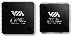
| VIA VT82C580VP Apollo VP-1 Chipset | ||
| Common Name | Apollo VP-1 | |
| Chipset Packaging | Number of chips | 3 (VT82C585VP, VT82C586, VT82C587VP) |
| Packaging Type | 2 x 208-pin QFP; 1 x 100-pin QFP | |
| CPU Support | Number of CPUs | 1 |
| AMD CPUs Supported | K5, K6 | |
| Cyrix CPUs Supported | 6x86 (M1), 6x86MX (M2) w/ Linear Burst Mode | |
| Intel CPUs Supported | Pentium, Pentium MMX | |
| Cache | Type | Asynchronous/Synchronous Pipeline Burst Cache |
| Maximum Supported Size | 2048KB | |
| Maximum Cacheable DRAM Area | 512MB | |
| Memory | Maximum DRAM Supported | 512MB |
| BEDO DRAM Read Timings (66MHz) | 5-1-1-1 | |
| EDO DRAM Read Timings (66MHz) | 5-2-2-2 | |
| FPM DRAM Read Timings (66MHz) | 5-3-3-3 | |
| SDRAM Read Timings (66MHz) | 5-1-1-1 | |
| Data Path to Memory | 64-bits | |
| ECC Support | No | |
| Hard Disk Controller | Chip | VIA BMIDE Controller (VT82C586) |
| Busmastering Support | Yes | |
| UltraDMA Support | Yes | |
| Max. Theoretical Transfer Rate | PIO Mode 5/DMA Mode 3 (33.3MB/S) | |
| PCI Interface | Supported PCI Bus Speeds | 25, 30, 33 MHz |
| Concurrent PCI | No | |
| Async. PCI Bus Speed | No | |
| PCI Specification | 2.0 (66 MHz max.) | |
| Power Management | PC97 Compliance | No |
| Suspend to Disk | No | |
| HDD Power Down | Yes | |
| Modem Wakeup | No | |
| System Suspend | No | |
| Video | AGP Support | No |
| Unified Memory Architecture | Yes | |
| Peripheral Support | USB Support | Yes |
| Plug and Play Port | Yes | |
| Write Buffers | CPU-to-DRAM | 16 QWords (?) |
| CPU-to-PCI | 6 DWords (?) | |
| PCI-to-DRAM | 48 DWords (?) | |
| Officially Supported Bus Speeds | 50, 60, 66 MHz | |
| Unofficially Achieved Bus Speeds | 75 MHz | |
 |
With the success VIA attained with the VP-1 and VPX chipsets it was time to drop a huge bomb on the competition by announcing a head to head competitor of Intel's latest and greatest TX chipset. VIA did just that with the announcement of the VP2/97 chipset, and it was that announcement that allowed them to gain the support of some of the industry's biggest names, including Advanced Micro Devices with the release of their AMD K6 Microprocessor. |
The VIA VP2/97 chipset combines the best features found in all Socket-7 chipsets, from BEDO and SDRAM support to UMA and UltraDMA support, the VP2/97 topples the competition with a rich feature set. The unique two chip solution from VIA packs a strong punch with, once again, a maximum of 512MB (all cached) RAM complimented by the large 2MB of L2 cache possible with the VP2/97. Supporting all processor classes from the early Pentium Classic to the Cyrix 6x86MX with support for Intel and Linear Burst Mode SRAM transfers the VP2/97 is truly a chipset for the masses.
Like Intel's TX chipset, the power saving features on the VP2/97 are tremendous which is a direct result of its PC97 compliance. The VP2/97 is in a class of its own since NO other Socket-7 chipset can even begin to support the features the VP2/97 boasts. The only downside to the VP2/97 is that it doesn't support AGP, which will be featured in the successor to the VP2/97, the VIA VP3 chipset.
| VIA VT82C590 Apollo VP2/97 Chipset | ||
| Common Name | Apollo VP2/97 | |
| Chipset Packaging | Number of chips | 2 (VT82C595 North Bridge, VT82C586B South Bridge) |
| Packaging Type | 1 x 328-pin BGA; 1 x 208-pin QFP | |
| CPU Support | Number of CPUs | 1 |
| AMD CPUs Supported | K5, K6 | |
| Cyrix CPUs Supported | 6x86 (M1), 6x86MX (M2) w/ Linear Burst Mode | |
| Intel CPUs Supported | Pentium, Pentium MMX | |
| Cache | Type | Synchronous Pipeline Burst Cache |
| Maximum Supported Size | 2048KB | |
| Maximum Cacheable DRAM Area | 512MB | |
| Memory | Maximum DRAM Supported | 512MB |
| BEDO DRAM Read Timings (66MHz) | 5-1-1-1 | |
| EDO DRAM Read Timings (66MHz) | 5-2-2-2 | |
| FPM DRAM Read Timings (66MHz) | 5-3-3-3 | |
| SDRAM Read Timings (66MHz) | 3-1-1-1 | |
| Data Path to Memory | 64-bits | |
| ECC Support | Yes | |
| Hard Disk Controller | Chip | VIA South Bridge Controller (VT82C586B) |
| Busmastering Support | Yes | |
| UltraDMA Support | Yes | |
| Max. Theoretical Transfer Rate | PIO Mode 5/DMA Mode 3 (33.3MB/S) | |
| PCI Interface | Supported PCI Bus Speeds | 25, 30, 33 MHz |
| Concurrent PCI | Yes | |
| Async. PCI Bus Speed | No | |
| PCI Specification | 2.0 (66 MHz max.) | |
| Power Management | PC97 Compliance | Yes |
| Suspend to Disk | Yes | |
| HDD Power Down | Yes | |
| Modem Wakeup | Yes | |
| System Suspend | Yes | |
| Video | AGP Support | No |
| Unified Memory Architecture | Yes | |
| Peripheral Support | USB Support | Yes |
| Plug and Play Port | Yes | |
| Write Buffers | CPU-to-DRAM | 16 QWords |
| CPU-to-PCI | 6 DWords | |
| PCI-to-DRAM | 48 DWords | |
| Officially Supported Bus Speeds | 50, 60, 66 MHz | |
| Unofficially Achieved Bus Speeds | 68, 75, 83.3 MHz | |
VIA is now the ultimate competitor to Intel's tyranny in the Chipset market, and although they aren't as large or as powerful as the microprocessor giant they produce chipsets that have toppled even Intel's best efforts in this industry.
 |
With the success of the original Apollo VP chipset, a supposed competitor of the Intel 430FX chipset although it blew it away in most instances, VIA decided to implement some next generation features into their hot topic VPX chipset. By raising the cacheable memory limit to 512MB, giving the user a maximum of 2MB of L2 cache, and allowing us to take advantage of such features as UltraDMA hard drives and SDRAM (features only found in Intel's TX and LX chipsets) VIA accomplished in producing a superior product in nearly every aspect to Intel's lackluster 430 series of chipsets. VIA embraced all CPU manufacturers with the release of the Apollo VPX by allowing support for normal Intel Burst Modes as well as the elusive Linear Burst Mode reserved for IBM/Cyrix processors. |
Unfortunately many motherboard manufacturers couldn't properly harness this power, and therefore quite a few users were disappointed with VPX based systems since they were poorly designed. However, a few companies were able to take advantage of the amazing capabilities of this chipset. Among these companies, FIC, seemed to be the most successful in achieving the maximum potential of the VPX chipset with their PA-2010+.
The VPX chipset features many of the useful options we all loved from the HX and VX chipsets, while adding some of its own unique characteristics such as BEDO DRAM support with a timing of 5-1-1-1. The VPX, like Intel's VX chipset supports UMA and SDRAM, however the VPX's SDRAM timings are much faster than those of Intel's VX chipset. If you combine the extensive memory support of the VPX chipset, as well as its support for UltraDMA/33 hard drives the VPX begins to look much less like a competitor and much more like a dominator in the chipset industry.
| The VPX chipset is also fully PC97 compliant, however a more affordable version without PC97 compliance is available for entry level systems consisting of the VT82C585VPX and VT82C586A instead of the VT82C585VPX north bridge and VT82C586B south bridge controllers. |  |
| VIA VT82C580VPX Apollo VPX/97 Chipset | ||
| Common Name | Apollo VPX/97 | |
| Chipset Packaging | Number of chips | 2 (VT82C595 North Bridge Controller, VT82C586B South Bridge) |
| Packaging Type | 2 x 208-pin QFP | |
| CPU Support | Number of CPUs | 1 |
| AMD CPUs Supported | K5, K6 | |
| Cyrix CPUs Supported | 6x86 (M1), 6x86MX (M2) w/ Linear Burst Mode | |
| Intel CPUs Supported | Pentium, Pentium MMX | |
| Cache | Type | Asynchronous/Synchronous Pipeline Burst Cache |
| Maximum Supported Size | 2048KB | |
| Maximum Cacheable DRAM Area | 512MB | |
| Memory | Maximum DRAM Supported | 512MB |
| BEDO DRAM Read Timings (66MHz) | 5-1-1-1 | |
| EDO DRAM Read Timings (66MHz) | 5-2-2-2 | |
| FPM DRAM Read Timings (66MHz) | 5-3-3-3 | |
| SDRAM Read Timings (66MHz) | 3-1-1-1 | |
| Data Path to Memory | 64-bits | |
| ECC Support | No | |
| Hard Disk Controller | Chip | VIA South Bridge Controller (VT82C586B) |
| Busmastering Support | Yes | |
| UltraDMA Support | Yes | |
| Max. Theoretical Transfer Rate | PIO Mode 5/DMA Mode 3 (33.3MB/S) | |
| PCI Interface | Supported PCI Bus Speeds | 25, 30, 33 MHz |
| Concurrent PCI | Yes | |
| Async. PCI Bus Speed | Yes | |
| PCI Specification | 2.0 (66 MHz max.) | |
| Power Management | PC97 Compliance | Yes |
| Suspend to Disk | Yes | |
| HDD Power Down | Yes | |
| Modem Wakeup | Yes | |
| System Suspend | Yes | |
| Video | AGP Support | No |
| Unified Memory Architecture | Yes | |
| Peripheral Support | USB Support | Yes |
| Plug and Play Port | Yes | |
| Write Buffers | CPU-to-DRAM | 16 QWords |
| CPU-to-PCI | 6 DWords | |
| PCI-to-DRAM | 48 DWords | |
| Officially Supported Bus Speeds | 50, 60, 66, 75 MHz | |
| Unofficially Achieved Bus Speeds | 68, 83.3 MHz | |
Hoping to destroy the competition Intel announced and released their 440LX chipset late in 1997 with support for AGP, however that AGP support is limited to the Slot-1 Architecture of the Pentium II since Intel announced that they would not produce an AGP equipped Pentium Chipset. This produced a tremendous opportunity for some of the other chipset manufacturers to step up and satisfy the market. VIA, being the leading contender for Intel's throne, decided to use this to their advantage. The result of their efforts? The VIA Apollo VP3 Chipset, the first AGP capable Pentium Chipset.
Take all of the features of the VP2/97 chipset, double the CPU-to-DRAM Write Buffers, add a full gigabyte of cacheable memory area (which is greater than the 512MB supported by the Pentium II!!!) and AGP support and you get the Apollo VP3 chipset. As the VP2/97 was essentially a combination of the Intel HX and TX chipsets, the VP3 is a combination of the VIA VP2 and the Intel 440LX chipsets. Although the performance of the VP3 has yet to be proven, it will soon by FIC with the release of their PA-2012, the very first Socket-7 AGP Motherboard. VIA has a huge hit on their hands with the combination of the success of the VP2/97 and the imminent success of the VP3 chipset.
Unfortunately there are two significant "let downs" the VP3 chipset leaves us with. The first isn't all that prominent, just that the VP3 doesn't support BEDO DRAM like its predecessors the VP2 and VPX did. Its support for SDRAM as well as DDR-SDRAM does compensate for that shortcoming so it really isn't a huge problem for most users. The big letdown is the lack of a 100MHz bus speed support natively with the VP3 chipset, we will unfortunately have to wait for the next stop in VIA's travels for 100MHz bus speed support with the MVP3 (Mobile VP3).
| VIA VT82C Apollo VP3 Chipset | ||
| Common Name | Apollo VP3 | |
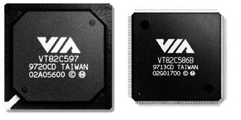
| Chipset Packaging | Number of chips | 2 (VT82C597 System Controller, VT82C586B PCI-to-ISA Bridge) |
| Packaging Type | 1 x 472-pin BGA; 1 x 208-pin QFP | |
| CPU Support | Number of CPUs | 1 |
| AMD CPUs Supported | K5, K6 | |
| Cyrix CPUs Supported | 6x86 (M1), 6x86MX (M2) w/ Linear Burst Mode | |
| Intel CPUs Supported | Pentium, Pentium MMX | |
| Cache | Type | Synchronous Pipeline Burst Cache |
| Maximum Supported Size | 2048KB | |
| Maximum Cacheable DRAM Area | 1GB | |
| Memory | Maximum DRAM Supported | 1GB |
| BEDO DRAM Read Timings (66MHz) | N/A | |
| EDO DRAM Read Timings (66MHz) | 5-2-2-2 | |
| FPM DRAM Read Timings (66MHz) | 5-3-3-3 | |
| SDRAM Read Timings (66MHz) | 3-1-1-1 | |
| Data Path to Memory | 64-bits | |
| ECC Support | Yes | |
| Hard Disk Controller | Chip | VIA BMIDE Controller (VT82C586B) |
| Busmastering Support | Yes | |
| UltraDMA Support | Yes | |
| Max. Theoretical Transfer Rate | PIO Mode 5/DMA Mode 3 (33.3MB/S) | |
| PCI Interface | Supported PCI Bus Speeds | 25, 30, 33 MHz |
| Concurrent PCI | Yes | |
| Async. PCI Bus Speed | No | |
| PCI Specification | 2.0 (66 MHz max.) | |
| Power Management | PC97 Compliance | Yes |
| Suspend to Disk | Yes | |
| HDD Power Down | Yes | |
| Modem Wakeup | Yes | |
| System Suspend | Yes | |
| Video | AGP Support | Yes |
| Unified Memory Architecture | No | |
| Peripheral Support | USB Support | Yes |
| Plug and Play Port | Yes | |
| Write Buffers | CPU-to-DRAM | 32 QWords |
| CPU-to-PCI | 6 DWords | |
| PCI-to-DRAM | 48 DWords | |
| Officially Supported Bus Speeds | 50, 60, 66 MHz | |
| Unofficially Achieved Bus Speeds | Unknown | |

With ALi boasting support for the 100MHz Frontside Bus and a large cacheable memory area, how could VIA resist but to release a Super7 candidate of their own? Originally, the VIA VP3 was expected to be the very first 100MHz + Socket-7 + AGP motherboard, unfortunately VIA dropped a bombshell on the market by announcing that the VP3 wouldn't support any bus speeds greater than 66MHz. At the same time VIA hinted at a Mobile-VP3 chipset, the MVP3, that would actually support the 100MHz bus speed & AGP. Now, under a year later, the MVP3 chipset is almost ready to make its grand-entrance, how grand will it be? We can only speculate.
In spite of the name, the Mobile VP3 can be used in both Desktop and Mobile motherboard solutions, this versatility will prove to be beneficial for VIA since no other chipset manufacturer has a chipset that will officially run the 100MHz on a Notebook system. In the desktop arena, the MVP3 will definitely be a competitor to the Aladdin V by ALi, with both chipsets supporting all of the features the Intel TX chipset does adding support for a 100MHz Frontside bus, as well as AGP 2x support. The MVP3 differs from the Aladdin V in two major areas, both involving RAM...let's explore the two differences.
While the Aladdin V only supports EDO, FPM, and SDRAM, the MVP3 supports JEDEC BDDR SDRAM-II (Bi Directional Double Data Rate SDRAM), Virtual Channel SDRAM, and Enhanced SDRAM. While those last few SDRAM types are next to impossible to come across that may change if the demand for SDRAM-II modules increases, possibly by the success of a chipset that supports the standard. Its a heavy weight to put on the MVP3's unreleased shoulders, but it is there nevertheless.
Speaking of RAM, the MVP3 chipset introduces a unique feature into the Super7 arena, the ability to run the Memory Bus Speed at 66MHz, while using a 100MHz Bus Speed to derive the Processor Clock. This means that, in theory, you could even re-use your old generic 60ns EDO SIMMs on a MVP3 motherboard. Not a bad feature for VIA to include.
The only other real difference between the MVP3 and the Aladdin V is that the MVP3 doesn't feature any Internal L2 cache bits/Tag RAM bits, making high quality L2 cache with a fast Tag RAM chip a necessity for all MVP3 boards if you plan on using them with the 100MHz bus speed. This introduces a new factor into achieving system stability, L2 cache quality, if a manufacturer of a MVP3 motherboard decides to skimp on the L2 cache and include 8 or even 10ns SRAM chips, expect to have problems galore at 100MHz.
An interesting note, unlike all previous VIA Socket-7 chipsets, the MVP3 only features an integrated 8-bit Tag comparator while the VP2 for example features an integrated 10-bit Tag comparator. Translation? Don't expect MVP3 motherboards to be able to cache the supported 1GB of RAM, in combination with the L2 cache sizes and Tag RAM chips that will be used on most MVP3 motherboards, expect cacheable memory areas to range from 256MB down to 64MB. While waiting for an official word from VIA on this issue, it seems highly unlikely that MVP3 motherboards will be able to compete with Aladdin V boards in terms of cacheable memory areas.
Performance wise, in spite of the fewer CPU-to-DRAM write buffers, the MVP3 should be on the heels of the Aladdin V, outperforming the Intel TX chipset at the 66MHz bus speed and leaving it behind when clocked at 100MHz.
VIA has been in the lime light of the chipset industry for much longer than Acer Labs has, so it'll take quite a bit for VIA to throw in the towel in the Super7 battle. Expect the MVP3 to be the Aladdin V's biggest competitor, in the end it will most likely come down to a battle among motherboard manufacturers to completely harness the immense power of one of these two chipsets.
| VIA VT82C Apollo Mobile VP3 Chipset | ||
| Common Name | Apollo MVP3 | |
| Chipset Packaging | Number of chips | 2 (VT82C598AT System Controller, VT82C586B PCI-to-ISA Bridge) |
| Packaging Type | 1 x 476-pin BGA; 1 x 208-pin QFP | |
| CPU Support | Number of CPUs | 1 |
| AMD CPUs Supported | K5, K6, K6-3D | |
| Cyrix CPUs Supported | 6x86 (M1), 6x86MX (M2) w/ Linear Burst Mode Support | |
| Intel CPUs Supported | Pentium, Pentium MMX | |
| Cache | Type | Synchronous Pipeline Burst Cache |
| Maximum Supported Size | 2048KB | |
| Maximum Cacheable DRAM Area | ??? | |
| Memory | Maximum DRAM Supported | 1GB |
| BEDO DRAM Read Timings (66MHz) | N/A | |
| EDO DRAM Read Timings (66MHz) | 5-2-2-2 | |
| FPM DRAM Read Timings (66MHz) | 5-3-3-3 | |
| SDRAM Read Timings (66MHz) | 3-1-1-1 | |
| Data Path to Memory | 64-bits | |
| ECC Support | Yes | |
| Hard Disk Controller | Chip | VIA BMIDE Controller (VT82C586B) |
| Busmastering Support | Yes | |
| UltraDMA Support | Yes | |
| Max. Theoretical Transfer Rate | PIO Mode 5/DMA Mode 3 (33.3MB/S) | |
| PCI Interface | Supported PCI Bus Speeds | 25, 30, 33 MHz |
| Concurrent PCI | Yes | |
| Async. PCI Bus Speed | Yes (Pseudo Synchronous) | |
| PCI Specification | 2.1 (66 MHz max.) | |
| Power Management | PC97 Compliance | Yes |
| Suspend to Disk | Yes | |
| HDD Power Down | Yes | |
| Modem Wakeup | Yes | |
| System Suspend | Yes | |
| Video | AGP Support | Yes |
| Unified Memory Architecture | No | |
| Peripheral Support | USB Support | Yes |
| Plug and Play Port | Yes | |
| Write Buffers | CPU-to-DRAM | 16 QWords |
| CPU-to-PCI | 5 DWords | |
| PCI-to-DRAM | 48 DWords | |
| Officially Supported Bus Speeds | 50, 60, 66, 75, 83, 100 MHz | |
| Unofficially Achieved Bus Speeds | Unknown | |
While Intel accepted the fact that they had the sole production of Slot-1 chipset solutions in their hands, VIA was working hard, both on the legal and engineering ends of things, to produce the perfect Slot-1 compatible chipset they could possibly produce, the results? The VIA Apollo Pro chipset.
Supporting all of the features of the Intel 440BX AGPSet, the Apollo Pro is much more than an alternative to the BX Chipset as it brings much more than AGP and SDRAM support to the game. Support for 5 PCI master devices (compared to the 3 PCI masters on Intel chipsets) make the Apollo Pro ideal for an ISA Slot-less motherboard, in theory, with the use of an additional PCI-to-PCI bridge, a motherboard featuring 7 PCI slots could be constructed although only 6 of them would be usable at one time as long as a card populated the AGP slot. Expect to see a minimum of 5 PCI slots on most Apollo Pro based motherboard solutions. In addition to that, the Apollo Pro, like the VIA MVP3, does support the operation of the memory bus at an external frequency identical to that of the AGP Clock. Meaning you can run your memory banks at the 66MHz Front Side Bus, while your processor's speed is derived from the 100MHz FSB. This will allow you to re-use your old PC66 DIMMs and even your old EDO/FP DIMMs so long as they work at the 66MHz FSB.
The Apollo Pro's supported DRAM types extends far beyond the normal EDO/FP/SDRAM list, to include DDR (Double Data Rate) SDRAM. While this looks wonderful on paper, the absence of DDR SDRAM in the mainstream market will keep that feature from becoming a reason to opt for an Apollo Pro based board over an Intel chipset based model. Expect performance of Apollo Pro based Pentium II boards to be at least on par with that of well designed BX motherboards, with the first boards shipping in the next month or two we should soon be able to find out if the Apollo Pro is everything it is cracked up to be.
A downside to the Apollo Pro is that, unlike the Intel LX/BX/GX series, you must use VIA's own AGP GART drivers to get the full benefit of the supported AGP port which may introduce some issues with future video cards and chipsets, nothing that a simple driver patch won't fix but something to keep in mind.
| VIA Apollo Pro Chipset | ||
| Common Name | VIA Apollo Pro Chipset | |
| Chipset Packaging | Number of chips | 1 (VT82C691 North Bridge) |
| Packaging Type | 1 x 492-pin BGA | |
| CPU Support | Number of CPUs | 1 |
| AMD CPUs Supported | N/A | |
| Cyrix CPUs Supported | N/A | |
| Intel CPUs Supported | Pentium II, Pentium Pro | |
| Cache | Type | N/A on chip |
| Maximum Supported Size | N/A on chip | |
| Maximum Cacheable DRAM Area | N/A on chip | |
| Memory | Maximum DRAM Supported | 1GB |
| BEDO DRAM Read Timings (100MHz) | N/A | |
| EDO DRAM Read Timings (100MHz) | X-2-2-2 | |
| FPM DRAM Read Timings (100MHz) | X-4-4-4 | |
| SDRAM Read Timings (100MHz) | X-1-1-1 | |
| Data Path to Memory | 64-bits | |
| ECC Support | Yes | |
| Hard Disk Controller | Chip | VT82C596 South Bridge |
| Bus Mastering Support | Yes | |
| UltraDMA Support | Yes | |
| Max. Theoretical Transfer Rate | PIO Mode 5/DMA Mode 3 (33.3MB/S) | |
| PCI Interface | Supported PCI Bus Speeds | 30, 33 MHz |
| Async. PCI Bus Speed | No | |
| PCI Specification | 2.1 (66 MHz max.) | |
| Power Management | PC97 Compliance | Yes |
| Suspend to Disk | Yes | |
| HDD Power Down | Yes | |
| Modem Wakeup | Yes | |
| System Suspend | Yes | |
| Video | AGP Support | Yes (66/133) |
| Unified Memory Architecture | No | |
| Peripheral Support | USB Support | Yes |
| Plug and Play Port | Yes | |
| Officially Supported Bus Speeds | 66, 100 MHz | |
| Unofficially Achieved Bus Speeds | 112, 124MHz | |
Here is an odd chipset you might've heard of in your experiences with motherboards and chipsets, the elusive VXPro chipset, found mostly in PCChips motherboards. Although it is often referred to as a cheap imitation of the Intel 430VX chipset, the VXPro does have its advantages over Intel's design, mainly dealing with cost.
The VXPro+ Chipset fully supports UltraDMA hard drives and SDRAM, unfortunately it doesn't feature the fast SDRAM timings found in the Intel TX and VIA Apollo VP2 chipsets which degrade its quality as a whole. However, the VXPro was never intended to be marketed under any labels, although the technology was apparently licensed to PCChips for use in their motherboards by VIA. VXPro chipset would appear to be loosely based on the VIA Apollo VP-1, however it seems to be a much cheaper version of it directed at entry level users. The VXPro was intended to be more of a head to head competitor of Intel's VX chipset, including features such as UMA support.
As far as most information sources goes, the VXPro chipset still limits the cacheable memory area to 64MB and unfortunately it doesn't support the maximum 2MB of L2 cache found in the superior Apollo VP-1. The VXPro chipset does however support the use of Concurrent PCI/CPU operations as well as an asynchronous PCI bus (i.e. the PCI bus can be set to 33MHz regardless of the external bus speed). The only area in which the VXPro really excels however, aside from the fact that the VXPro+ supports the UltraATA extension, is its amazing price. A motherboard built around the VXPro chipset will most likely go for about $60 which isn't bad for someone looking for an affordable solution for a second or third computer, possibly even a low cost business workstation.
| VIA VXPro/VXPro+ Chipset | ||
| Common Name | VXPro | |
| Chipset Packaging | Number of chips | 2 (VT82C585, VT82C586) |
| Packaging Type | 2 x 208-pin QFP | |
| CPU Support | Number of CPUs | 1 |
| AMD CPUs Supported | K5, K6 | |
| Cyrix CPUs Supported | 6x86 (M1), 6x86MX (M2) | |
| Intel CPUs Supported | Pentium, Pentium MMX | |
| Cache | Type | Asynchronous/Synchronous Pipeline Burst Cache |
| Maximum Supported Size | 512KB | |
| Maximum Cacheable DRAM Area | 64MB | |
| Memory | Maximum DRAM Supported | 128MB |
| BEDO DRAM Read Timings (66MHz) | N/A | |
| EDO DRAM Read Timings (66MHz) | 5-2-2-2 | |
| FPM DRAM Read Timings (66MHz) | 5-3-3-3 | |
| SDRAM Read Timings (66MHz) | 7-1-1-1 | |
| Data Path to Memory | 64-bits | |
| ECC Support | No | |
| Hard Disk Controller | Chip | VIA BMIDE Controller (VT82C586) |
| Busmastering Support | Yes | |
| UltraDMA Support | Yes | |
| Max. Theoretical Transfer Rate | PIO Mode 5/DMA Mode 3 (33.3MB/S) | |
| PCI Interface | Supported PCI Bus Speeds | 25, 30, 33 MHz |
| Concurrent PCI | Yes | |
| Async. PCI Bus Speed | Yes | |
| PCI Specification | 2.0 (66 MHz max.) | |
| Power Management | PC97 Compliance | No |
| Suspend to Disk | No | |
| HDD Power Down | Yes | |
| Modem Wakeup | No | |
| System Suspend | No | |
| Video | AGP Support | No |
| Unified Memory Architecture | Yes | |
| Peripheral Support | USB Support | Yes |
| Plug and Play Port | Yes | |
| Write Buffers | CPU-to-DRAM | Unknown |
| CPU-to-PCI | Unknown | |
| PCI-to-DRAM | Unknown | |
| Officially Supported Bus Speeds | 50, 60, 66 MHz | |
| Unofficially Achieved Bus Speeds | 75, 83 MHz | |


