Original Link: https://www.anandtech.com/show/828
NVIDIA's nForce 420/220: It's finally here
by Anand Lal Shimpi on September 24, 2001 8:26 AM EST- Posted in
- CPUs
It's been three months, two weeks and six days since we introduced you to NVIDIA's nForce chipset. The chipset literally stole the show at this year's Computex. By the end of our stay in Taiwan our number one question to the motherboard manufacturers we visited was "what are your thoughts on nForce?" NVIDIA quite honestly had VIA very worried at Computex. The original launch schedule placed nForce review samples in the hands of editors towards the end of June; months before VIA could have their KT266A ready. After already receiving a heavy blow from SiS with the barrage of SiS 735 chipset reviews prior to Computex, VIA was in no shape to deal with an even more formidable opponent.
Luckily for VIA, this is NVIDIA's first shot at making a PC chipset. As many of you are probably wondering, what exactly took the nForce this long to end up in a final production ready state? NVIDIA overestimated themselves; based on their experiences in the add-in graphics card industry they assumed a successful chipset rollout would be very similar to what they had encountered in the past. As we heard from virtually every single one of the motherboard manufacturers that NVIDIA had given samples to, nForce was hardly ready for prime time at Computex.
We actually managed to spend some time benchmarking the various nForce motherboards ready for Computex. The motherboards were plagued with stability problems and were not performing up to par. This was in fact the biggest complaint motherboard manufacturers had with initial revs of the nForce chipset; the performance was not up to par with what NVIDIA was claiming. A very painful and rigorous revision process ensued over the coming months with a new chipset revision or BIOS revision coming almost every week. These weren't minor revisions either; from what the motherboard manufacturers had told us, they were apparently pretty serious hardware revisions occurring many times over the course of a single month.
NVIDIA was learning though; when they first approached their five launch partners and wanted a performance debut of the chipset at or shortly after Computex it was clear that they were newcomers to this sector. But it didn't take more than a couple of months later for things to turn around. Worries of whether the chipset would even hit the streets this year were finally put to rest, and the chipset was quickly nearing a production level state. NVIDIA was also improving their understanding of the lead times the motherboard manufacturers needed to produce a solid board design. Today we're finally able to let you all know that the nForce is ready and very capable of being benchmarked, which is exactly what we did.
We've actually been playing around with the nForce for over a month now and its performance was there weeks ago, but the stability of NVIDIA's reference board design was only just recently solidified. With a final product in hand and production quality drivers, we set out to review the most versatile desktop chipset to ever hit the market.
nForce: The Architecture
In spite of the rumors that were spread, the final nForce chipset is no different than what we reported on in our original article. The chipset is very unique because it is a clear departure from the conventional role a chipset plays in today's PC. While we won't go into too much depth here since we have covered its architecture in great detail already, it is worth noting that there are a few key points to keep in mind when looking at the nForce.
The chipset is split into two parts, as are most of today's chipsets; the Integrated Graphics Processor (IGP) and the Media & Communications Processor (MCP). With the release of the GeForce 256 "GPU", NVIDIA has been on a roll with calling everything possible a "processor" but in the case of the nForce they have very good reason to.
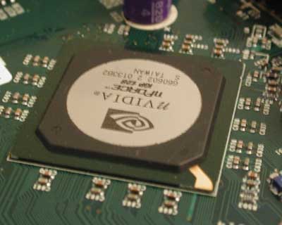
The IGP assumes the role of the conventional North Bridge or Memory Controller Hub (MCH - Intel chipsets) in a chipset. This role is generally to house an interface to the processor, AGP graphics, memory and an interface to the South Bridge or I/O Controller Hub (ICH – Intel chipsets). NVIDIA took the role of the North Bridge one step further with the IGP:
TwinBank Memory Architecture
The IGP-128 features two independent 64-bit SDR/DDR SDRAM memory controllers. In contrast, all other chipsets with DDR SDRAM support only have a single 64-bit DDR SDRAM memory controller. The benefit of having two 64-bit controllers is that you get twice as much memory bandwidth; the only constraint being that you must use two 64-bit DIMMs in order to achieve the 128-bit width which makes sense. In the case of the current nForce, the added bandwidth of going to a dual channel (via two controllers) DDR SDRAM memory bus is not really used. The reason being that the Athlon's FSB can only provide bandwidth equivalent to one 64-bit DDR266 SDRAM channel (2.1GB/s) not two (4.2GB/s). This makes the IGP-64, with only a single 64-bit SDR/DDR SDRAM controller, much more sensible for most users.
Integrated GeForce2 MX Graphics
Both versions of the IGP (IGP-128 and IGP-64) feature an integrated GeForce2 MX core running at 175MHz. This is what gives the IGP its name and it's also what makes the added bandwidth of the TwinBank Memory Architecture useful. The biggest performance constraint when dealing with integrated video solutions is memory bandwidth; there's simply not enough. Although the GeForce2 MX graphics core shares the same memory bandwidth as the rest of the system in the case of the nForce, there is enough spare memory bandwidth to offer performance very close to that of a regular GeForce2 MX. Remember that a regular GeForce2 MX has 2.7GB/s of memory bandwidth through a 128-bit SDRAM interface running at 166MHz. While the integrated GeForce2 MX on the nForce can theoretically have up to 4.2GB/s of bandwidth dedicated to itself but we all know that the CPU and peripherals will eat into that bandwidth. Realistically, at least half of that bandwidth should be available for the integrated core to use.
The amount of system memory that will be used for the GPU's frame buffer is selectable from within the BIOS. NVIDIA's reference board only allows a maximum of 32MB to be allocated at this point but even they will admit that 64MB is overkill for today's games.
The IGP also has an internal AGP bus that can be clocked at 100MHz (instead of the 66MHz clock for normal AGP buses) for transfer rates equivalent to an AGP 6X mode. While the integrated GPU will rely on the TwinBank memory controllers to provide a path to its shared frame buffer, as soon as that frame buffer is exceeded or data is requested to be transferred over the AGP bus the data will flow over this internal 100MHz AGP bus. No games today are triangle setup intensive enough to actually see a gain in performance with this 100MHz internal AGP bus, but future versions of the nForce chipset could prove the feature to be useful when more triangle data is sent between the CPU and GPU over the AGP bus.
Of course you're not constrained to use the integrated GPU and NVIDIA has included an external AGP 4X interface (operating at 66MHz) with the IGP for just this purpose. Any AGP card will work in the nForce's external AGP slot so long as it is keyed for 1.5V operation. The only recently cards not keyed for 1.5V operation are the former 3dfx Voodoo4 and Voodoo5 cards which won't physically fit in the AGP slot.
Dynamic Adaptive Speculative Pre-Processor (DASP)
Much like Intel's 845 chipset, nForce features an intelligent 8-way set associative prefetch cache in the IGP to reduce latency by looking at data access patterns and prefetching data into this cache before the CPU or GPU needs it. If the data ends up being useful, it is already cached and thus much quicker to retrieve; if it isn't useful it is just as easily discarded with no harm done.
nForce Media & Communications Processor
The power doesn't stop at the IGP; the Media & Communications Processor (MCP) of the nForce is also a very powerful part of the package. The conventional role played by the South Bridge is to provide legacy connectivity to older buses, to provide PCI, IDE and USB interfaces, and sometimes integrated Ethernet/audio controllers. The nForce MCP takes that one step further by including the most powerful integrated audio processor available to date.
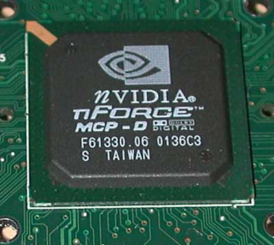
The MCP is outfitted with what NVIDIA calls their Audio Processing Unit (APU), a licensed implementation of Parthus' MediaStream DSP. In order to deal with licensing issues a separate version of the MCP named MCP-D is produced with support for real time Dolby Digital Encoding. In reality, there is no difference between the hardware of the MCP and the MCP-D it's just that in the latter case, Dolby Digital Encoding is enabled.
The MCP is connected to the IGP through the very first publicly available implementation of AMD's HyperTransport technology. For more information about the MCP, HyperTransport and the rest of the nForce architecture take a look at our nForce Preview.
nForce: The Reference Board
In our original article we described the two major incarnations of the nForce chipset, the nForce 220 and the nForce 420. The only difference between the two is the presence (or lack thereof) the TwinBank memory controllers; the nForce 420 uses the 128-bit TwinBank memory controllers and thus has the IGP-128 while the nForce 220 has the 64-bit IGP-64. Another designation is made among chipsets based on the presence of the Dolby Digital license for the MCP. Appending a "-D" to the end of the chipset name indicates that a MCP-D is present while no trailing D indicates that Dolby Digital Encoding will not be available.

NVIDIA's reference board is a very well constructed implementation of the nForce 420-D chipset. The 4-layer microATX motherboard is intended to show off how cheap nForce motherboards can be made because of their 4-layer construction and ability to maintain fully functionality while being confined to a microATX form factor. The board features two PCI slots, 1 AGP slot and 1 ACR slot (the backwards PCI slot on the board).
Since the reference board does use the 420 chipset, there are two independent memory banks present. The first is a single 184-pin DDR SDRAM bank and the second is a combination of two 184-pin DDR SDRAM banks. In order for you to take advantage of the two memory controllers a DIMM must be present in the single bank and one DIMM must be present in one of the two remaining slots. Otherwise the motherboard will default to 64-bit operation, effectively making this board a 220-D.
There are a few notable shortcomings about the reference board. First of all, there is no Ethernet physical layer on the motherboard itself and thus no Ethernet header. The Ethernet controller was enabled in the MCP-D and drivers could be installed but there was no way to test the Ethernet performance due to the lack of an Ethernet header. Fortunately, most motherboard manufacturers seem to be outfitting their nForce boards with an Ethernet header.
The other problem is that in spite of the "-D" designation on the MCP, the motherboard features no digital output connector. The only audio ports are the conventional speaker out and the line/mic inputs. According to NVIDIA, a separate ACR card is necessary to gain the digital output necessary for outputting a Dolby Digital encoded signal. We sincerely hope that when the big-five manufacturers come forth with their nForce solutions that they make it a point to either include the appropriate ACR card or some other means of having a digital output connector otherwise one of the biggest features of the chipset will have gone to waste.
Because of these two issues with the reference design, we were not able to test the Ethernet performance of the solution nor its ability to achieve real time Dolby Digital encoding. We did test the basic audio functionality however.
One Driver Fits All
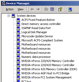
A very attractive point of the nForce platform is that a single manufacturer will be able to provide you with driver updates for virtually every part of your system (audio, video, Ethernet, chipset). The nForce drivers we tested with were approximately 4MB zipped and contained the drivers for every part of the nForce motherboard (including Ethernet and Audio) except for the integrated GPU. For that we used NVIDIA's recently released Detonator XP drivers which detected the integrated GPU perfectly.
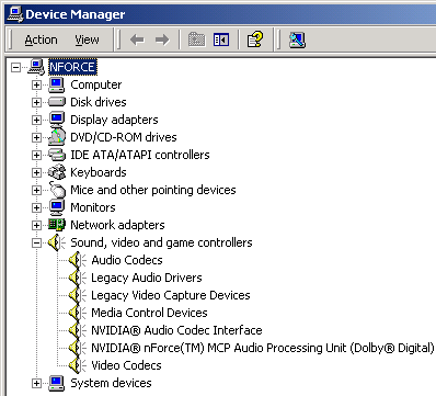
It's unusual seeing NVIDIA anywhere other than under Display Adapters
We had no compatibility issues with the drivers and versions will be available for 9x, Me, NT/2000 and XP.
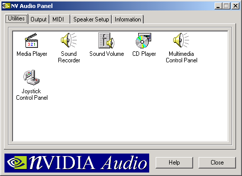
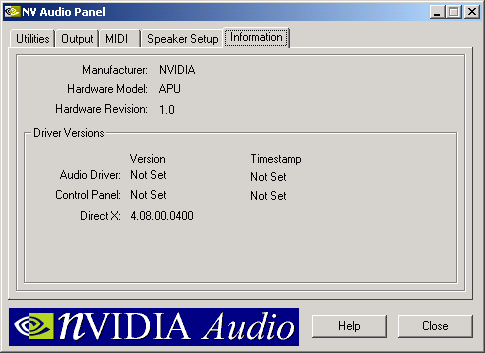
The drivers installed this NVIDIA control panel to adjust some of the features of the APU.
Testing the Beast
It's obvious that we couldn't have tackled this review like any other chipset review since there are too many variables we'd end up ignoring. Because of this we have divided the performance results into three distinct sections:
- Chipset comparison benchmarks comparing the nForce to the rest of the Socket-A chipset solutions
- Head to Head gaming performance tests comparing the nForce to its chief competitor: VIA's KT266.
- Audio performance vs. a SB Live!
In the future we hope to be able to better test the Ethernet and Dolby Digital capabilities of the MCP but as we mentioned earlier, the reference board would not allow it.
|
Windows 2000 Test System |
||||||
|
Hardware |
||||||
|
CPU(s) |
AMD Athlon-C 1.4GHz | |||||
| Motherboard(s) | ASUS
A7M266 (AMD760) ASUS A7V133 (KT133A) ECS K7S5A (SiS735) MSI K7T266 Pro (KT266) NVIDIA nForce 420-D Reference Board (nForce) VIA KT266A Reference Board (KT266A) |
|||||
| Memory |
256MB
DDR266 Crucial DDR SDRAM (Micron CAS2) |
|||||
| Hard Drive |
IBM Deskstar 30GB 75GXP 7200 RPM Ultra ATA/100 |
|||||
| CDROM |
Phillips 48X |
|||||
| Video Card(s) |
NVIDIA GeForce3 64MB DDR |
|||||
| Ethernet |
Linksys LNE100TX 100Mbit PCI Ethernet Adapter |
|||||
|
Software |
||||||
|
Operating System |
Windows 2000 Professional Service Pack 2 |
|||||
| Video Drivers |
|
|||||
Memory Bandwidth Performance
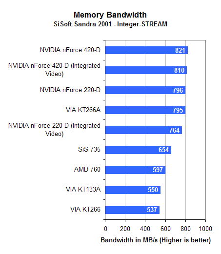
There are a couple of things to take away from this initial performance measurement. According to Sandra, the nForce 420-D only offers 26MB/s more useable memory bandwidth than the VIA KT266A. This is in spite of the fact that the 420-D has twice the theoretical memory bandwidth of the KT266A. The explanation is obvious and not too shocking; the Athlon is limited by its FSB in that the IGP can only get 2.1GB/s of data to it at any given time so having 4.2GB/s of memory bandwidth isn't all that useful. This is also an indicator that the nForce 220 should perform very similar to the 420.
The next point to take away from this is that by enabling the integrated video, in normal 2D usage there is only a 10 – 30MB/s memory bandwidth penalty. This is not significant enough to make a difference in any of the office/content creation benchmarks and sure enough it didn't.
The standings were virtually duplicated in the FP-STREAM results so we have omitted them since they didn't really add much to the review.
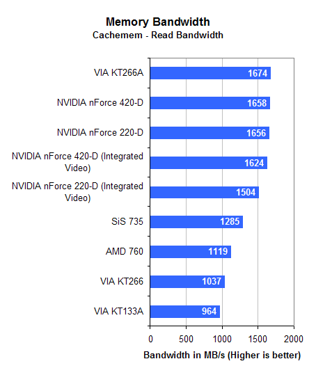
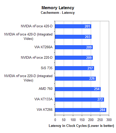
Cachemem is a bit more on the theoretical side when it comes to performance and as you can see here, the peak memory bandwidth of both nForce solutions is just a tad less than what the KT266A can offer. You can look at this one of two ways; either VIA designed an incredible memory controller with the KT266A or NVIDIA's solution is very well done for their first try.
Again we see that switching from an external AGP card to the nForce's integrated GPU results in a reduction of memory bandwidth which is to be expected. Here you can see that on the theoretical level, the reduction in bandwidth is much greater than what we saw in the more "real world" Sandra test. Keep in mind that neither of these benchmarks are very real world in that the performance differences here don't translate into real world performance figures; it's just useful to look at.
Memory Bandwidth Performance (continued)
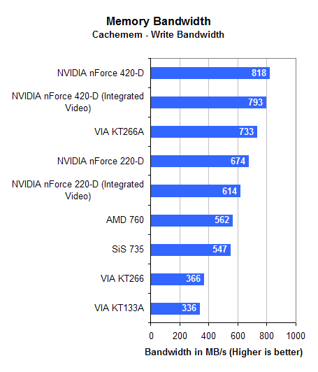
The nForce 420-D's write bandwidth is very impressive but what is quite interesting is the fact that it's noticeably higher than the 220-D's write bandwidth according to Cachemem. Shortly we'll be able to see exactly how much of this will translate into a real world performance difference between the two…
Here we see the positive effects of DASP and what happens when the IGP's arbiter has to deal with memory requests from the integrated GPU in addition to the CPU's requests. The only underpar performer here is the nForce 220-D with integrated video enabled where its latency is approaching that of the year old AMD 760 chipset.
Business & Content Creation Performance
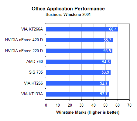
The KT266A continues to hold its high ground in the Business Winstone 2001 test, outpacing both the nForce solutions. Because of the disk intensive nature of this benchmark we can only hypothesize that VIA has tweaked their latest IDE drivers a bit more in the past few weeks to ensure such solid performance here.
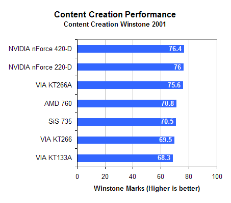
The same can't be said under Content Creation Winstone 2001 as the performance line between the KT266A and the nForce solutions grows blurry. All three of those chipsets perform within 1% of each other which is within the margin of error for this benchmark.
Also take note of the lack of performance difference between the nForce 420 and 220.
Business & Content Creation Performance (continued)
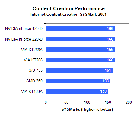
We've got another multi-way tie on our hands here. You can't really tell any performance difference between the SiS 735 and the nForce 420-D. It looks like we're getting very close to the peak performance of a DDR Athlon platform.
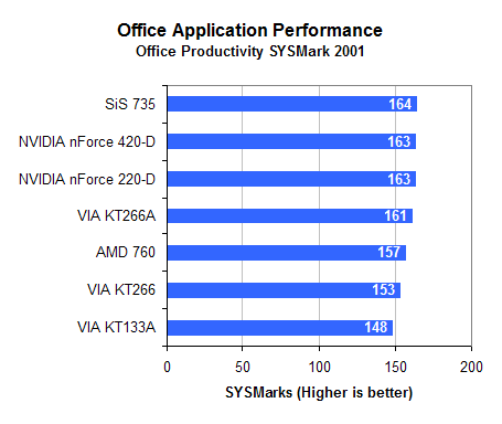
The picture doesn't change much as we look at office performance; the top four contenders are still within 1% of each other.
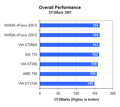
Two wrongs don't make a right and two ties don't mean exciting SYSMark results. It's clear from these first few benchmarks that the performance of the nForce is on-par with that of the KT266A. The real question, how much more impressive would these numbers have been had they been presented shortly after Computex in June?
3D Rendering & Animation Performance
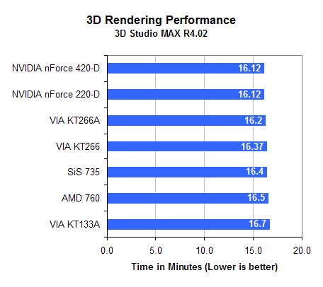
We know from previous investigations that there are some tests that simply aren't memory bandwidth intensive enough to show any difference between these similar platforms; 3D Studio MAX is one of them.
Once again we see that the performance of the two nForce solutions is on par with that of the KT266A.
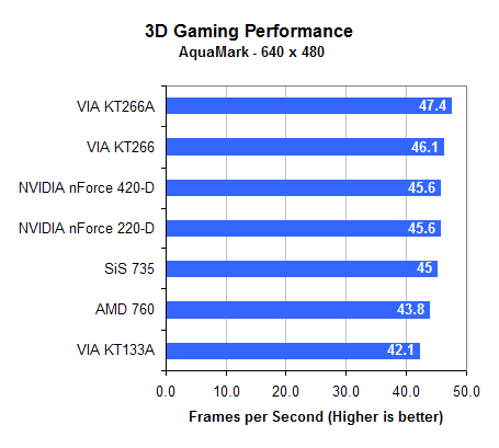
Gaming Performance
If memory bandwidth bottlenecks were not limitations on today's video cards, here's the kind of performance these chipsets would be able to contribute to our overall gaming experience:
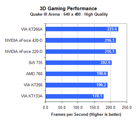
Under Quake III Arena the nForce isn't quite able to reach the performance of the KT266A, but the performance difference can be dismissed as negligible since it's 1) at 640 x 480 and 2) no greater than 3%.
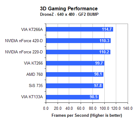
The gap gets a little wider here in DroneZ but still not large enough to start splitting hairs over. By this point it's pretty clear where the nForce's performance levels are.
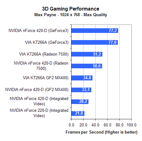
Overall Integrated Video & Gaming Performance
In order to test the integrated GPU of the nForce as well as offer more thorough gaming tests at resolutions greater than 640 x 480, we also ran another set of benchmarks. These numbers used the latest Detonator XP drivers to show you the type of performance you can expect from the two fastest Athlon platforms available today.
These tests made use of a 1.2GHz Athlon for better comparison with the 1.2GHz Palomino based Athlon MP results we will present in the section that follows this one.
Since we've already established that without the integrated video, the nForce 420 and 220 are identical in performance we've thrown out the 220 scores for this section to simplify the graphs somewhat.
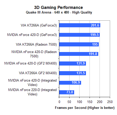
The inclusion of a Radeon 7500 in this test is just to prove that the card is indeed compatible and performs quite well on a NVIDIA based motherboard.
As you can see, the KT266A has a slight lead over the nForce but not enough to make a noticeable performance difference.
In spite of NVIDIA's initial claims that the integrated video of the nForce would be equivalent to or faster than a GeForce2 MX, it's clear that this isn't the case. A GeForce2 MX400 (or a regular GeForce2 MX for that matter) is about 22% faster than the integrated core on the 420-D because of memory bandwidth constraints. Remember that a regular GeForce2 MX has a full 2.7GB/s of memory bandwidth available to it; judging by these performance figures, the integrated GPU does not have a comparable amount.
When the memory bandwidth is cut in half by moving down to the 220-D, the bandwidth limitations even more thoroughly castrate the integrated GPU's performance.
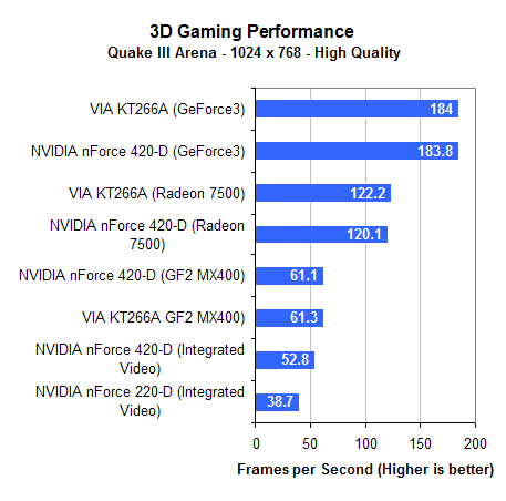
At 1024 x 768 the integrated GPU is not able to even break 60 fps with a 1.2GHz Athlon at the helm. The performance of the 220-D is even more dismal.
UnrealTournament
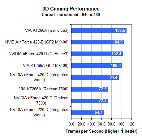
Under Unreal Tournament we see the same initial signs of the performance (or lack thereof) that's soon to come. The KT266A is about 7% faster than the nForce 420-D here.
Even at this low of a resolution, an external GeForce2 MX400 is a good 11% faster than the internal GPU of the nForce.
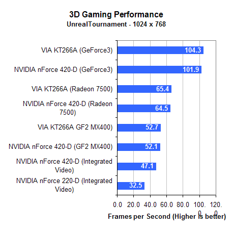
The trend continues here, but there is only a 10% difference in performance between the external GF2 MX400 and the integrated video on the nForce 420-D.
Max Payne
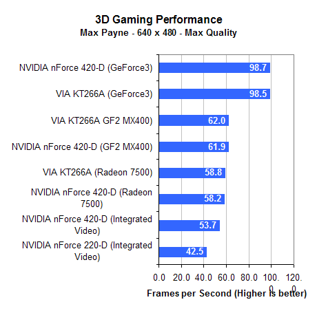
There's not much new under Max Payne except the performance difference between the 420-D with an external GF2 MX400 and with the integrated GPU enabled is now around 15 – 17% at the two resolutions we tested at.
The Effects of DASP on Palomino
A big question we asked ourselves when we were first introduced to nForce's built-in prefetching logic (DASP) is how it would complement (if at all) the data prefetch in AMD's Palomino core. In order to test this we chose a 1.2GHz Athlon processor and compared it to a 1.2GHz Athlon MP (Palomino core) on both the KT266A and nForce 420-D platforms. In theory, the performance improvement each platform gets from moving to the Athlon MP should be identical since all other variables are held constant. But if nForce's DASP indeed removes some of the benefit of the Palomino's data prefetch then the performance improvements shouldn't be identical.
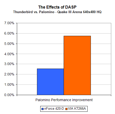
Quake III Arena ended up being the perfect test for this as the KT266A clearly showed that it benefited more from the Thunderbird > Palomino transition than the nForce. The only real explanation is that the IGP's DASP removes some of the usefulness of data prefetch provided by the Palomino core.
It is also worth noting that these results are not visible in all benchmarks, Quake III Arena is a special case because data prefetch improves performance under the game so much already.
Integrated Audio Performance
The recent release of the Creative Labs Audigy makes this comparison we're about to do a bit dated however once we are able to test its digital output capabilities we will revisit the audio solution and compare it to the Audigy. In the interest of time, we have kept this comparison to one of the nForce APU vs. the SB Live!
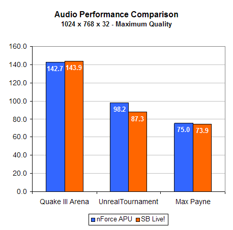
Other than under UnrealTournament, there aren't many significant performance differences between the nForce APU and the SB Live! in these games. The performance difference in UT is significant however and it should be noted that it's not present in UT's default 22 kHz mode but emerges as the sampling rate is increased to 44.1 kHz.
These next set of tests were all conducted with a 44.1 kHz sampling rate 16-bits.
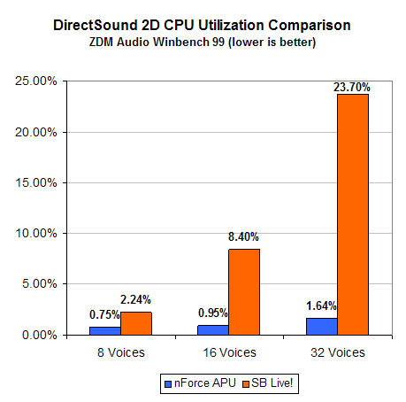
Audio Winbench is a very useful benchmark if you know to look at the right sets of numbers. Here we can see that the SB Live! is clearly not capable of offloading as many tasks from the CPU as the nForce APU. Normally we'd use a slower speed CPU to show the devastating effects of this but on our 1.2GHz Athlon, 23% CPU utilization just for audio processing is just too high.
It is worth noting that for most gamers, between 8 and 16 2D voices are common so those are the values you'll want to look at. Even then, 8.4% is getting quite high compared to what the nForce APU is capable of. As a reference point, the new Creative Labs Audigy performs much more in line with the nForce APU than with the SB Live!
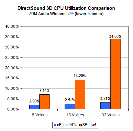
When dealing with 3D sound streams the CPU usage simply increases. Here, even with only 8 voices the SB Live! already eats up way too much of the CPU power for audio processing. With 32 voices, exactly 34% of the 1.2GHz Athlon is devoted to audio processing. It'd be interesting to see performance under 64 simultaneous voice conditions since the nForce APU can process up to 64 in hardware. You see, there's a reason that the nForce APU is capable of processing 6 billion instructions per second…
Final Words
If there was one phrase that would best summarize NVIDIA's nForce it would be "raising the bar," since that's exactly what it does. The introduction of the nForce and the subsequent assimilation into the market raises the bar in many areas; audio, video and integrated chipsets in general. Having something as powerful as the NVIDIA APU on every motherboard will quickly sour your taste on conventional AC'97 on-board audio not to mention what the next-generation nForce with an even more powerful integrated video core will do to the expectations for on-board video performance.
There are a couple of conclusions that can be made from this article. For starters, the performance of the nForce with an external AGP card is approximately on-par with that of the KT266A. While the KT266A does come out ahead in the majority of benchmarks, its lead is usually limited to 3% or less which is honestly indiscernible to even the most highly trained eyes. For the ultimate Athlon platform in terms of performance, the decision really comes down to the KT266A or the nForce. Assuming you're captivated by the features of the nForce, let's have a look at what your options are:
If you're not going to use the integrated video, the most sensible nForce solution to pursue is indeed the nForce 220-D. The reason motherboard manufacturers would want to push this solution is because the chipset is cheaper and physically laying out the board is not as difficult with only a single 64-bit memory bus to trace out on the PCB. At Computex we didn't see much emphasis placed on the nForce 220-D but we're hoping that the cost savings will be significant enough to see some support from motherboard manufacturers.
As ironic as it may be, the more expensive nForce 420-D is definitely more desirable if you want to go down the "cost effective" route and make use of the integrated video. Trying to play any of today's 3D games on a memory bandwidth limited nForce 220-D platform will not do the GPU or yourself any justice.
The nForce is a good platform for a user that's building a system from scratch since you do end up getting a very powerful sound processor and Ethernet controller in one package. For the user just casually upgrading their motherboard that already has money invested in a good sound card/Ethernet controller then there's not as much reason to move to nForce.
For an OEM looking for a highly integrated platform with all of the bells and whistles, the nForce fits the bill perfectly. It is all too often that we are forced to sacrifice quality or features when going with a highly integrated platform but the nForce changes all of that. Raising the bar is indeed what it does in this sense.
There's also the issue of price; NVIDIA was claiming that boards would retail in the $120 - $150 range and if we end up seeing a $120 nForce 220-D motherboard then we'd be quite pleased but we'll reserve judgment on that until we actually see boards available. Speaking of which, motherboards are going into mass production in October and you should see them shortly thereafter. As far as we know, MSI is currently closest to shipping boards out of all of the manufacturers.
So there you have it; the somewhat over hyped, somewhat misunderstood nForce. The product itself is very well designed, but we think NVIDIA will find it a little more difficult to dominate in the chipset market as well as they have in the video realm.


