Original Link: https://www.anandtech.com/show/781
 Rumors have been
circulating for quite sometime about NVIDIA's foray into the chipset market with
the Crush 11/12, but this year's Computex serves as the launch pad for the platform.
NVIDIA officially announced the chipset earlier today as the nForce and it's quite
possibly the biggest step forward in chipset technology we've ever seen.
Rumors have been
circulating for quite sometime about NVIDIA's foray into the chipset market with
the Crush 11/12, but this year's Computex serves as the launch pad for the platform.
NVIDIA officially announced the chipset earlier today as the nForce and it's quite
possibly the biggest step forward in chipset technology we've ever seen.
How was NVIDIA able to accomplish all of this with the release of their first chipset? Well they had a lot of help from friends in the industry that certainly made this happen much more quickly than would have otherwise been possible. Who you may ask? Well, the biggest asset in the development of nForce was clearly Microsoft. They, of course, gave NVIDIA close to $100 million to develop the core logic for the upcoming XBOX gaming console.
NVIDIA has wisely taken the technology they've developed for the XBOX and applied it to the PC market as well. Of course, NVIDIA can't just release the XBOX's chipset to the public because that would defeat the purpose of having an XBOX, which wouldn't exactly make Microsoft happy. What they have done is leverage some of the technologies used in the XBOX chipset but at a reduced performance level. Remember that the current specs for the XBOX are well beyond even the most advanced products available in the PC market at this time, so a "reduced performance level" may actually not be that bad.

Since the nForce is based closely off the XBOX chipset, that means it features graphics integrated into the north bridge. When most hardware enthusiasts see any mention of integrated graphics, they immediately turn their head. But with nForce, the integrated graphics really isn't that bad and, in fact, the technology in the rest of the chipset is so promising that you'll probably want this chipset in your system even if you upgrade to an external graphics card.
Ok, enough hype - let's take a look at what makes the nForce such an impressive product, at least on paper.
The Basics
The nForce chipset is made up of two parts, a north and south bridge, just like any other chipset. In accordance with NVIDIA's trend towards naming things as "processors," the north bridge is known as an Integrated Graphics Processor (IGP) while the south bridge gets the distinction of Media and Communications Processor (MCP).
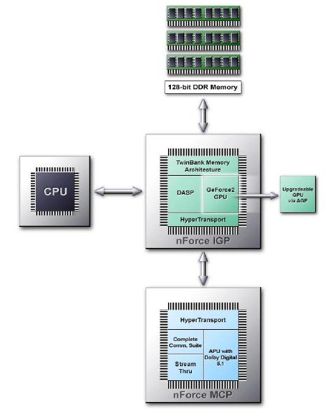
AMD's Hyper-Transport is used to link the two chips with much more bandwidth than any traditional chipset out there right now or on the horizon. At the same time, TwinBank memory architecture provides a 128-bit, 133 MHz DDR memory interface for a total of 4.2GB/s of memory bandwidth, also more than any traditional chipset.
Let's take a look at these individual components in depth to get an idea of what the nForce is really capable of.
Integrated Graphics Processor (IGP)
As the name suggests, the Integrated Graphics Processor (IGP) provides all the functions of a standard north bridge, including CPU interface, memory controller, and AGP interface, but also adds an integrated graphics core. That graphics core is very closely based on the NV11 core used in the GeForce2 MX, making it far more powerful than any other integrated graphics chipset on the market today or on the horizon.
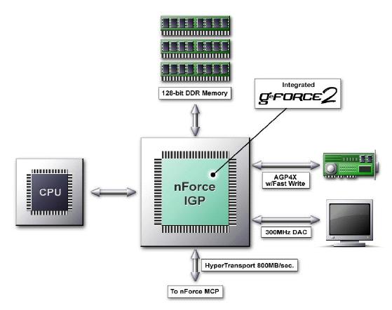
Like the GeForce2 MX, the nForce graphics core is clocked at 175MHz and features two pipelines, giving it a theoretical fillrate of 350 megapixels/sec. That also means we get a complete second generation transform and lighting engine. The kicker is that the graphics core gets an internal AGP 6X interface to the rest of the north bridge logic which could help tremendously in transferring things like triangle setup from the CPU to the graphics core's T&L engine or when the reserved frame buffer memory is used up and textures need to be swapped.
Of course, the biggest bottleneck in recent times for 3D graphics accelerators is memory bandwidth, which of course brings us to one of the most exciting features of the IGP - TwinBank Memory Architecture, which we'll talk about shortly. The combination of an integrated GeForce2 MX graphics core with TwinBank Architecture should put gaming performance in the neighborhood of a current DDR solution with an external AGP GeForce2 MX installed.
Remember that the integrated graphics on the nForce uses system memory, so 32MB of main memory is reserved at boot time for the frame buffer, although this may be a BIOS configurable option. The loss of system memory has always been one of the complaints some users have had about integrated graphics solutions, but with memory prices being so low today, this shouldn't be a major issue.
The IGP does also support an external AGP 4X slot, so those of you not interested in using the integrated graphics can just drop in another video card which will automatically disable the integrated video. Of course NVIDIA would like you to upgrade to a GeForce3, which does have some added benefit from a driver perspective, as we'll talk about in a bit.
However, this does bring up an interesting thought - would NVIDIA ever intentionally prevent other manufacturers graphics boards from working on their chipset? The chipsets are still too far from completion at this point in time to really find out, but it is something to think about it. With NVIDIA just getting into the chipset market, it probably wouldn't be the wisest move on their part to start off the with AGP compatibility issues. Nevertheless, if NVIDIA begins to take a large potion of the chipset market, it suddenly becomes very feasible for them to go this route in future chipsets.
TwinBank Memory Architecture
Like any other north bridge, one of the functions of the nForce IGP is providing the memory interface for the system. The IGP, however, goes a step further and offers a unique memory setup that NVIDIA likes to call TwinBank Memory Architecture. Basically, you get a 128-bit 133 MHz DDR memory interface, providing a total of 4.2GB/s of memory bandwidth - more than any other mainstream chipset on the market today.
While this is quite impressive, TwinBank is actually much more complex than just a dual PC2100 memory interface. In fact, the 128-bit memory bus is actually somewhat misleading - not because it's not really 128-bits wide, but because it doesn't tell the whole story. These 128-bits are actually divided up into dual-independent 64-bit memory buses, each with its own memory controller. This means that either the CPU or GPU can access either or both memory controllers, allowing for the most efficient use of memory bandwidth possible. This setup is precisely NVIDIA's Crossbar memory technology, first used in the GeForce3.
Of course, standard 184-pin DDR DIMM's are only 64-bits wide and NVIDIA has no interest in creating a new memory standard. As such, you'll have to install two DIMM's in an nForce 420 board to take advantage of TwinBank Architecture. The IGP-128 can fall back to 64-bit operation, at a performance hit of course, if only one DIMM is installed.
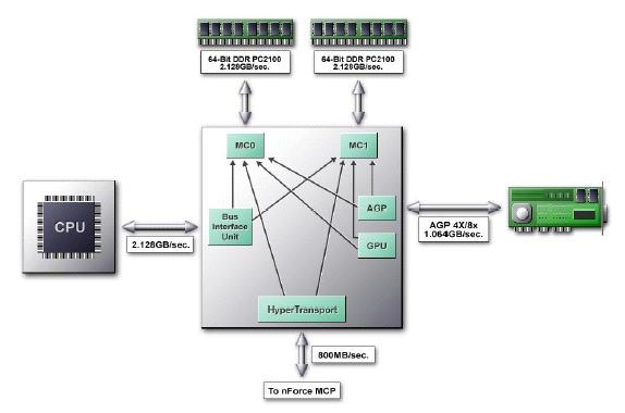
When we heard about the 128-bit memory interface on the nForce, we assumed that memory would have to be installed in matched pairs, but NVIDIA's tech docs state that this is not the case. Since each memory bank has its own memory controller, the modules can be different sizes and even different speeds. A Single Intelligent Arbiter decides which memory controller will handle what data. Nevertheless, our guess is that performance will be better if there is an equal amount of memory in each bank, since this will allow for the interleaving of data evenly between the two banks.
Interestingly enough, the IGP-128 supports 3 DIMM slots - an odd specification when there are two memory controllers. It turns out that the first slot is linked to the first memory controller and the other two slots are linked to the second memory controller. You'd think that the IGP would be able to support 4 DIMM slots with 2 in each bank, but obviously there was some sort of design issue that prevented them from doing this. We wouldn't be too surprised if some manufacturers come up with boards supporting 4 DIMMs. Once again, the memory controllers are completely independent of each other, so you can have unequal amounts of memory in each bank.
Note that there will be two version of the nForce IGP, one that supports the TwinBank 128-bit, 133 MHz DDR memory interface and one that only supports a standard 64-bit, 133 MHz DDR memory interface. The 128-bit model will be known as the IGP-128 and is included in the nForce 420 chipset, while the 64-bit model is the IGP-64 and is included in the nForce 220 chipset. Other than the memory interface, the two north bridges are identical.
Naturally, IGP-64 will have a lower pin count, making the chipset and boards cheaper to produce, but at a pretty hefty performance penalty. So far, we've yet to hear of an nForce 220 based product from any of the motherboard manufacturers, but they will undoubtedly come with time.
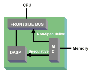
Dynamic Adaptive Speculative Pre-Processor (DASP)
 NVIDIA's come up
with quite a long name to describe one of the more interesting features of the
nForce IGP. NVIDIA described it best in their tech-docs:
NVIDIA's come up
with quite a long name to describe one of the more interesting features of the
nForce IGP. NVIDIA described it best in their tech-docs:
DASP is an intelligent agent that monitors CPU requests and looks for access patterns that it can successfully predict. When it recognizes such access patterns, it exploits unused memory bandwidth to load its cache with data the CPU is expected to request later. When the CPU requests the data, it is returned to the CPU immediately rather than after waiting for the memory access. For such requests, latency is reduced from 40% to 60%. DASP is carefully engineered to make efficient use of memory bandwidth while minimizing overall latency.
Basically, DASP acts much like the hardware prefetch found on the Pentium 4 and Palomino-based Athlon 4 processors. The difference here is that the feature is implemented on the north bridge, rather than on the CPU itself. As far as we know, this is another first for a chipset. In fact, NVIDIA claims that they've got a patent pending on the technology, so unless they license it out, we won't be seeing it on other manufacturer's chipsets anytime soon.
Interestingly enough, the i860 chipset from Intel apparently has a "prefetch cache" as well, but Intel is very tight lipped about it. Whether there is any similarity to NVIDIA's DASP has yet to be determined.
Of course, DASP will be most beneficial when the memory accesses can be predicted successfully, something that is most likely to happen with sequential or streaming access. Interestingly enough, these are the types of memory accesses in which RDRAM excels.
NVIDIA claims that DASP can boost performance up to 20%, but this seems to be primarily in raw memory benchmarks where DASP is most capable of correctly predicting the memory access pattern. Real world performance benefits look to be in the range of 5-10%, depending exactly what you're doing, with larger benefits coming in applications that stream a lot of data. This is about the same as the performance boost given by hardware prefetch on the Palomino-based Athlon 4.
The table below shows the performance numbers NVIDIA has achieved with DASP. Notice how streaming applications and memory benchmarks benefit the most, while office application benchmarks still receive a tangible benefit. The Sandra STREAM benchmarks are especially interesting and are quite a bit higher than the other DDR chipsets we've tested to date.
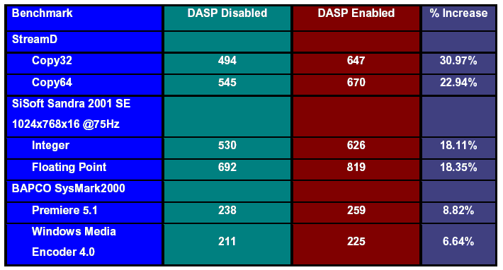
At this point, it appears that NVIDIA arrived at their numbers with a standard Thunderbird-based Athlon, so it's unclear how much DASP will help a processor that already has hardware prefetch, such as the Palomino-based Athlon 4.
Media and Communications Processor (MCP) & Audio Processing Unit (APU)
The nForce MCP provides all the standard south bridge features, including support for Ultra ATA 100, 6 USB ports, 10/100 Ethernet, 1/10 HomePNA, 56k modem and AC'97 sound. Unlike the integrated Ethernet found in recent Intel and VIA south bridges, it looks like most motherboard manufacturers will actually be taking advantage of this nForce feature.
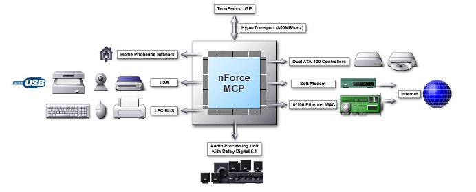
What differentiates the nForce MCP from other south bridges is the Audio Processing Unit (APU) NVIDIA has integrated into the chip. This will be the first fully DirectX 8 compliant audio part when it hits the market. The APU supports 64 3D voices or 256 2D voices in hardware, 32 hardware submixers, and is EAX 2 and I3DL2 compatible.
There are two versions of the MCP, with the difference being support for real time Dolby Digital AC-3 (5.1) encoding. This is by no means a trivial accomplishment and is the feature that distinguishes the MCP-D from the standard MCP. As such, the MCP-D is virtually identical to the MCPX found in the XBOX, but adds the PCI bus that a console has no need for. It seems that NVIDIA licensed the Parthus MediaStream DSP in order to integrate such a complex feature quickly enough to meet Microsoft's XBOX deadlines.
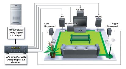
Dolby Digital AC-3 encoding means that you'll be able to digitally connect your computer to a home theater (or any other sound system) with a Dolby Digital Decoder and get sound quality that rivals a DVD movie - if done properly. If you choose not to use an AC-3 out, the APU can work with 2, 4, or 6 speaker configurations using standard analog interfaces.
The 4 billion operations per second of the MCP's DSP aren't used just to encode Dolby Digital on the fly, but also calculates occlusions, reflections, and HRTF functions, offloading these functions from the CPU. Thus, enabling 3D audio in games on an nForce-based system should not result in any slow down over standard stereo audio - at least in theory.
Right now, it's not clear whether or not the standard MCP will include fully hardware accelerated sound or if this will only come with MCP-D, but early indications are positive. It is clear, however, that Dolby Digital encoding will be limited to the MCP-D parts. So far, it seems that most of the motherboard manufacturers intend to include MCP-D on their initial boards, although this may change depending on the pricing of the chipset. Chipsets including MCP-D will have a "D" appended to their name, such as nForce 420D.
Connecting it all together - AMD's Hyper-Transport
nForce uses AMD's Hyper Transport protocol to connect the IGP and MCP components of the chipset. Hyper Transport was originally known as Lightning Data Transport (LDT) but was renamed earlier this year. The technology has been disclosed to over 100 manufacturers, NVIDIA being one of the larger players with access to the technology.
![]()
Hyper Transport is a very elegant dual ported serial link that can connect anything from a North Bridge and South Bridge (which is the case here) to two multiprocessor North Bridges.
The two ports on the bus link are used for incoming and outgoing traffic; they can each be between 2 and 32-bits wide. The implementation used in the nForce has a link width of 8-bits and an operating frequency of 200MHz. The bus is double pumped meaning that the effective transfer rate is equal to that of a 400MHz bus. This gives the nForce 400MB/s of bandwidth in any one direction or 800MB/s total bandwidth between the IGP and the MCP.
Should the need arise, NVIDIA can always increase the width of the Hyper Transport bus and/or increase the operating frequency but for now 400MB/s unidirectional bandwidth should be enough.
StreamThru
One feature of AMD's Hyper Transport bus is the ability to support multiple virtual channels. We believe that a particular implementation of this is what NVIDIA is calling StreamThru as a part of their nForce technology.
StreamThru basically guarantees that regardless of what other demands are placed on the chipset, the devices that are latency and bandwidth critical will receive the ultra fast access and bandwidth to main memory that they need in order to operate properly.
Devices that are latency and bandwidth dependent are known as isochronous devices, those that aren't latency dependent (meaning they can be interrupted for a bit in order to let another device occupy some time) are known as non-isochronous devices.
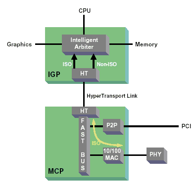
An example of an isochronous device is the integrated 10/100 network controller in the MCP. NVIDIA's internal architecture, made possible courtesy of Hyper Transport's support for virtual channels, will allow the 10/100 network controller to always get the bandwidth and low latency access to the graphics, CPU and main memory that it needs to operate without any interruption.
This is what NVIDIA is calling StreamThru but really the technology is made possible by Hyper Transport. It is useful nonetheless.
Bringing new meaning to the term "all in one"
NVIDIA is promising a single driver for all the components of the nForce chipset, including the integrated graphics, audio, Ethernet, HomePNA, busmaster IDE, chipset, etc. This of course makes setting up the drivers on an nForce system incredibly easy compared to any other chipset where the graphics, audio, chipset, busmaster, etc. drivers are not only independent from each other, but often come from different manufacturers.
One side benefit of this setup is that if you decide to upgrade with an NVIDIA-based graphics card, you won't have to install any new drivers if you already have the latest on your system.
Got boards? When?
Here at Computex, we've already seen quite a few nForce sample boards on display, mainly from the five launch partners, which include ABIT, ASUS, Gigabyte, MITAC, and MSI. They have been given exclusive rights to the chipset for the first few months of availability. These guys are all working closely with NVIDIA on the development of the boards and together have agreed upon a reference design that most of the manufacturers are following very closely.

The reference design that everyone is working with right now is a microATX form factor board. Only ASUS has deviated from the microATX form factor for their initial board, going instead with a standard ATX setup, although all the manufacturers assured us that standard ATX nForce boards would be available as well.

That reference design has 4 layers, which is exactly what motherboard manufacturers like to see since it keeps manufacturing costs down. Similarly, our sources tell us that NVIDIA is using a 0.15 micron 7-layer metal process to manufacture the nForce, which should help keep the cost and heat production down.

Apparently development of nForce boards has been quite rushed as we heard numerous times that designers started with essentially nothing about five weeks ago. Working samples were available to play with in private rooms at Computex; although we've been told performance and stability still need quite a bit of work, both in terms of motherboard and chipset designs. Fortunately, however, the word we're getting is that NVIDIA has been quite helpful in the design process and fully intends to have the boards be rock solid at the launch.

The current word is that evaluation samples will be ready later this month with the target for mass production being late August. If things go as they usually do, that could easily be pushed into September or even October, which is still quite a short period of time for a motherboard maker to go from nothing to retail quality boards.

I'm not a player, I just Crush a lot
With the launch of nForce, NVIDIA has made a major leap from being the top dog in the graphics business to a player in the intensely competitive chipset market. Without any prior experience, they've launched a chipset that appears on paper to be more powerful than anything on anyone's desktop chipset roadmaps at this point in time, making them an immediate threat to all chipset manufacturers right off the bat. And that's not even comparing to other integrated chipsets, but just chipsets in general. The nForce absolutely demolishes anything with integrated video here now or in the foreseeable future.
At the same time, they're only launching the nForce with support for AMD's EV6 bus, which then becomes a major selling point for AMD's Socket-A processors, especially in OEM systems where this will be immensely popular.
This is despite the fact that NVIDIA has obviously already designed a similar part compatible with Intel's GTL+ since the XBOX uses a Pentium III processor. Whether NVIDIA will launch a GTL+ version of the nForce sometime in the future is unclear right now.
In fact, NVIDIA's presentation of the chipset offered an interesting jab at Intel that went as follows: "NVIDIA's DASP technology dramatically enhances CPU performance well beyond other X86 architectures - even those with substantially higher 'published' core frequencies."
Meanwhile, by launching an APU that's the first fully DirectX 8 compliant audio part is a direct attack on all the sound card manufacturers out there. Add in the fact that they're the first with the ability to encode Dolby Digital AC-3 on the fly and NVIDIA is suddenly worlds ahead of everyone in the sound field as well.
It'll be interesting to see how this all plays out, because right now, NVIDIA probably has raised plenty of eyebrows around the industry. The idea of an almost all NVIDIA PC suddenly seems like a very real reality. In fact, the NVIDIA of today sounds a lot like the Intel of a few years ago.
Final Words
NVIDIA is taking an interesting approach to the chipset market with their first product in this space. They're going with a high-end integrated solution, which almost sounds contradictory at first thought.
Pricing of the chipsets still has not been set by NVIDIA, which of course means that prices for complete boards is not available yet either. That's yet another result of the rush to get nForce out so quickly. However, our estimates put board level products at under $200.
While this may at first that may seem a bit pricey for a motherboard, remember that you're getting the most advanced desktop chipset available today with the most advanced audio right on board. Consider the integrated GeForce2 MX a freebie - just forget about it if it's not fast enough for you. If you do plan to use the integrated graphics with an AMD CPU, then an nForce board is the perfect solution for building a relatively low cost, but still powerful gaming PC.
All we can say to the rest of the computer industry is "be afraid, be very afraid - NVIDIA is on the loose."


