Original Link: https://www.anandtech.com/show/604
Intel's NetBurst Architecture - The Pentium 4's innards get a name
by Anand Lal Shimpi on August 20, 2000 9:39 PM EST- Posted in
- CPUs
AMD has steadily been gaining market share ever since the release of their Athlon last August, their Thunderbird last June and their Duron shortly thereafter. The company has come from a microprocessor manufacturer that focused on supplying processors for the value market segment to a manufacturer that is helping to drive the desktop market in both performance and value segments.
One of the main reasons that AMD's recent processor releases have been so successful is because, unlike their competition, primarily Intel, the K7 architecture and its derivatives are free from the numerous limitations that 5-year old P6 architecture imposes on Intel's current flagship, the Pentium III. By reading the above statement, you'd assume that the Athlon was all but demolishing the Pentium III in terms of performance. Well, it's not.
The beauty of the K7 architecture is that it is very scalable, especially when you consider the largely untapped (by AMD of course) high-end workstation/server market that demands multiprocessor solutions. So while the Pentium III and its accompanying P6 bus are performing just fine now, there is a definite need for a more powerful solution for Intel's future processors if they plan on holding their current market advantage.
Intel gave us a very pleasant surprise at the Spring 2000 Intel Developer Forum (IDF) in February: for the first time the Willamette's architecture was discussed in a decent amount of detail. However, Intel has remained fairly quiet about the Willamette until now.
In two days, Intel's annual Fall IDF will commence, and the big topic of the day will be the architecture upon which the Willamette, or Pentium 4, is based. We were given the go ahead by Intel to let you all in on the details of this new architecture today so you can get a head start on your IDF reading, which we will be providing later this week.
A lot of what we will be talking about in this article is a follow-up to our initial IDF coverage in our Intel IDF Report #1 and our IDF CPU Report articles that were published earlier this year.
Intel's NetBurst Micro-Architecture
The P6 architecture, first introduced with the Pentium Pro in 1995 has been the basis for Intel's processors ever since then. The Pentium II, the Celeron, the Pentium III and even the newest Celerons all have their foundations in an architecture that has hit the 5-year old mark. As we described back in February, the Pentium 4 will be the first IA-32 (32-bit Intel Architecture) processor from Intel to use a non-P6 architecture in recent times.
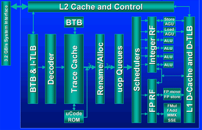
Today, that architecture gets a name and like many of today's Internet driven
products, you can see similar roots in its name. Of course, we're talking about
Intel's NetBurst Architecture.
The NetBurst Architecture is simply the name given to the Willamette architecture we discussed in our IDF coverage 6 months ago.
Hyper Pipelined Technology
The NetBurst architecture's first feature is what Intel is calling its Hyper Pipelined Technology, which is a fancy term for the 20 stage pipeline that the Pentium 4 has. This 20 stage pipeline is twice as long as the 10 stage P6 pipeline that the Pentium III featured and four times as long as the P5's five stage pipeline. A longer pipeline, as we've explained before, has its pros and cons.
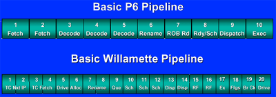
The 20-stage pipeline on the Pentium 4 is what allows it to hit higher clock speeds right off the bat without requiring a die shrink. It is for this reason that the Pentium 4 will debut at speeds of 1.4GHz and higher (we will talk more about clock speed in a bit). Before you let that number impress you too much, you have to realize that the 20-stage pipeline of the Pentium 4 also yields what is called a lower amount of Instructions Per Clock (IPC). A lower IPC basically means that you get less accomplished in a given amount of time when compared to a processor that has a higher IPC - pretty simple right?
Well, there are a number of ways you make up for a lower IPC; one of the most obvious is to simply increase the clock speed, which Intel is definitely doing in this case. There isn't a doubt that on any of the current benchmarks, if a 1GHz Pentium III were put up against a hypothetical 1GHz Pentium 4, the Pentium III would win because it can do more per clock than the Pentium 4.
By the time the Pentium 4 hits the streets, the fastest Pentium III will most likely still be the 1.13GHz part we reviewed not too long ago, and with the P4 debuting with at least two speed grades (1.4GHz and above is Intel's official statement, but also remember that we saw a 1.5GHz Pentium 4 in February) there should be a performance delta between the two upon its launch.
Modern day CPUs attempt to increase the efficiency of their pipelines by predicting what they will be asked to do next. This is a simplified explanation of the term Branch Tree Prediction. When a processor predicts correctly, everything goes according to plan but when an incorrect prediction is made, the processing cycle must start all over at the beginning of the pipeline. Because of this, a processor with a 10 stage pipeline has a lower penalty for a mis-predicted branch than that of a processor with a 20 stage pipeline. The longer the pipeline, the further back in the process you have to start over in order to make up for a mis-predicted branch. The second problem presented with a longer pipeline is that the penalties for a mis-predicted branch are much greater than in a shorter pipeline.
In order to navigate around these problems, Intel's NetBurst architecture has a few features that help to lessen the burden of having a longer pipeline.
Rapid Execution Engine
As we mentioned in our initial coverage of the CPU, the Pentium 4's Arithmetic Logic Units (ALUs) operate at twice the core clock frequency. This means that on a 1.4GHz Pentium 4, the ALUs are effectively running at 2.8GHz and on the 1.5GHz Pentium 4 demo we saw 6 months ago, the ALUs were effectively running at an impressive 3.0GHz. Intel refers to this feature as the NetBurst architecture's Rapid Execution Engine.
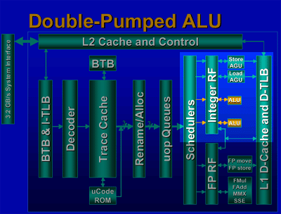
We predicted that this would give the Pentium 4 the clear advantage in Integer performance, however from our recent discussions with Intel, it seems as if the main reason for clocking the integer ALUs at twice the core frequency was to make up for the lower IPC of the NetBurst architecture.
While we can't release performance numbers today (those will have to wait until the CPU is actually released), remember that the Rapid Execution Engine might be necessary in order to make sure that the Pentium 4 can outperform the Pentium III in integer applications.
The biggest question most of you all had when we first mentioned the 2X clocked ALUs back in February was whether or not we'd see chips advertised at 3GHz just because their ALUs were effectively running that high or whether we'd see some processors with normally clocked ALUs and others with 2X ALUs. Our understanding of the matter is that Intel won't be doing anything like that, and the feature is simply a part of the NetBurst architecture. It would be very misleading if Intel attempted to pursue either of those avenues of marketing, and chances are that they won't.
The Pentium 4's Cache
The second method of combating the problems associated with mis-predicted branches that could occur within the Pentium 4's 20-stage pipeline is by using what Intel calls the Execution Trace Cache. We mentioned this Trace Cache when we first had a look at the architecture, but we're finally able to provide you with some more information regarding the L1 cache and how Intel is positioning it.
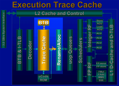
First of all, let's take a quick look at what the Execution Trace Cache does:
The decoder of any x86 CPU (what takes the fetched instructions and decodes them into a form understandable by the execution units) has one of the highest gate counts out of all of the pieces of logic. This translates into quite a bit of time being spent in the decoding stage when preparing to process an instruction either for the first time or after a branch mis-prediction.
The Execution Trace Cache acts as a middle-man between the decoding stage and the first stage of execution after the decoding has been complete. The trace cache essentially caches decoded micro-ops (the instructions after they have been fetched and decoded, thus ready for execution) so that instead of going through the fetching and decoding process all over again when executing a new instruction, the Pentium 4 can just go straight to the trace cache, retrieve its decoded micro-op and begin execution.
This helps to hide the penalties associated with a mis-predicted branch later on in the Pentium 4's 20-stage pipeline. Another benefit of the trace cache is that it caches the micro-ops in the predicted path of execution, meaning that if the Pentium 4 fetches 3 instructions from the trace cache they are already presented in their order of execution. This adds potential for an incorrectly predicted path of execution of the cached micro-ops however Intel is confident that these penalties will be minimized because of the prediction algorithms used by the Pentium 4.
Intel is abandoning the common method of defining cache size, at least for the Execution Trace Cache. Instead, they are stating that the trace cache can cache approximately 12K micro-ops. Since we don't have any other architectures quite like this, we can't really offer a comparison for that number. In addition to the L1 Execution Trace Cache, the Pentium 4 features an 8KB L1 Data Cache. If you're big on processor specs, you'll realize that this is smaller than the Pentium III's current 16KB L1 Data Cache. According to Intel, this size sacrifice was made in order to achieve a better price/performance ratio for the Pentium 4 in respect to the cost of the additional die size/transistors versus the performance an additional 8KB would offer.
The Pentium 4 will also feature a 256KB L2 cache running at the processor's core clock speed. This L2 cache will feature a much higher bandwidth than the current 256KB L2 on the Pentium III, partly because of the fact that the Pentium 4 will be running at a higher clock speed but also because of the fact that data is transferred on every clock as opposed to every other clock with the Pentium III's cache.
In terms of the bandwidth available to and from the L2 cache, a hypothetical Pentium III clocked at 1.5GHz would have 24GB/s of available bandwidth to and from the L2 cache, while a Pentium 4 clocked at the same speed would have 48GB/s of available bandwidth because it is able to transfer data on every clock.
This is one area where the Athlon (Thunderbird) has a disadvantage, because the chip features a 64-bit path to its L2 cache whereas the Pentium III/4 feature a 256-bit datapath to its L2 cache.
Just as with the Pentium III, all of the Pentium 4's L1 cache (including the Execution Trace Cache) will be duplicated in its L2 cache.
The Pentium 4's Chipset & Bus
The move to a 133MHz FSB helped the Pentium III remain competitive with the Athlon, as we've seen from the benchmarks, but in order to handle future applications, there is a definite need for a larger amount of system bandwidth. This necessity is accomplished by the quad-pumped bus that will be the backbone for the Pentium 4's transactions.
The 100MHz FSB is quad-pumped, meaning it yields transfer rates equivalent to that of a 400MHz FSB clock (3.2GB/s). This will give Intel, for the first time since the release of the Athlon and its 200MHz EV6 bus, the advantage over AMD in terms of available system bandwidth. Also remember that although AMD's EV6 bus is easily scalable to 400MHz as well, they haven't seen a need for that boost as of now.
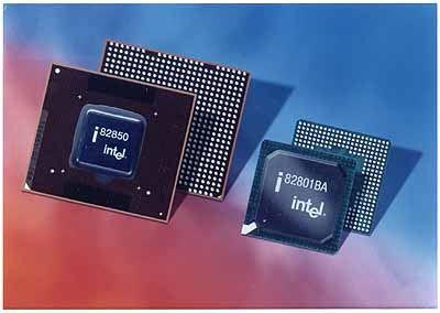
As we mentioned last time, the Pentium 4 will run on Intel's upcoming Tehama chipset, which has since been dubbed the i850. The i850 won't offer any significant enhancements to Intel's Hub Architecture, it will pretty much be a single processor version of the i840 chipset with support for the Pentium 4's bus.
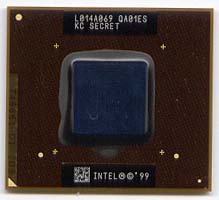
Intel's i850 Memory Controller Hub
Because it has its roots in the i840 chipset, the i850 will feature a dual channel RDRAM memory setup. Unfortunately, RDRAM prices are still not on par with SDRAM prices; combine that with the fact that you will have to install RDRAM RIMMs in pairs on i850 boards (because of the dual channel RDRAM setup) and you are talking about a noticeable price increase simply because of the fact that the i850 chipset only supports RDRAM. Since the MTH is, thankfully, gone, there won't be any SDRAM solutions for the Pentium 4 from Intel until the second half of 2001. This could very well hurt Pentium 4 sales, at least in terms of the hardware enthusiast community's willingness to adopt a processor whose only available platform is an RDRAM only solution. If RDRAM prices don't fall even more, it would definitely be in Intel's best interest to explore the possibility of releasing their SDRAM based P4 chipset earlier than the second half of next year.
While there has been a lot of talk about VIA producing a Pentium 4 chipset, they currently do not have a license to do so. We'll have to wait and see if they can produce a SDRAM based solution for the Pentium 4 before Intel's own chipset.
AMD took advantage of the fact that Intel's flagship platform was and still is the i820. If the acceptance of RDRAM continues to be as low as it has been, the i850 may be a tragic flaw of the Pentium 4, at least for the first few months of its existence.
The P4's bus, unlike the Athlon's EV6, isn't a Point-to-Point bus, meaning that all CPUs must share the same 3.2GB/s of available system bandwidth. With a Point-to-Point bus, although it's more complicated to implement, each CPU in a multiprocessor environment gets its own connection to the North Bridge meaning that in the case of the Athlon's EV6 bus, each CPU in a multiprocessor setup would get a 200MHz connection to the North Bridge.
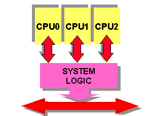
Point-to-Point Bus Protocol
- AMD EV6
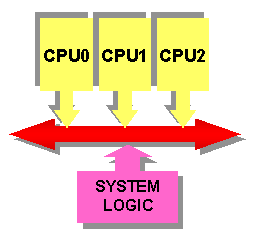
Shared Bus Protocol -
Intel NetBurst Bus
Intel also informed us that the Pentium 4 would strictly be a uniprocessor part, meaning it won't even work in multiprocessor boards. We'll have to wait for the SMP version of the CPU, currently called Foster, before we can see what the Pentium 4 can do in a multiprocessor environment. Its 400MHz FSB should help considerably in dual processor systems which are currently forced to share a 100MHz FSB, at least on Intel platforms.
The chip, SSE2 & Heat
Intel hasn't revealed any more information about the Pentium 4's SSE2 instructions, although we do know that from our experience with the game, Shiny's Sacrifice will be able to take advantage of SSE2. For more information on SSE2, take a look at our Spring IDF 2000 coverage.
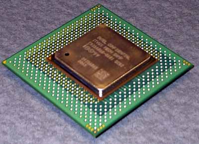
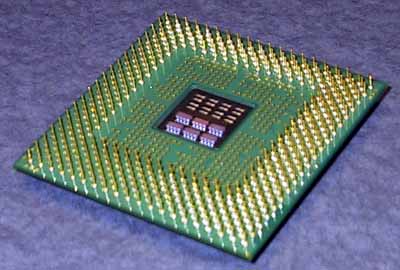
The 432-pin Pentium 4 should dissipate around 52W of heat when operating at launch speeds; this puts it below that of the 1GHz Thunderbird that is currently available.
Conclusion
As the Pentium 4's release approaches, the tension mounts to see how Intel's Pentium 4 will compete against AMD's upcoming Mustang core. Another interesting topic of discussion will be how big of an effect RDRAM will have on the Pentium 4's launch. Intel is still committed to pairing up the P4 with its dual RDRAM channels, and even when they do release a SDRAM based chipset for the P4, the i850 will still remain as the processor's suggested platform.
The CPU industry is obviously about to get very competitive -- as if it weren't competitive enough already.

