Original Link: https://www.anandtech.com/show/568
Intel’s Celeron has been boasting its new Coppermine128 core for just under three months now, and for most of that time, the CPU has received a decent amount of support from hardware enthusiasts, especially those that don’t have any moral objections to overclocking.
While the majority of the PC purchasing population could view the Celeron as an extremely crippled version of Intel’s Pentium III, most AnandTech readers could also see the Celeron in a different light: as a processor that helped prove that value doesn’t have to mean slow.
Deliberately held back by its 66MHz FSB and using clock multipliers of 8.0x and higher, the Celeron actually turned out to be the perfect candidate for overclockers since, by simply increasing the FSB from 66MHz to 100MHz, you’d have an 800 – 900MHz Celeron that didn’t have the same limitations of the 66MHz FSB parts.
Unfortunately, one thing we noticed with the Celeron was that although it could be overclocked to pretty much the same levels that the Pentium III was being shipped at (meaning that 533 – 600MHz parts could hit 800 – 900MHz), on a performance comparison basis, the Celeron was losing to equivalently clocked Pentium IIIs.
While we originally attributed this to the fact that the Celeron had 1/2 the L2 cache of the Pentium III, it later became known that it wasn’t the fault of the L2 cache but rather the fact that it was only a 4-way set associative L2 cache in comparison to the Pentium III’s 8-way set associative L2 cache, which allows the Pentium III’s L2 cache to achieve a higher hit rate than the L2 cache on an equivalently clocked Celeron.
This allowed AMD’s Duron, which turned out to be almost as fast as the original Athlon, to come in and completely dominate the “value” market.
Just days after the very successful launch of AMD’s Duron, Intel is back with three more clock speeds to add to their Celeron line. Remember that in the retail market, the processor war is fought with clock speed, not necessarily with overall performance. Now available at clock speeds of up to 700MHz, it’s time for Intel’s Celeron to truly go head to head with AMD’s recently released Duron.
While it’s always nice to look at the Ferraris and the Porsches in the magazines, when it comes down to it, there are more affordable family sedans and coupes on the roads than anything else. In the value processor market, the question is whether you’ll be seeing an “Intel inside” or a “Powered by AMD’s Duron” logo on the streets.
Before getting into the performance comparison, let’s have a quick look at what makes the Celeron what it is today.
The Basics
Today’s Celeron is a little different than the Celerons that were around not too long ago. Ever since after the release of the Celeron 533, the Celeron has been manufactured using a different core. While everything prior to the Celeron 533A and the 566 had been manufactured using the 0.25-micron Mendocino core (128KB on-die L2, no SSE) the last few Celeron releases have been of processors that feature the new Coppermine128 core.
As we described in our original Celeron “Coppermine128” review, the main differences between the Coppermine128 core and the Mendocino core exist in the fact that the Coppermine128 core features the same SSE instructions that have been with the Pentium III since the Katmai core and it also features the same 256-bit data path to its L2 cache as the newer Pentium III “Coppermine” that it is derived from.
The Coppermine128 is manufactured by essentially taking a regular Pentium III based on the Coppermine core and disabling half of the L2 cache. This can be verified by looking at the die sizes for both the Coppermine128-based Celerons and the Coppermine Pentium IIIs (they are equal). The reason Intel does this is because there is no guarantee that when they produce a Pentium III with 256KB of L2 cache on-die that all of that 256KB L2 will be functional and fit for sale as a part of a processor. In the event that some of the 256KB L2 fails the required production tests, Intel can simply disable 1/2 of the L2 and re-label the part as a Celeron after changing the clock speed and FSB pins of the CPU.
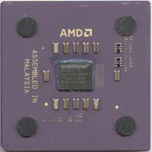
AMD's Duron
Now AMD goes about this problem in an entirely different way. They simply duplicate the number of L2 cache columns and if there is a particular block that fails production tests then AMD can simply disable the entire column. It is because of this that the Thunderbird and Duron are actually two different dies.
But let’s get back to the Celeron. Because the Celeron is basically a Coppermine core with 1/2 of the L2 cache disabled, the Celeron also loses half of the associativity of the Coppermine’s L2 cache, meaning the processor features a 4-way set associative L2 cache versus the 8-way set associative cache on the Pentium III. This actually hurts the Celeron more than you would think as it dramatically decreases the hit rate of the processor’s cache.
Combined with the fact that the Celeron is still limited by the 66MHz FSB and its 66MHz memory bus and you have a part that is significantly slower than an equivalently clocked Pentium III, Athlon, Duron or Thunderbird.
|
CPU
Specification Comparison
|
||||||||
|
AMD
Duron
|
AMD
Athlon
|
Intel
Pentium III
|
Intel
Celeron
|
|||||
| Core |
Spitfire
|
K7
|
K75
|
Thunderbird
|
Katmai
|
Coppermine
|
Mendocino
|
Coppermine128
|
|
Clock Speed |
600
- 700 MHz
|
500
- 700 MHz
|
750
- 1000 MHz*
|
450
- 600 MHz
|
500
- 1000 MHz
|
300
- 533 MHz
|
533
- 700 MHz
|
|
| L1 Cache |
128KB
|
32KB
|
||||||
| L2 Cache |
64KB
|
512KB
|
256KB
|
512KB
|
256KB
|
128KB
|
||
| L2 Cache speed |
core
clock
|
1/2
core
|
2/5
or 1/3 core
|
core
clock
|
1/2
core
|
core
clock
|
||
| L2 Cache bus |
64-bit
|
256-bit
|
64-bit
|
256-bit
|
||||
| System Bus |
100 MHz DDR (200 MHz effective) EV6
|
100
- 133 MHz GTL+
|
66
MHz GTL+
|
|||||
| Interface |
Socket-A
|
Slot-A
|
Socket-A
Slot-A (OEM only) |
Slot-1
|
Slot-1
Socket-370 |
Socket-370
|
||
| Manufacturing Process |
0.18
micron
|
0.25
micron
|
0.18
micron
|
0.25
micron
|
0.18
micron
|
0.25
micron
|
0.18
micron
|
|
| Die Size |
100mm^2
|
184
mm^2
|
102mm^2
|
120mm^2
|
128mm^2
|
106mm^2
|
153mm^2
|
106mm^2
|
| Transistor Count |
25
million
|
22
million
|
37
million
|
9.5
million
|
28
million
|
19
million
|
28
million
|
|
* Note: The K75 core actually took over the entire Athlon line and was available in 500 - 750MHz versions as well although it launched at 750MHz. The Thunderbird, although officially launched at 750MHz is available at speeds lower than 750MHz but only as OEM parts.
The Celeron's Limitations
For a full investigation of exactly how much the Celeron's 66MHz FSB and its 66MHz memory bus limit the processor's performance take a look at our original Celeron "Coppermine128" Review. But for a brief recap of the conclusions we came to here are some quick comparisons of the effects of the 66MHz memory bus and FSB on the Celeron's performance:
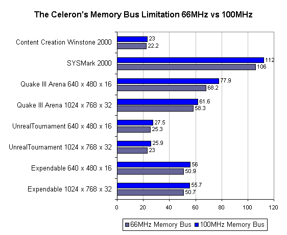
As you can see there is a noticeable performance difference between running a Celeron with a 66MHz memory bus and running it with a 100MHz memory bus. The largest differences come up under Quake III and under SYSMark 2000 as well.
In order to measure the effects of the 66MHz FSB on the Celeron we were forced to disable the L2 cache of both a Pentium III and a Celeron and left them at equivalently clocks, the difference between the two being that the Celeron was using a higher multiplier and a 66MHz FSB while the Pentium III made use of a 100MHz FSB to reach the same frequency with a lower clock multiplier. While this did exaggerate the effects of the 66MHz memory bus in particular, it does help us to get our point across that it is a definite limitation of the Celeron.
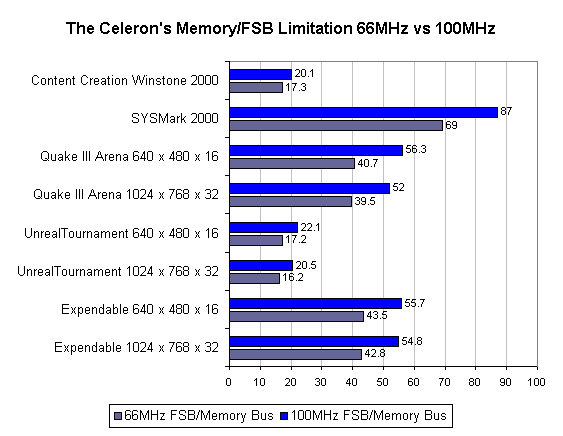
Factoring in the 66MHz FSB into the equation leaves the Celeron even more penalized under SYSMark and Quake III Arena and it continues to feel the pain under the other tests as well.
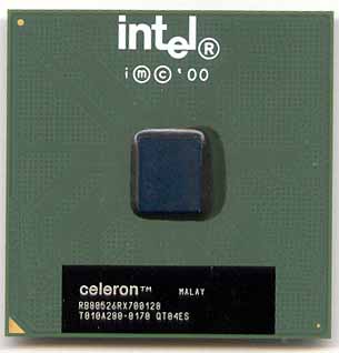
Celeron 700 Specifications
· 0.18-micron Coppermine128 core
· 700MHz clock speed – 10.5x clock multiplier
· 32KB on-die L1 cache running at core speed
· 256-bit Advanced Transfer Cache – 4-way set associative 128KB on-die L2 cache running at core speed
· Advanced System Buffering
· 370-pin FC-PGA Socket-370 GTL+ CPU interface running at 66MHz
· 1.65v core voltage
The Celeron 700 is really no different from the 566/600MHz parts that have been on the streets for a while now. It is still based on the same 0.18-micron Coppermine128 core, features the same amount of L1 cache (16KB Instruction + 16KB Data cache) and the same 128KB inclusive L2 cache.
The only major difference is that Intel increased the core voltage of the Celeron by 10%, from 1.50v of the 533 – 600MHz parts to 1.65v, which happens to be the core voltage of most of the Pentium IIIs as well.
Most overclockers are also familiar with this practice. If your CPU isn’t completely stable at a higher clock speed simply give the core voltage a little boost to see if things get better. Since 1.65v is still within the range of tolerance for the Celeron it seemed easiest for Intel to just increase the core voltage of the CPU in order to hit 700MHz instead of having to introduce a new core stepping to achieve the same effect.
The downside to this is that if you’re interested in overclocking the new Celeron 700 you’re not going to have as pleasant of an experience as you might have had with the 1.50v variants such as the 566MHz and 600MHz parts since the CPU is already running at a much higher core voltage.
Overclocking
Our particular Celeron 700 wouldn't run reliably at any overclocked speed other than 840MHz which was obtained using the 80MHz FSB speed which is still slower than the 850/100MHz overclock we obtained with the Celeron 566. Even raising the core voltage to 1.75v wouldn't help push the limits of the processor any further.
The Test
Note: The BX platform running at 133MHz FSB and the Celeron running at 100MHz FSB are both overclocked platforms and are not sold in that form on the retail market. Those performance numbers are only included for purposes of remaining thorough with our comparison.
Note 2: The i815 & VIA 133A platforms had the memory bus running at 100MHz while the FSB was running at 66MHz.
|
Windows 98SE / 2000 Test System |
||||||
|
Hardware |
||||||
|
CPU(s) |
Intel
Pentium III 800E |
Intel
Pentium III 800
Intel Pentium III 733 Intel Pentium III 667 Intel Pentium III 600EB |
AMD
Duron 700
AMD Athlon (Thunderbird) 800 AMD Athlon 800 AMD Athlon 700 AMD Athlon 600 AMD Athlon 500 |
|||
| Motherboard(s) | AOpen AX6BC Pro Gold | AOpen AX6C | ASUS CUSL2 (815) | ASUS P3V4X | VIA
KT133 Reference |
ASUS K7V |
| Memory |
128MB PC133 Corsair SDRAM |
128MB
PC800 Samsung RDRAM
|
128MB
PC133 Corsair SDRAM
|
128MB
PC133 Corsair SDRAM
|
||
| SDRAM CAS Latency |
CAS2 |
N/A
|
CAS2
|
|||
| Hard Drive |
IBM Deskstar DPTA-372050 20.5GB 7200 RPM Ultra ATA 66 |
|||||
| CDROM |
Phillips 48X |
|||||
| Video Card(s) |
NVIDIA GeForce 2 GTS 32MB DDR (default clock - 200/166 DDR) |
|||||
| Ethernet |
Linksys LNE100TX 100Mbit PCI Ethernet Adapter |
|||||
|
Software |
||||||
|
Operating System |
Windows
98 SE |
|||||
| Video Drivers |
|
|||||
|
Benchmarking Applications |
||||||
| Gaming |
GT
Interactive Unreal Tournament 4.20 AnandTechCPU.dem |
|||||
| Productivity |
BAPCo SYSMark
2000 |
|||||
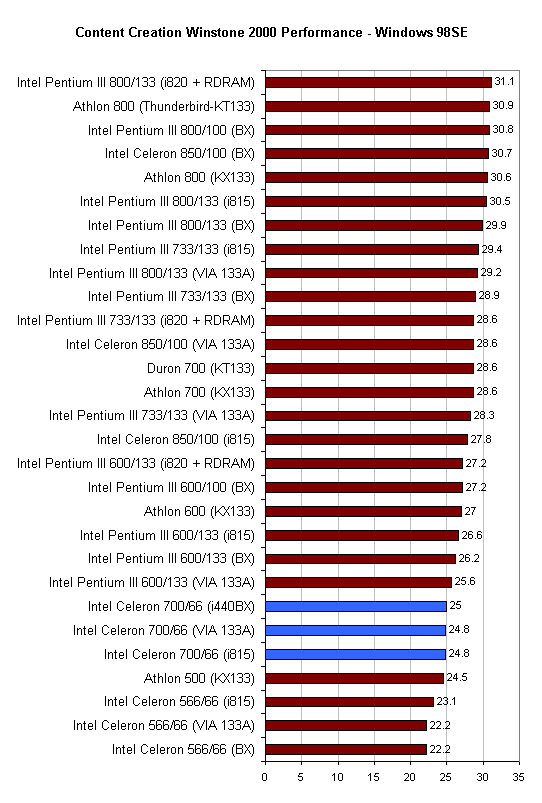
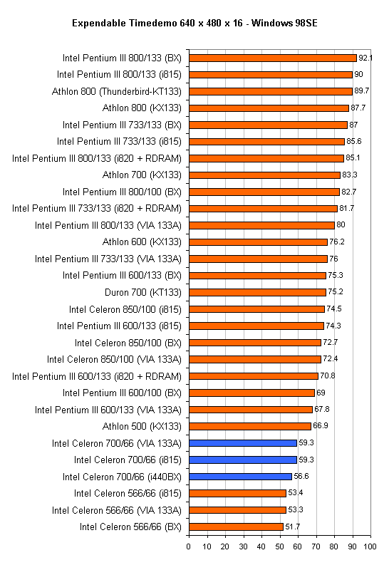
As you can see, at 700MHz the improvement the Celeron offers over the 566MHz part we looked at in March is next to nothing. The Celeron 700 is clearly a "low-end" solution and is easily outperformed by a Pentium III 600, not to mention that a Duron 700 is definitely much faster of a CPU.
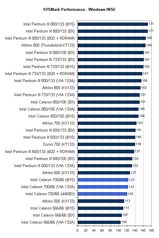
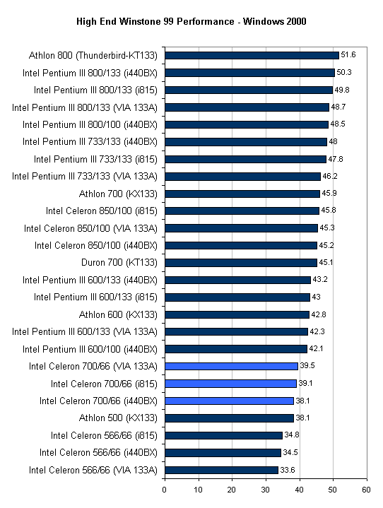
The standings change very little when we move to SYSMark 2000, the Celeron 700 is still obviously limited by its FSB and its memory bus both at 66MHz and are barely outperforming the Athlon 500.
The 23% increase in clock speed over the Celeron 566 results in barely over a 10% increase in performance which clearly shows you that there is a limitation that is preventing performance from scaling linearly with clock speed. We already proved what those limitations were, the FSB and memory frequency.
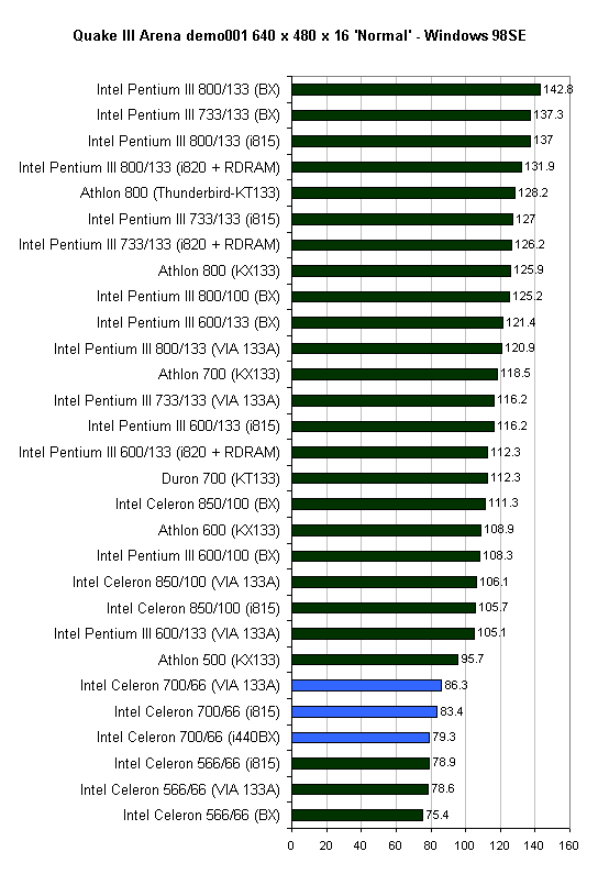
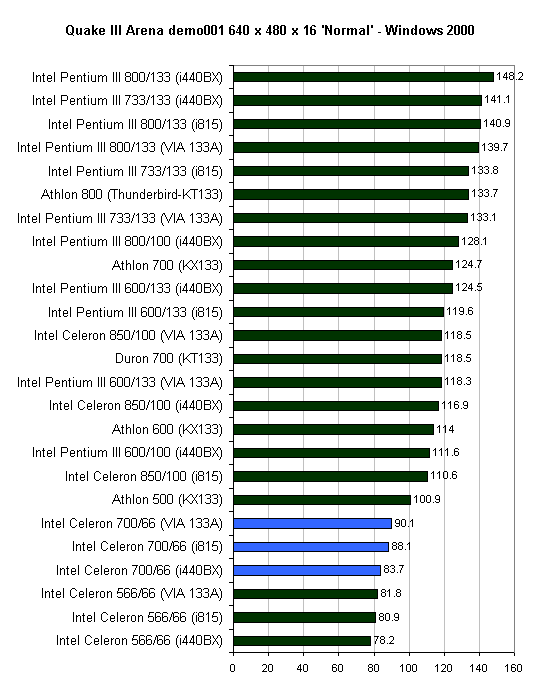
Now as we switch to Quake III it becomes very clear that the Celeron isn't exactly your best gaming solution either. In this case a Celeron 700 isn't even able to compete with an Athlon 500.
It is interesting to note that the Celeron 700 running on the VIA 133A platform is actually faster than the same configuration on a i815 platform. While it's not by much it is definitely there. The reason the BX platform comes in last is because both the i815 and VIA 133A setups allow the memory clock to be set at 100MHz while the FSB is set to 66MHz while the BX only allows a 66/66MHz configuration.
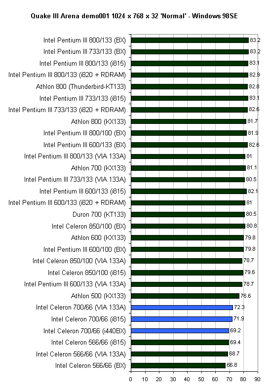
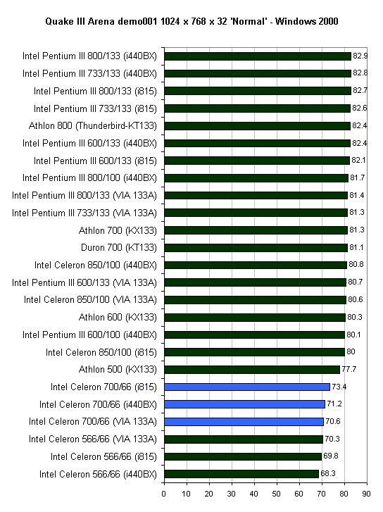
At 1024 x 768 x 32 where the video card should obviously be a limitation the scores should be within a couple of percent of one another. But with the Celerons you notice that the scores are a bit lower than the norm. This is because the 66MHz FSB/memory bus is holding their performance back in addition to the video card memory bandwidth limitations.
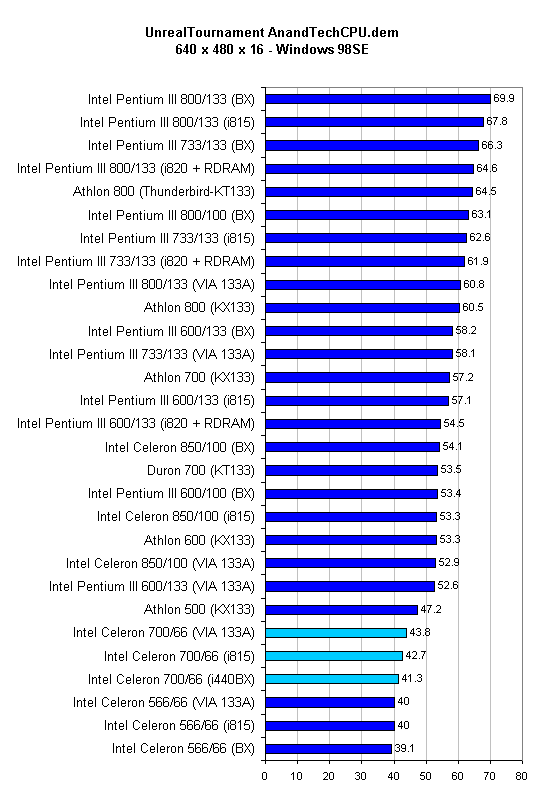
Under UnrealTournament the performance standings are pretty similar as well, the last six spots are held by the Celeron 566 and 700. Once again the fastest platform for the Celeron seems to be the 133A with the memory running at 100MHz, and it is cheaper than the i815 because you aren't paying for the integrated video of the chipset.
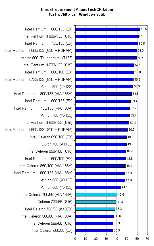
The situation is pretty much the same at 1024 x 768 x 32 under UT. Here the UT engine has some inherent limitations which keep the frame rates so low when compared to Quake III Arena for example.
Notice a trend here? The performance standings aren't changing much at all. The Celeron 700 is no match for the Duron which is easily beating the equivalently clocked Celeron by about 15 fps.
The Celeron is clearly not a high end contender, nor was it ever intended to be one. But it is interesting to note that the Duron, another CPU not intended to be a high end contender is actually performing quite well here.
Gaming under Windows 2000 remains relatively unchanged from Windows 98SE, the performance standings are virtually identical.
At the higher resolution the memory bandwidth of our test bed's GeForce 2 GTS becomes a limitation thus resulting in the similar performance across the board for most of the CPUs. Once again the Celerons are pulling up the end of the performance chart, the Duron clearly has the advantage and unless Intel severly drops the price of the Celeron line they are going to have some pretty hefty competition on their hands.
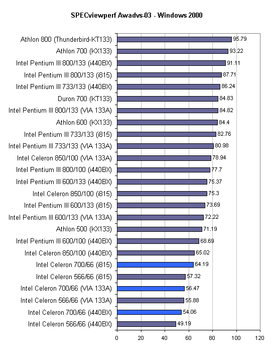
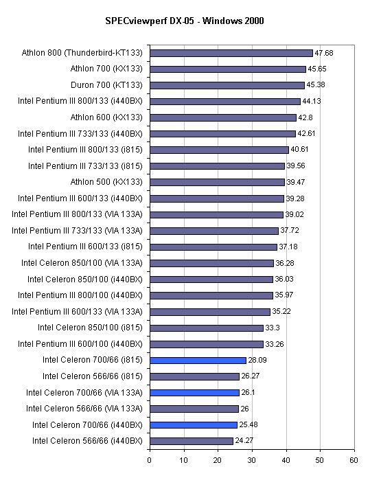
Under SPECviewperf the platform we ran the Celerons on seemed to make a much bigger difference than before. While the VIA 133A used to be able to edge out the i815, the Celeron 566 running on the i815 is even beating the 700MHz CPU running on the 133A.
If you take this one step further and realize that the KT133 chipset the Thunderbird is using is actually using the same memory controller as the 133A while the Thunderbird is still dominating the test you can begin to imagine how fast the Thunderbird/Duron would be if they had a platform with a better memory controller.
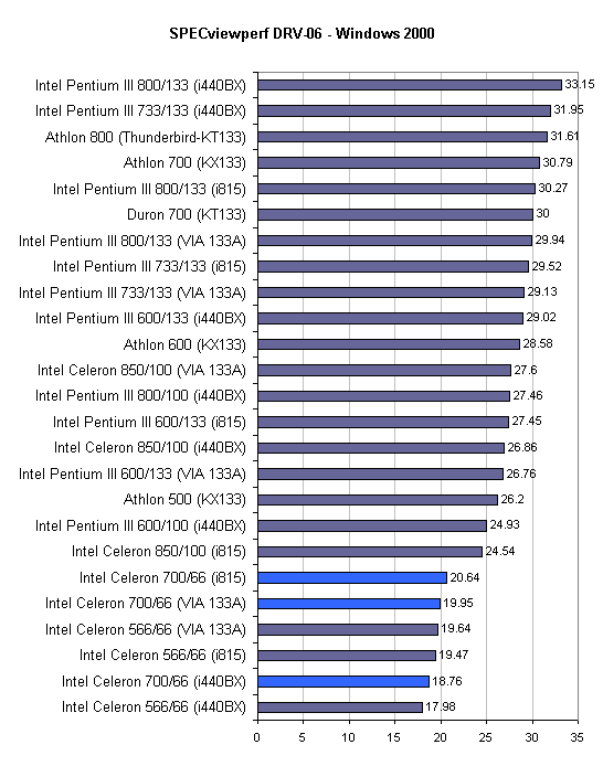
The Design Review benchmark is a bit more effected by CPU performance than memory performance (but not by a great amount) than the previous test. The standings still remain fairly similar, the Duron is a much better "value" processor for high end applications as we've proved with the past two SPECviewperf tests and as we will prove with the next three.
The situation is pretty similar under the Data Explorer viewset.
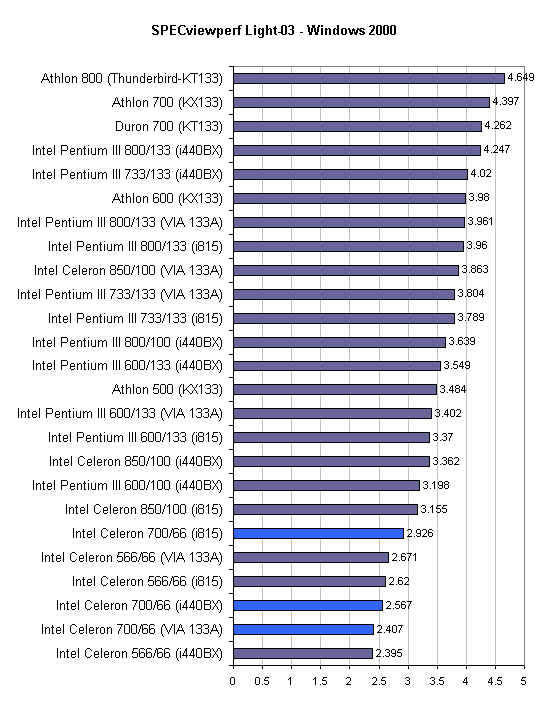
Under the Lightscape test the Duron 700 completely dominated as we discovered not too long ago. And if the overclocked Celeron running at 850/100MHz wasn't capable of coming close to the Duron 700 there's no way that the Celeron 700 with a 66MHz FSB/memory bus could touch AMD's new baby.
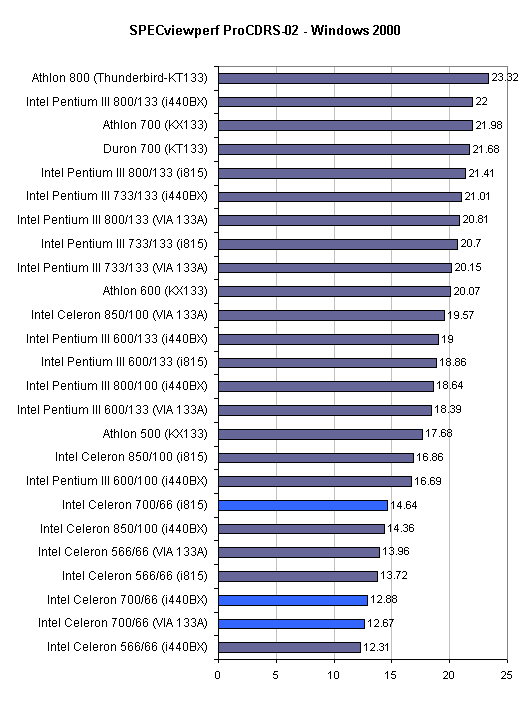
Nothing really new here, because of the i815's ability to run the memory bus at 100MHz the Celeron 700/66 on the i815 it actually is about the same speed as an 850/100 on a BX board. The ProCDRS-02 viewset under SPECviewperf is more memory bandwidth dependent than CPU dependent which is obvious by the lack of a performance improvement provided by the Celeron 850/100 on a BX board over the Celeron 700/66 (with a 100 MHz memory interface) on an i815 setup.
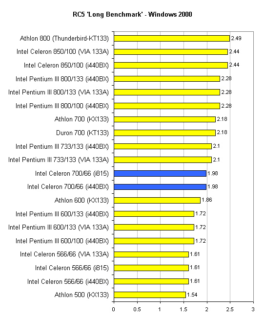
As we promised before we're continuing the inclusion of the RC5 benchmark in our CPU reviews. . For those that don't know, the RC5 is a form of encryption. Distributed.net is holding a challenge to crack the RC5 encryption to show that it is weak and encourage the implementation of stronger security. Click here to learn more about the Distributed.net challenge and join Team AnandTech for the opportunity to win $1000.
Once again what really matters here is CPU speed and not the platform or memory speed which is why the BX and i815 are bringing the exact same performance to the table.
Conclusion
The Celeron 700 is another step in the Celeron line and it is another reminder to Intel that the Celeron needs a 100MHz FSB and 100MHz memory bus in order to compete with the Duron. Even then, we're not entirely sure if the 100MHz FSB is enough to make the Celeron compete with the Duron which is clearly dominating the value market right about now.
If you care about performance at all you'll want to stay away from the Celeron 700, you're better off trying to overclock a lower clocked Celeron if you must go down that path otherwise the Duron is clearly the solution for you. With overclocking reports already emerging that the Duron 700 can hit the 900 - 950MHz pretty easily, so long as you're using the right motherboard, there shouldn't be a reason for you to go with anything other than AMD's new value performance leader.


