ECS L7VTA (KT400): 1st with 333MHz FSB Support
by Evan Lieb on September 24, 2002 12:00 PM EST- Posted in
- Motherboards
BIOS Setup and Overclocking Features
The ECS L7VTA utilizes the Award BIOS setup, which is a very common motherboard BIOS these days. This particular BIOS is not unlike all the other Award BIOS on the market, but there are still some nice features worth mentioning.
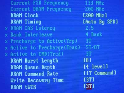
For example, we were happy that the Advanced Chipset Features section included lots of DRAM tweaking options. We were allowed to adjust CAS Latency, memory timing mode, bank interleave, Precharge to Active, Active to Precharge, Active to CMD, Burst Length, Queue Depth, and Command Rate to very aggressive settings if necessary.
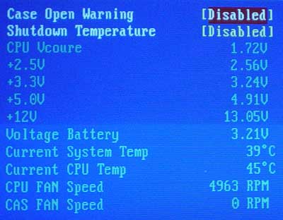
The PC Health section was also fairly detailed. We were able to view PSU readings, System Temperature readings, and several CPU readings (core temp, fan RPM, Vcore, etc.). There was also an option for shutting down the system if the CPU were to exceed a certain temperature.
A bit of a negative aspect of the L7VTA is the lack of virtually any memory or FSB overclocking options. There are no CPU:DRAM ratios available via the BIOS. The only options you have for memory speeds are DDR266, DDR333, and DDR400.
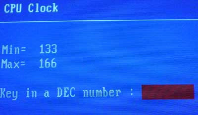
Our FSB overclocking results didn't go too well either. We were only able to hit 141MHz using a Foxconn heatsink (AS III thermal compound) and stock voltages before the system became increasingly unreliable. In addition, there's no AGP/PCI lock option in the BIOS, which is definitely a negative aspect of this motherboard if you plan on performing any type of decent overclocking.
Another negative aspect of this BIOS was a lack of any voltage options. There are no AGP, Vcore, or VDIMM voltage adjustments available via the BIOS.


0 Comments
View All Comments