The Haswell Review: Intel Core i7-4770K & i5-4670K Tested
by Anand Lal Shimpi on June 1, 2013 10:00 AM EST
This is a very volatile time for Intel. In an ARM-less vacuum, Intel’s Haswell architecture would likely be the most amazing thing to happen to the tech industry in years. In mobile Haswell is slated to bring about the single largest improvement in battery life in Intel history. In graphics, Haswell completely redefines the expectations for processor graphics. There are even some versions that come with an on-package 128MB L4 cache. And on the desktop, Haswell is the epitome of polish and evolution of the Core microprocessor architecture. Everything is better, faster and more efficient.
There’s very little to complain about with Haswell. Sure, the days of insane overclocks without touching voltage knobs are long gone. With any mobile-first, power optimized architecture, any excess frequency at default voltages is viewed as wasted power. So Haswell won’t overclock any better than Ivy Bridge, at least without exotic cooling.
You could also complain that, for a tock, the CPU performance gains aren’t large enough. Intel promised 5 - 15% gains over Ivy Bridge at the same frequencies, and most of my tests agree with that. It’s still forward progress, without substantial increases in power consumption, but it’s not revolutionary. We compare the rest of the industry to Intel’s excellent single threaded performance and generally come away disappointed. The downside to being on the top is that virtually all improvements appear incremental.
The fact of the matter is that the most exciting implementations of Haswell exist outside of the desktop parts. Big gains in battery life, power consumption and even a broadening of the types of form factors the Core family of processors will fit into all apply elsewhere. Over the coming weeks and months we’ll be seeing lots of that, but today, at least in this article, the focus is on the desktop.


Haswell CPU Architecture Recap
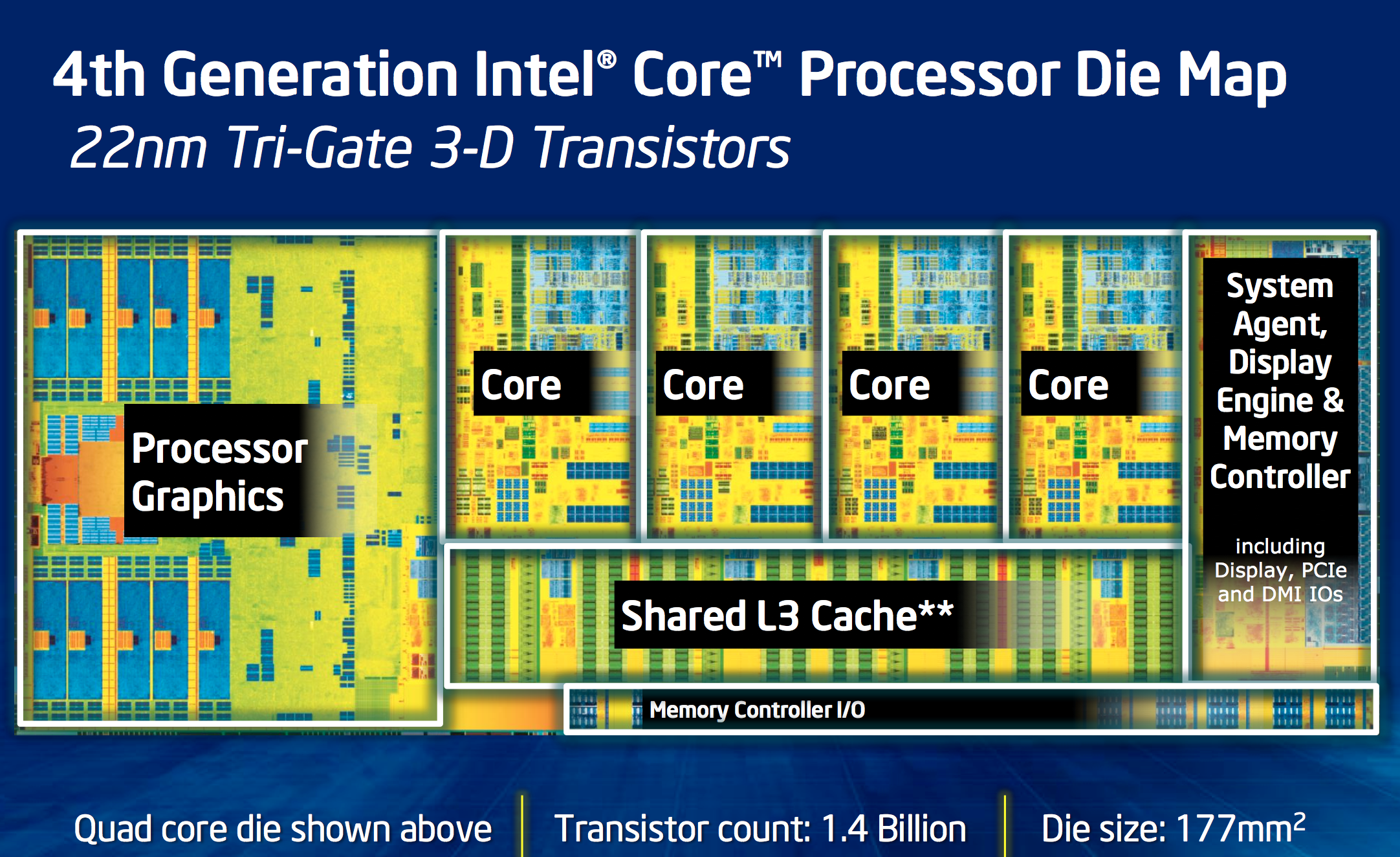
Haswell is Intel’s second 22nm microprocessor architecture, a tock in Intel’s nomenclature. I went through a deep dive on Haswell’s Architecture late last year after IDF, but I’ll offer a brief summary here.
At the front end of the pipeline, Haswell improved branch prediction. It’s the execution engine where Intel spent most of its time however. Intel significantly increased the sizes of buffers and datastructures within the CPU core. The out-of-order window grew, to feed an even more parallel set of execution resources.
Intel added two new execution ports (8 vs 6), a first since the introduction of the Core microarchitecture back in 2006.
On the ISA side, Intel added support for AVX2, which includes an FMA operation that considerably increases FP throughput of the machine. With a doubling of peak FP throughput, Intel doubled L1 cache bandwidth to feed the beast. Intel also added support for transactional memory instructions (TSX) on some Haswell SKUs.
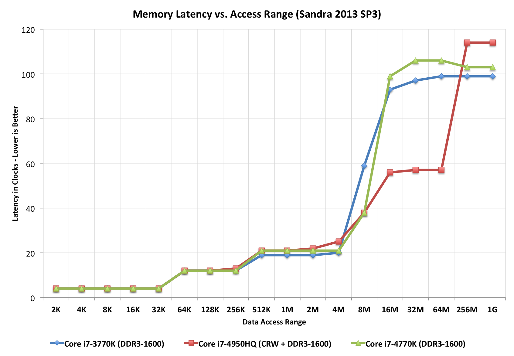
The L3 cache is now back on its own power/frequency plane, although most of the time it seems to run in lockstep with the CPU cores. There appears to be a 2 - 3 cycle access penalty as a result of decoupling the L3 cache.


210 Comments
View All Comments
chizow - Saturday, June 1, 2013 - link
The other big problem with the CPU space besides the problems with power consumption and frequency, is the fact Intel has stopped using it's extra transistor budget from a new process node on the actual CPU portion of the die long ago. Most of the increased transistor budget afforded by a new process goes right to the GPU. We will probably not see a stop to this for some time until Intel reaches discrete performance equivalency.Jaybus - Monday, June 3, 2013 - link
Well, I don't know. Cache sizes have increased dramatically.chizow - Monday, June 3, 2013 - link
Not per core, these parts are still 4C 8MB, same as my Nehalem-based i7. Some of the SB-E boards have more cache per core, 4C 10MB on the 3820, 6C 15MB on the 3960/3970, but the extra bit results in a negligible difference over the 2MB per core on the 3930K.Boissez - Sunday, June 2, 2013 - link
I think you've misunderstood me.I'm merely pointing out that, in the past 2½ years we've barely seen any performance improvements in the 250-300$ market from Intel. And that is in stark contrast to the developments in mobileland. They too, are bound by the constraints you mention.
And please, stop the pompous know-it-all attitude. For the record, power consumption actually rises *linearly* with clock speed and *quadratically* with voltage. If your understanding of Joule's law and Ohm's law where better developed you would know.
klmccaughey - Monday, June 3, 2013 - link
Exactly. And it won't change until we see optical/biological chips or some other such future-tech breakthrough. As it is the electrons are starting to behave in light/waveform fashion at higher frequencies if I remember correctly from my semiconductor classes (of some years ago I might add).Jaybus - Monday, June 3, 2013 - link
Yes, but we will first see hybrid approaches. Intel, IBM, and others have been working on them and are getting close. Sure, optical interconnects have been available for some time, but not as an integrated on-chip feature which is now being called "silicon photonics". Many of the components are already there; micro-scale lenses, waveguides, and other optical components, avalanche photodiode detectors able to detect a very tiny photon flux, etc. All of those can be crafted with existing CMOS processes. The missing link is a cheaply made micro-scale laser.Think about it. An on-chip optical transceiver at THz frequencies allows optical chip-to-chip data transfer at on-chip electronic bus speeds, or faster. There is no need for L2 or L3 cache. Multiple small dies can be linked together to form a larger virtual die, increasing productivity and reducing cost. What if you could replace a 256 trace memory bus on a GPU with a single optical signal? There are huge implications both for performance and power use, even long before there are photonic transistors. Don't know about biological, but optical integration could make a difference in the not-so-far-off future.
tipoo - Saturday, June 1, 2013 - link
It's easier to move upwards from where ARM chips started a few years back. A bit like a developing economy showing growth numbers you would never see in a developed one.Genx87 - Saturday, June 1, 2013 - link
Interesting review. But finding it hard to justify replacing my i2500K. I guess next summer on the next iteration?kyuu - Saturday, June 1, 2013 - link
Agreed, especially considering Haswell seems to be an even poorer overclocker than Ivy Bridge. My i5-2500k @ 4.6GHz will be just fine for some time to come, it seems.klmccaughey - Monday, June 3, 2013 - link
Me too. I have a 2500k @ 4.3Ghz @ 1.28v and I am starting to wonder if even the next tick/tock will tempt me to upgrade.Maybe if they start doing a K chip with no onboard GPU and use the extra silicon for extra cores? Even then the cores aren't currently used well @ 4. But maybe concurrency adoption will increase as time goes by.