Intel's Haswell Architecture Analyzed: Building a New PC and a New Intel
by Anand Lal Shimpi on October 5, 2012 2:45 AM ESTOther Power Savings
Haswell's power savings come from three sources, all of which are equally important. We already went over the most unique: Intel's focus on reducing total platform power consumption by paying attention to everything else on the motherboard (third party controllers, voltage regulation, etc...). The other two sources of power savings are more traditional, but still very significant.
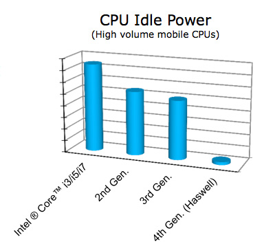
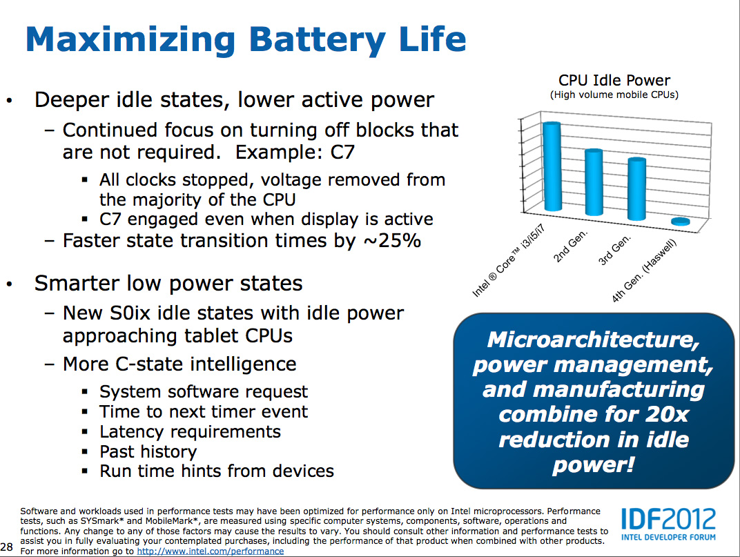
At the micro-architecture level Intel added more power gating and low power modes to Haswell. The additional power gating gives the power control unit (PCU) more fine grained control over shutting off parts of the core that aren't used. Intel published a relatively meaningless graph showing idle power for standard voltage mobile Haswell compared to the previous three generations of Core processors.
Haswell can also transition between power states approximately 25% faster than Ivy Bridge, which lets the PCU be a bit more aggressive in which power state it selects since the penalty of coming out of it is appreciably lower. It's important to put the timing of all of this in perspective. Putting the CPU cores to sleep and removing voltage/power from them even for a matter of milliseconds adds up to the sort of savings necessary to really enable the sort of always-on, always-connected behavior Haswell based systems are expected to deliver.
Intel has also done a lot of work at the process level to bring Haswell's power consumption down. As a tock, Haswell is the second micro-architecture to use Intel's new 22nm tri-gate transistors. The learnings from Ivy Bridge are thus all poured into Haswell. Intel wasn't too specific on what it did on the manufacturing side to help drive power down in Haswell other than to say that a non-insignificant amount of work came from the fabs.
The Fourth Haswell
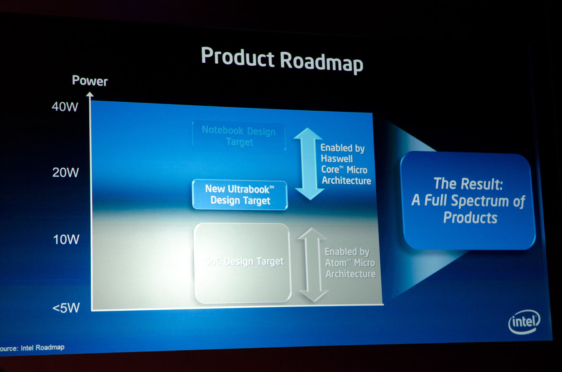
At Computex Intel's Mooly Eden showed off this slide that positioned Haswell as a 15-20W part, while Atom based SoCs would scale up to 10W and perhaps beyond:
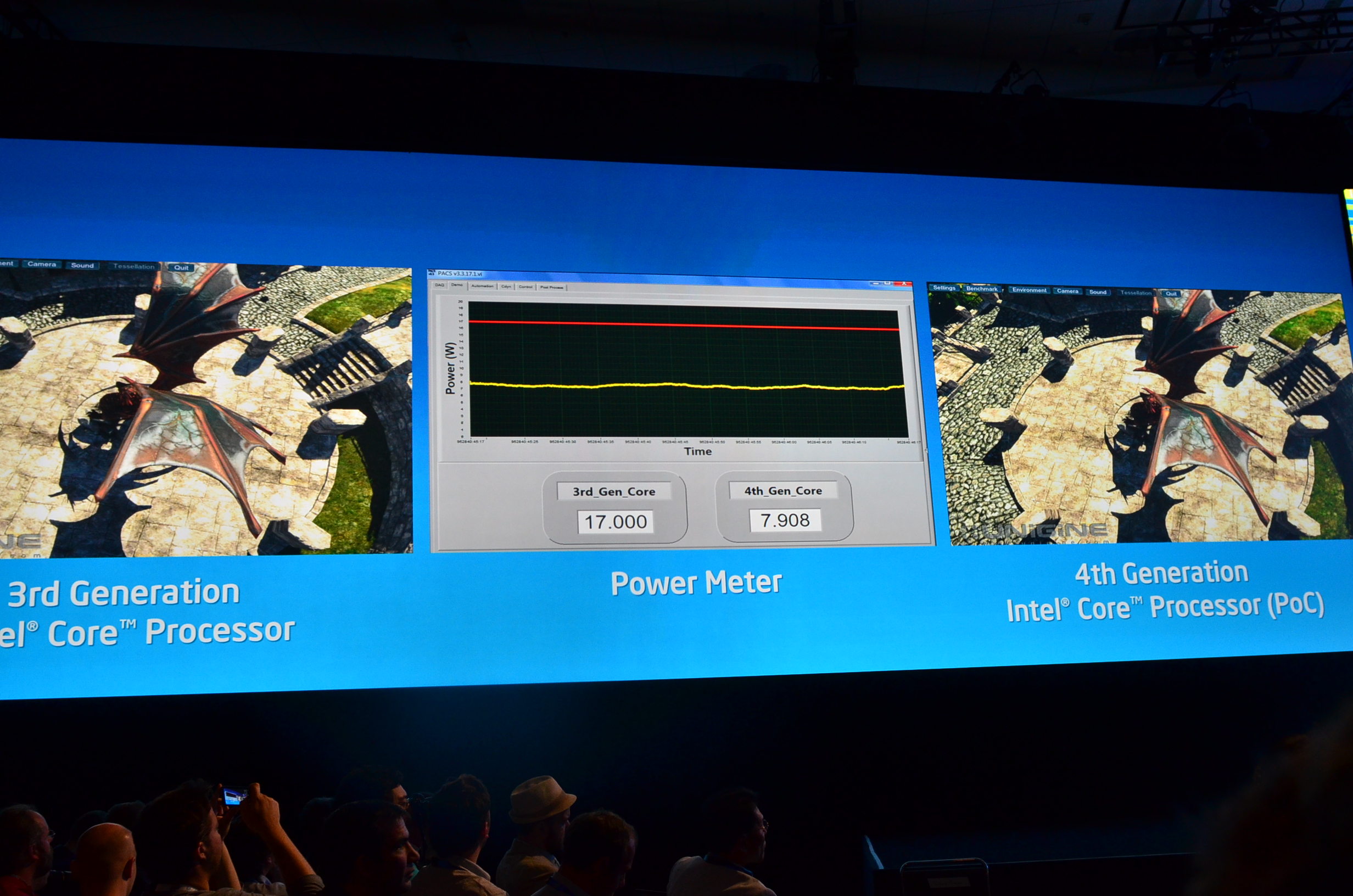
Just before this year's IDF Intel claimed that Haswell ULT would start at 10W, down from 17W in Sandy/Ivy Bridge. Finally, at IDF Intel showed a demo of Haswell running the Unigen Heaven benchmark at under 8W:
The chain of events tells us two things: 1) Intel likes to play its cards close to its chest, and 2) the sub-10W space won't be serviced by Atom exclusively.
Intel said Haswell can scale below 10W, but it didn't provide a lower bound. It's too much to assume Haswell would go into a phone, but once you get to the 8W point and look south you open yourself up to fitting into things the size of a third generation iPad. Move to 14nm, 10nm and beyond then it becomes more feasible that you could fit this class of architecture into something even more portable.
Intel is being very tight lipped about the fourth client Haswell (remember the first three were desktop, mobile and ultra-low-volt/Ultrabook) but it's clear that it has real aspirations to use it in a space traditionally reserved for ARM or Atom SoCs.
One of the first things I ever heard about Haswell was that it was Intel's solution to the ARM problem. I don't believe a 10W notebook is going to do anything to the ARM problem, but a sub-8W Haswell in an iPad 3 form factor could be very compelling. Haswell won't be fanless, but Broadwell (14nm) could be. And that could be a real solution to the ARM problem, at least outside of a phone.
As I said before, I don't see Haswell making it into a phone but that's not to say a future derivative on a lower power process wouldn't.


245 Comments
View All Comments
Da W - Friday, October 5, 2012 - link
AMD spend 1/10th of Intel in R&D. There are things they just cant do, i suspect pursuing higher x86 single trend performance is one of them.StevoLincolnite - Saturday, October 6, 2012 - link
However, allot of the R&D Intel spends is on lithography type technologies, AMD doesn't have to spend Billions on such things anymore.Besides, a simple way for AMD to beat Intel when Intel is a node ahead is to throw more transistors at the problem which they have succeeded very well at doing in the past.
Mind you, that comes at the cost of power and die size, however with stuff like clock mesh it can negate some of that.
Kevin G - Friday, October 5, 2012 - link
Being four steps behind ARM isn't necessarily a bad thing unless you're trying to leap frog them. AMD appears to be content with letting Intel spearhead the effort to get into the ultramobile market. With Intel two steps behind of ARM and they couldn't leap frog over ARM, there is little chance that AMD would be able to do the same. It isn't just knowing what battles to fight but also when to fight them.abufrejoval - Friday, October 5, 2012 - link
It was only when I was reading Jana Rutkowska's notes on the current UI limitations within Qubes, that I finally understood (I believe!) the message which AMD has been pushing for quite a few years now: GPU compute will truly be an integral part of their future APUs in one or two generations, becoming almost an augmented instruction set instead of just a SoC.Currently all Qubes "user" applications, that is everything except the Dom0, can't use the GPU to render their graphics: It's basically software rendering into an off-screen composition buffer and then GPU assisted composition of these software buffers onto the visible screen (this time with all the wobble and transition effects we've all come to expect and love ;-)
That's because although the GPU is on the same die even on the newest Trinity class APUs, it's still logically very separate, sharing only some stuff but bypassing, I believe, the ordinary page tables (not the IOMMU ones) and the snooping logic for caches. So even if GPU and CPU sit on the same die and use the same phyiscal DRAM bus, doing GPU compute implies using a dedicated part of that RAM in a way, which doesn't mesh seamlessly with CPU compute.
But the roadmap seems to imply, that this limitation will go away, which would allow e.g. Qubes to use GPU assisted rendering anywhere in user space memory and thus also into a per DomU virtual framebuffer composed of quite ordinary paged virtual memory, which could then be assembled by the Dom0 for the visible screen or for video encoding and streaming to a remote display device e.g. for cloud gaming.
This easy feeding of GPU "results" into another software layer is currently either impossible or requires major fiddling with device drivers so it's limited to the GPU vendors and bilateral deals such as nVidia and Splashtop. Once the GPU becomes more of an augmented instruction set, allowing OpenCL or even hardware primitives on ordinary user space paged virtual memory, this becomes as natural as running virtual machines with hardware virtualization.
And at that point even the new 256bit FMA may look pretty lame compared to what hundreds of APU EUs could do. That to me explains rather well, why AMD isn't spending more transistors on a vastly improved CPU only x86 ISA: It truly belives it's a dead end for both personal and scientific workloads.
It's a very daring bet and I very much admire them for having the vision and the balls to tie the company's survival to it. Over the last 40 years Intel seems to have failed with most of its visions (80432, i860, Itanium), but excelled on evolving x86. AMD, however, seems better on vision and noticably 2nd rate on execution.
APUs are potentially quite dangerous both to nVidia and to Intel, because both can't easily duplicate them: The AMD/Intel cross licensing deal IMHO won't cover the GPU portion. Unless nVidia and Intel join, which would only happen if either of the two is in truly dire straights.
But quite a few things need to fall in place over the next couple of years and AMD needs to survive them for that potential to develop. And it looks like all ther other players aren't standing still.
Events like Apple potentially using Samsung augmented cash billions to turn TMSC into a private provider of 1x nm ARM SoCs are sending shock waves into the market, which may force "strange" alliances.
These days when even trival things like "swipe to unlock" can be patented and used to bloodlet competitors I'm surprised to see IBM and Intel use things like transactional memory, which saw silocon first with Sun's Rock, I believe, or Intel turning to eDRAM for caches and frame buffers, which IBM's been implementing first on the p-Series.
That leads me to an open question on the commercial workloads, which is almost the only domain, where I have difficulties seeing the immediate benefit of APUs, at least after Oracle's grab on Java and their expressed intent to make commercial workloads a SPARC exclusive (please see Larry's opening remarks on Openworld 2012): How can AMD make APUs the better Java and database engines? How can they make search, big data, map reduced or JavaScript run better on APUs?
I can only guess that having managed CPU+GPU AMD would be in a better position to add xPU for all of the above.
ltcommanderdata - Friday, October 5, 2012 - link
A great, detailed description of Haswell's architecture. I do have some questions though.You mentioned that Intel will be including up to 1 redundant EU in the GPU array. Does that mean only GT3 will have the 1 redundant EU (41 total, 40 usable) with GT2 having no redundancy? Or is it 1 redundant EU per sub-slice, so GT2 will have 1 and GT3 will have 2?
Will the embedded DRAM be implemented PoP like in SoC? When you say we'll see a version of Haswell with embedded DRAM do will all GT3 have embedded DRAM or will only some GT3 have embedded DRAM (kind of a GT4)?
Given the long timescales of CPU design, there would be overlap between the Haifa team working on Sandy Bridge/Ivy Bridge (particularly Ivy Bridge) and the Hillsboro team working on Haswell. I was wondering if you knew how much opportunity there is for learning between consecutive designs in terms of magnitude of changes possible and timescales before things are pretty much fixed? I'm in no position to judge, but I was also wondering based on your knowledge of the architectures and/or interactions with members of the design teams if you sense any distinct difference in design philosophies between the Haifa and Hillsboro teams. Afterall, the Haifa team's background was in power-efficient, mobile-oriented designs whereas Hillsboro was high-performance, desktop/server oriented. You mentioned in the article that Haswell goes back to Nehalem's 3 clock domains due to lessons learned from Sandy Bridge/Ivy Bridge. While I don't doubt that's the primary reason, I wonder if design philosophy played a role too since Nehalem and Haswell are both Hillsboro designs and maybe they like 3 clock domains.
Anand Lal Shimpi - Friday, October 5, 2012 - link
Unfortunately that's all the info I have on redundancy in the GPU array. I think we'll have to wait until we're closer to launch to know more. The same goes for the nature of the on-package memory.I wondered the same thing about the correlation between design teams and decisions in Nehalem/Haswell, I refrained from speculating on it in the article because I didn't necessarily see any reason to doing so, but I definitely noticed the same correlation. It could just be a coincidence though. Nothing else beyond the L3 cache frequency really stood out to me as being an obvious common thread between Nehalem and Haswell though.
Take care,
Anand
ltcommanderdata - Friday, October 5, 2012 - link
Thanks again for your insights.tipoo - Friday, October 5, 2012 - link
Speaking of the EUs, is the GT3 part twice as fast as the HD4000 with or without the eDRAM cache? The article seems to imply with, but then what is the performance without it if they've doubled the EUs? Doesn't it seem more likely they doubled performance without the cache, and the cache doubles it beyond that?telephone - Friday, October 5, 2012 - link
Anand, thanks for the insights. We all enjoyed it very much and look forward to getting the real thing into your labs.To clarify some questions:
As for the design team philosophy, the Hillsboro design team continually tries to outdo the Haifa design team and vice versa. Both teams have access to the other teams' design collateral, as we co-own the tick-tock model.
Next, the reasons for the "3" clock domains are too complicated (and confidential) to go into. Since designing for "2" clock domains is much simpler, the reason is not that we enjoy pain and misery. Suffice to say, that you are missing a very big piece of the puzzle and accurate conclusions as to why this was done cannot be drawn from the information you have. And the number of clock domains is in quotes because those are not accurate anyhow.
Sincerely,
Someone from the Hillsboro Design Team
Stahn Aileron - Friday, October 5, 2012 - link
I'm curious as to whether Intel has enough interest to drive the Atom design low enough to hit ARM power level (like Medfield) and integrate an Atom core into a Core CPU design. nVidia introduced a heterogeneous CPU in their Tegra 3 SoC. (Two different ARM core types in the CPU block). From all the stuff I've seen about Intel over the past half decade, I'm pretty sure they have the resources to pull that off. They have top-notch designers and engineers with the basic tech and designs need to start R&D on that, I think.On the other hand, if they really are trying to force a Core design in Atom territory... Well, hell ya ^_~ Still, I can't really see Core hitting the sub-1W power levels they've been able to do with Atom (Medfield). I figure using an Atom core for basic S0ix functions would be a little more power efficient than using a Core design, but I'm no silicon engineer. Intel would know about that far better than me.