Intel's Haswell Architecture Analyzed: Building a New PC and a New Intel
by Anand Lal Shimpi on October 5, 2012 2:45 AM ESTThe Haswell Front End
Conroe was a very wide machine. It brought us the first 4-wide front end of any x86 micro-architecture, meaning it could fetch and decode up to 4 instructions in parallel. We've seen improvements to the front end since Conroe, but the overall machine width hasn't changed - even with Haswell.
Haswell leaves the overall pipeline untouched. It's still the same 14 - 19 stage pipeline that we saw with Sandy Bridge depending on whether or not the instruction is found in the uop cache (which happens around 80% of the time). L1/L2 cache latencies are unchanged as well. Since Nehalem, Intel's Core micro-architectures have supported execution of two instruction threads per core to improve execution hardware utilization. Haswell also supports 2-way SMT/Hyper Threading.
The front end remains 4-wide, although Haswell features a better branch predictor and hardware prefetcher so we'll see better efficiency. Since the pipeline depth hasn't increased but overall branch prediction accuracy is up we'll see a positive impact on overall IPC (instructions executed per clock). Haswell is also more aggressive on the speculative memory access side.
The image below is a crude representation I put together of the Haswell front end compared to the two previous tocks. If you click the buttons below you'll toggle between Haswell, Sandy Bridge and Nehalem diagrams, with major changes highlighted.
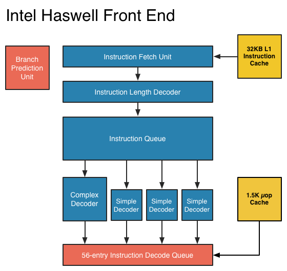
In short, there aren't many major, high-level changes to see here. Instructions are fetched at the top, sent through a bunch of steps before getting to the decoders where they're converted from macro-ops (x86 instructions) to an internally understood format known to Intel as micro-ops (or µops). The instruction fetcher can grab 4 - 5 x86 instructions at a time, and the decoders can output up to 4 micro-ops per clock.
Sandy Bridge introduced the 1.5K µop cache that caches decoded micro-ops. When future instruction fetch requests are made, if the instructions are contained within the µop cache everything north of the cache is powered down and the instructions are serviced from the µop cache. The decode stages are very power hungry so being able to skip them is a boon to power efficiency. There are also performance benefits as well. A hit in the µop cache reduces the effective integer pipeline to 14 stages, the same length as it was in Conroe in 2006. Haswell retains all of these benefits. Even the µop cache size remains unchanged at 1.5K micro-ops (approximately 6KB in size).
Although it's noted above as a new/changed block, the updated instruction decode queue (aka allocation queue) was actually one of the changes made to improve single threaded performance in Ivy Bridge.
The instruction decode queue (where instructions go after they've been decoded) is no longer statically partitioned between the two threads that each core can service.
The big changes in Haswell are at the back end of the pipeline, in the execution engine.


245 Comments
View All Comments
random2 - Saturday, October 6, 2012 - link
"The race to the bottom that we've seen in the LCD space made it unlikely that any of the panel vendors would be jumping at the opportunity to make their products more expensive."It's unfortunate, because of what might have been had the manufacturers, of which there are only three main ones, if I recall, had the foresight to market to customers that weren't just looking to buy the lowest priced panel on display at Best Buy. Had they the initiative to have started years ago, there would be some pretty fantastic panels available today for much more reasonable prices than seen for the 27 and 30 inch 2560X1600 panels today.
Klugfan - Saturday, October 6, 2012 - link
This doesn't really belong in the Haswell article, but I would love to know more about the physics and constraints of TDP. Like, hit me with a chart of TDP impact for a variety of important parts in phones, tablets, laptops, and desktops. Show me a chart of TDP budgets and mitigation strategies. Explain to me roughly how physics forces those things to relate. Please.Seems important and it's easy to understand the comparison from Ivy Bridge to Haswell but that doesn't feel like the big picture.
havoti97 - Saturday, October 6, 2012 - link
I read the 1st page then got bored. Writing style is overly wordy... am I the only the feeling this way?xeizo - Saturday, October 6, 2012 - link
It's an article, not a twitter feed! Some of us like to get the whole picture not just the flashy stuff ....watersb - Saturday, October 6, 2012 - link
Phenomenal feature, Anand! This is why I check your site each day. Thanks very much!bill4 - Saturday, October 6, 2012 - link
like atom, you're stuck in no mans land. way too high for tablets and phones, but in desktops and laptop, who cares if the amd solution uses 30 watts instead of 8? that difference isn't enough to matter when you take the whole platform into account, especially at lower price points where battery life wont be fantastic anyway. on the dsktop it's completely pointless.JlHADJOE - Sunday, October 7, 2012 - link
On a laptop using 30 watts instead of 8 will more than triple your battery life, especially at lower price points/smaller form factors where manufacturers gimp the battery.How's about browsing for 9 hours instead of 3? Or 27 hours instead of 9? I'd jump on it in a heartbeat.
1008anan - Saturday, October 6, 2012 - link
Haswell will sport 32 single precision or 16 double precision flops per cycle per core for its desktop and high tdp mobile skews [at least 30 watt and up].Can anyone speculate on how many single precision and double precision flops per cycle per core Haswell will execute for its low TDP skews? For example the less than 10 watt skews? the 15 watt skews?
I would also be interested in learning speculation about how many execution units (or shader cores if you prefer standard nomenclature) the low TDP Haswell products will have.
1008anan - Saturday, October 6, 2012 - link
Haswell will be able to execute 16 double precision or 32 single precision flops per clock per core for desktop and high TDP mobile skews [at least 30 watts and up].Can anyone speculate on how many flops per cycle per core the sub 10 watt and 15 watt Haswell skews will execute? Similarly I would be interested in hearing speculation about how many graphic execution units (shader cores) the sub 10 watt and 15 watt Haswell products will come with. Any speculation on graphics clock speed?
Is it possible that the high end tock 22 nm Xeon server parts could have 32 double precision or 64 single precision flops per clock per core?
Laststop311 - Saturday, October 6, 2012 - link
Best explanation of haswell I've read to date. Good Job Anand.