Intel's Haswell Architecture Analyzed: Building a New PC and a New Intel
by Anand Lal Shimpi on October 5, 2012 2:45 AM ESTHaswell's GPU
Although Intel provided a good amount of detail on the CPU enhancements to Haswell, the graphics discussion at IDF was fairly limited. That being said, there's still some to talk about here.
Haswell builds on the same fundamental GPU architecture we saw in Ivy Bridge. We won't see a dramatic redesign/re-plumbing of the graphics hardware until Broadwell in 2014 (that one is going to be a big one).
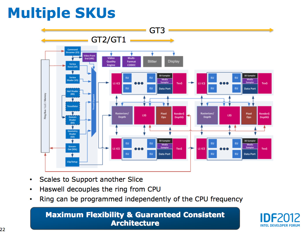
Haswell's GPU will be available in three physical configurations: GT1, GT2 and GT3. Although Intel mentioned that the Haswell GT3 config would have twice the shader count of Haswell GT2, it was careful not to disclose the total number of EUs in any of the versions. Based on the information we have at this point, GT3 should be a 40 EU configuration while GT2 should feature 20 EUs. Intel will also be including up to one redundant EU to deal with the case where there's a defect in an EU in the array. This isn't an uncommon practice, but it does indicate just how much of the die will be dedicated to graphics in Haswell. The larger of an area the GPU covers, the greater the likelihood that you'll see unrecoverable defects in the GPU. Redundancy at the EU level is one way of mitigating that problem.
Haswell's processor graphics extends API support to DirectX 11.1, OpenCL 1.2 and OpenGL 4.0.
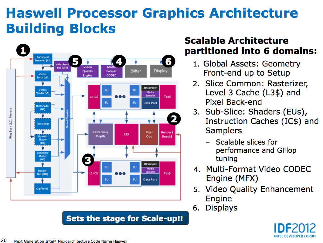
At the front of the graphics pipeline is a new resource streamer. The RS offloads some driver work that the CPU would normally handle and moves it to GPU hardware instead. Both AMD and NVIDIA have significant command processors so this doesn't appear to be an Intel advantage although the devil is in the (unshared) details. The point from Intel's perspective is that any amount of processing it can shift away from general purpose CPU hardware and onto the GPU can save power (CPU cores go to sleep while the RS/CS do their job).
Beyond the resource streamer, most of the fixed function graphics hardware sees a doubling of performance in Haswell.
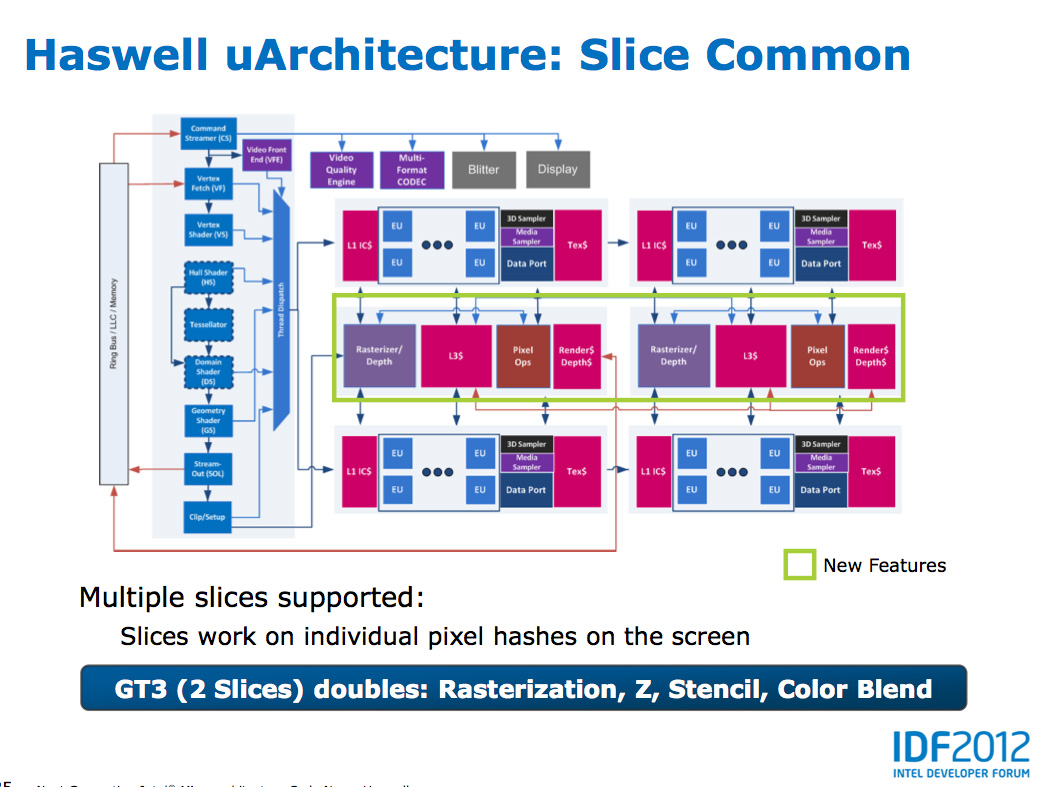
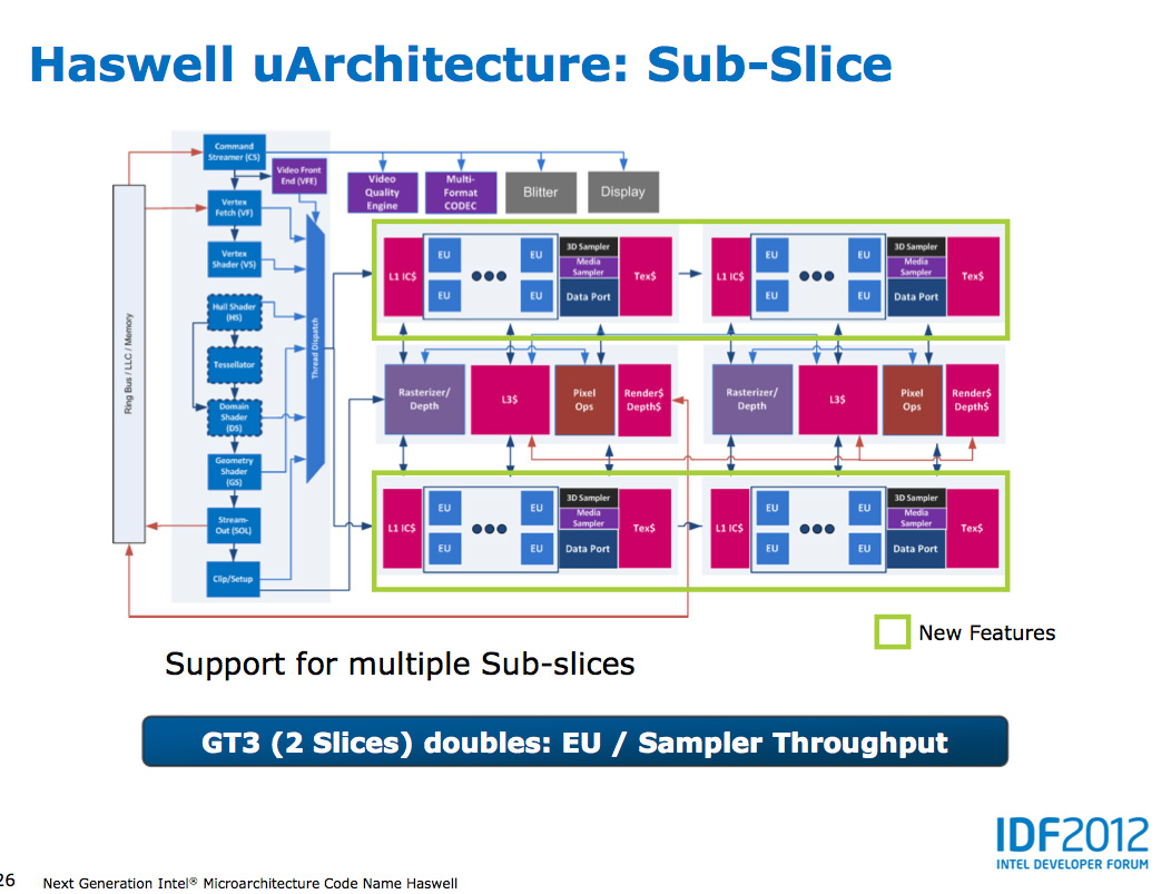
At the shader core level, Intel separates the GPU design into two sections: slice common and sub-slice. Slice common includes the rasterizer, pixel back end and GPU L3 cache. The sub-slice includes all of the EUs, instruction caches and EUs.
In Haswell GT1 and GT2 there's a single slice common, while GT3 sees a doubling of slice common. GT3 similarly has two sub-slices, although once again Intel isn't talking specifics about EU counts or clock speeds between GT1/2/3.
The final bit of detail Intel gave out about Haswell's GPU is the texture sampler sees up to a 4x improvement in throughput over Ivy Bridge in some modes.
Now to the things that Intel didn't let loose at IDF. Although originally an option for Ivy Bridge (but higher ups at Intel killed plans for it) was a GT3 part with some form of embedded DRAM. Rumor has it that Apple was the only customer who really demanded it at the time, and Intel wasn't willing to build a SKU just for Apple.
Haswell will do what Ivy Bridge didn't. You'll see a version of Haswell with up to 128MB of embedded DRAM, with a lot of bandwidth available between it and the core. Both the CPU and GPU will be able to access this embedded DRAM, although there are obvious implications for graphics.
Overall performance gains should be about 2x for GT3 (presumably with eDRAM) over HD 4000 in a high TDP part. In Ultrabooks those gains will be limited to around 30% max given the strict power limits.
As for why Intel isn't talking about embedded DRAM on Haswell, your guess is as good as mine. The likely release timeframe for Haswell is close to June 2013, there's still tons of time between now and then. It looks like Intel still has a desire to remain quiet on some fronts.


245 Comments
View All Comments
Kevin G - Saturday, October 6, 2012 - link
Losing just the MacBook AIr isn't going to hurt Intel much as a whole but it is doubtful that Apple would just move that product line to ARM. The rest of the line up would likely follow. The results by the numbers would hurt Intel but nothing to doom the company. Intel does have the rest of the PC industry to fall back upon... except the PC market is shrinking.Apple is one of Intel's best gateway into the ultra mobile market. Apple has made indications that they want to merge iOS and OS X over the long term which would likely result in dropping either ARM or x86 hardware to simplify the line up.
WinRT is also a threat to Intel and
Kevin G - Saturday, October 6, 2012 - link
(Hrm... got cut off there)WinRT is also a threat to Intel but WinRT has next to zero market share. The threat here is any success it obtains. Apple on the other hand controls ~75% of the tablet market last I checked.
Andriod is a bit neutral to Intel as manufacturers can transition between ARM and x86 versions with relative ease. Intel will just have to offer competitive hardware at competitive prices here. The sub 10W Haswell parts are going to be competitive but price is a great unknown. The ARM SoC's are far cheaper than what Intel has traditionally been comfortable with. So even if Intel were to acquire all of the Android tablet market, it would be a minority at this time and over the short term (even in the best case scenario, it'd take time for Android based tablets to surpass the iPad in terms of market share).
So ultimately it would be best for Intel to snag Apple's support due to their dominant market share in the tablet space and influential position in the smart phone space.
andrewaggb - Friday, October 5, 2012 - link
Agree with others. Best Anandtech article I've read in a long time.Most articles lack the detail and insights that this one has.
mrdude - Friday, October 5, 2012 - link
Great article. Great depth, great info and very thorough. Hats off :)But I couldn't shake the feeling that I was missing perhaps the most important bit of information: price.
Obviously, Intel isn't going to give that away 9 months away from the presumed launch date -- though in typical fashion we'll see it leaked early. It still is the biggest question regarding Haswell's, and in turn Intel's, success against ARM.
I think most consumers are already at that good enough stage, where your Tegra 3 or Snapdragon S4 can fulfill all of their computing needs on a tablet or a phone. The biggest drawback for productivity purposes isn't necessarily the "lack of CPU performance" but rather the lack of a proper keyboard/mouse, gaming, along with a rare application or two that's still locked to x86 (Office rings a bell, though not for long). Or I should say, these were drawbacks. Not any longer.
So is Intel going to cut their margins and go for volume? Or are they just going to keep their massive margins and price themselves out of contention? Apple carries with itself a brand name that people want. It's become more than a gadget but a fashion accessory. People don't mind paying for Apple tax. I don't think I ever will, but at least I can notice the trend. The Intel brand doesn't carry with it the same cult following and neither does x86. Unless Intel is willing to compete with ARM on price, lowering the cost of their products below Apple's, I don't think think the substantial increases in efficiency and performance will matter all that much.
name99 - Friday, October 5, 2012 - link
"Sandy Bridge made ports 2 & 3 equal class citizens, with both capable of being used for load or store address calculation. In the past you could only do loads on port 2 and store addresses on port 3. Sandy Bridge's flexibility did a lot for load heavy code, which is quite common. Haswell's dedicated store address port should help in mixed workloads with lots of loads and stores."The rule of thumb numbers are, on "ordinary" integer type code:
1/6 instructions are branches
1/6 are writes
2/6 are reads
2/6 are ALU
This makes it more obvious why Intel moved as it did.
You want to sustain as close to 4ops/cycle as you can.
This means that your order of adding abilities should be exactly as Intel has done
- first two ALUs
- next two read/writes per cycle (ideal would be a mix of load/store) but Intel gave us that you can do a load+store per cycle
- next two loads per cycle
- next make sure the branches aren't throttled (because back-to-back branches are common, and you want branches resolved ASAP)
- next make the load-store system wide enough to sustain a MAC per cycle (two loads+store)
It's hard to see what is left to complain about at this level.
And of course we have better lock performance. So what's left?
What I think still have substantial room for improvement (correct me if I'm wrong) is
(a) TLB coverage
(b) TLB efficiency.
TLB coverage could be improved with a 2nd level TLB but (as far as I know) Intel doesn't go in for that, unlike POWER.
By TLB efficiency, I mean not needing to lose performance due to different address spaces. Unfortunately Intel seems screwed here. The POWER segment scheme (especially the 64-bit scheme) is REALLY powerful here in allowing multiple address spaces to coexist, so that multiple shared libraries, the main app code, IO, and memory mapped files, can all have persistent simultaneous TLB entries. (Note that this has nothing to do with the Intel segment scheme --- different technology, to solve a different problem.)
As far as I know, right now all Intel has is a single ASID representing a process. Better than no ASID, and having to flush the TLB on every context switch; but not especially good at sharing entries --- so (again as far as I know) shared libraries or shared mem-mapped files being used by multiple processes, even when they are mapped to the same address, have to have separate TLB entries, each one with a different ASID corresponding to the process calling them.
name99 - Friday, October 5, 2012 - link
Stupid me. I should have read the entire article. So we do have a (nicely sized 2nd level TLB).I guess my only remaining complaint now is that ASIDs are too coarse a tool.
In principle you could get dove some of the problems I mention using dedicated large pages for some particular purposes (eg to over the OS code and data, the equivalent of the frame buffer for modern windowing systems, and some pool of common shared libraries).
Does anyone know the extent to which both Windows and OSX actually make use of dedicated large pages in this way?
Peanutsrevenge - Friday, October 5, 2012 - link
Great article Anand, but when will Anand cloning be incorporated in CPU designs so we can all have one of you at home to pull out and extract information from @ will ? ?Although, with that said, I was already made aware of much of this recently from listening in to some random guys babbling about tech stuff on a podcast ;)
Rectified - Friday, October 5, 2012 - link
Anand, you write the best tech articles on the web. As a graduate student in computer engineering, I appreciate the practical yet technical analyses you write on the industry. Keep it up!Crazy1 - Friday, October 5, 2012 - link
I like the concept of Panel Self Refresh, yet I feel that Intel could implement this themselves. I'm not an expert, but couldn't a buffer be placed on the CPU package between the GPU and panel? This may not be as efficient as if the panel makers did it themselves and it would probably only work when using the IGP (when it would most likely have the greatest impact), but at least it is a step in the right direction.Additionally, Great Article! Anandtech provides some of the most thorough technology articles. Keep it up.
random2 - Saturday, October 6, 2012 - link
" If all mainstream client computing moves to smartphones,..........."Seriously? The idea of all mainstream computing done on nothing but smartphones seems to stretch the imagination just a bit much. There isn't even the most basic of businesses that do not have a computer (made with mainstream components as are most small and medium sized businesses) and business software. Don't forget the PC gamers and people who like larger viewing and typing surfaces. Or the fact that in eight years, home and business PC's will be blindingly fast with larger displays with much greater pixel density, possibly clear screen touch surfaces, likely alternative interfaces than just a keyboard and mouse and incredible computing and rendering power.
The likelihood of the general populace turning all their computing needs over to a palm size PC I see as kind of weird fantasy where people learn to love minute typing interfaces and squinting at hi density displays fit into 3.5by 4.5 inches for long periods of the day without interruption. No, to push the idea of micro computing one must discount all of the other advances in the computer/electronics industries in order to make their pet theory viable.