Intel's Haswell Architecture Analyzed: Building a New PC and a New Intel
by Anand Lal Shimpi on October 5, 2012 2:45 AM ESTThe Haswell Front End
Conroe was a very wide machine. It brought us the first 4-wide front end of any x86 micro-architecture, meaning it could fetch and decode up to 4 instructions in parallel. We've seen improvements to the front end since Conroe, but the overall machine width hasn't changed - even with Haswell.
Haswell leaves the overall pipeline untouched. It's still the same 14 - 19 stage pipeline that we saw with Sandy Bridge depending on whether or not the instruction is found in the uop cache (which happens around 80% of the time). L1/L2 cache latencies are unchanged as well. Since Nehalem, Intel's Core micro-architectures have supported execution of two instruction threads per core to improve execution hardware utilization. Haswell also supports 2-way SMT/Hyper Threading.
The front end remains 4-wide, although Haswell features a better branch predictor and hardware prefetcher so we'll see better efficiency. Since the pipeline depth hasn't increased but overall branch prediction accuracy is up we'll see a positive impact on overall IPC (instructions executed per clock). Haswell is also more aggressive on the speculative memory access side.
The image below is a crude representation I put together of the Haswell front end compared to the two previous tocks. If you click the buttons below you'll toggle between Haswell, Sandy Bridge and Nehalem diagrams, with major changes highlighted.
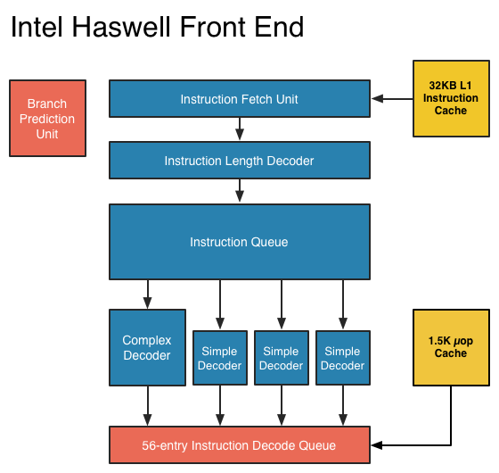
In short, there aren't many major, high-level changes to see here. Instructions are fetched at the top, sent through a bunch of steps before getting to the decoders where they're converted from macro-ops (x86 instructions) to an internally understood format known to Intel as micro-ops (or µops). The instruction fetcher can grab 4 - 5 x86 instructions at a time, and the decoders can output up to 4 micro-ops per clock.
Sandy Bridge introduced the 1.5K µop cache that caches decoded micro-ops. When future instruction fetch requests are made, if the instructions are contained within the µop cache everything north of the cache is powered down and the instructions are serviced from the µop cache. The decode stages are very power hungry so being able to skip them is a boon to power efficiency. There are also performance benefits as well. A hit in the µop cache reduces the effective integer pipeline to 14 stages, the same length as it was in Conroe in 2006. Haswell retains all of these benefits. Even the µop cache size remains unchanged at 1.5K micro-ops (approximately 6KB in size).
Although it's noted above as a new/changed block, the updated instruction decode queue (aka allocation queue) was actually one of the changes made to improve single threaded performance in Ivy Bridge.
The instruction decode queue (where instructions go after they've been decoded) is no longer statically partitioned between the two threads that each core can service.
The big changes in Haswell are at the back end of the pipeline, in the execution engine.


245 Comments
View All Comments
rundll - Friday, October 5, 2012 - link
Four cores and 95 W tdp.What is this?
meloz - Friday, October 5, 2012 - link
Yes this caught my eye and I would like an answer, too.Maybe it is one SKU with GT3 for desktop? Or maybe it is a 6 core part?
Or maybe.....it is the mother of all overclocking processors. Muhahahahah!
Kevin G - Friday, October 5, 2012 - link
I suspect that 95W is the rated socket limit. This is similar to how Intel advertises Ivy Bridge at 77 W on the desktop but tells motherboard manufacturers to build around the higher 95 W figure.What is odd is that Haswell will move some of the VRM circuitry on the package which should restrict just how far off that 95W figure motherboards can deviate.
meloz - Friday, October 5, 2012 - link
What a great article, Anand!Felt so good to read a 'proper' Anandtech article after so long, instead of the usual Apple worship and cheap fillers.
Haswell is looking very good. Would make an ideal upgrade for Sandy Bridge users. AMD is done, but thankfully Intel sees some threat from ARM so that will keep them innovating.
I hope Intel make a sensible choice with Haswell SKUs and get away from their artifical crippling and segmentation tendencies. That's about the only thing that can ruin Haswell.
Wolfpup - Friday, October 5, 2012 - link
Once again they bump up the number of transistors being used on their worthless video-and this time they even lower CPU performance (L3 cache) to appease their worthless video.Interesting article, but I guess I misunderstood previous articles...I thought Conroe through Ivy Bridge had 4 integer execution units per core? (As does Piledriver?)
haukionkannel - Friday, October 5, 2012 - link
Good article and information that you need win 8 to fully utilize Haswell was new information to me. It will be interesting to see how much better Haswell will be with win 8 compared to win 7. Seems to be same kind of dilemma as with AMD Bulldoser/piledriver where there seems to be some kind of better performance with new OS, but how much will reamain to be seen.Belard - Friday, October 5, 2012 - link
Apple owns various CPU tech and design companies such as P.A. Semi. They can build their own CPUs (not x86 of course)...Apple will do what they can to take out the middleman.
jwcalla - Friday, October 5, 2012 - link
Apple doesn't have any fabs though and if Samsung isn't willing to re-sign another contract, they're going to be in a bit of a bind. In other words, it won't be cheap. And even if Samsung does re-up, you can be sure that it'll come with an additional $1.05b price tag to offset any "losses" in their mobile division.I felt the first page overestimated Apple's influence quite a bit. They have ~5% desktop marketshare and 0% in the server space. Not to trivialize any loss in CPU sales, but Intel's primary headwinds don't involve a possible Apple switch to ARM.
Kevin G - Friday, October 5, 2012 - link
Apple's influence comes from the mobile market which is beginning to dwarf the PC market (and is larger than the server market in terms of volume). Apple is the largest tablet maker and a major smart phone manufacturer. There hardware is backed by one of the largest digital media markets. To do this Apple is the worlds largest consumer of flash memory whom orders are large enough to directly affect NAND pricing.With the rest of the industry going ultra mobile, they'll have to compete with Apple who is already entrenched. Sure the PC will survive but mainly for legacy work and applications. Their isn't enough of a PC market in the future to be viable long term with so many players.
jwcalla - Friday, October 5, 2012 - link
While all this is true, the first page seems to indicate that Intel is really pushing the low power envelop partly because of rumors that Apple will move away from Intel chips in their laptop / ultrabook products.While I'm sure Intel is happy to be in MBAs, etc., losing that business isn't going to be as big a deal as the other pressures facing the PC market (as you mention).
Now if WinRT on ultrabooks / laptops began to take off... that would be a huge problem for Intel.