Intel's Haswell Architecture Analyzed: Building a New PC and a New Intel
by Anand Lal Shimpi on October 5, 2012 2:45 AM ESTPrioritizing ILP
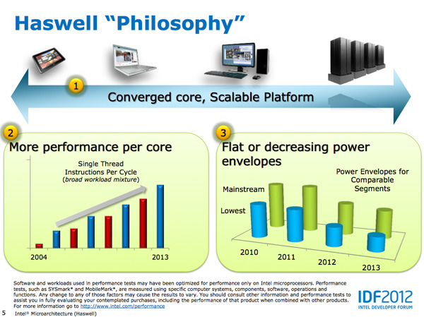
Intel has held the single threaded performance crown for years now, but the why is really quite easy to understand: it has prioritized extracting instruction level parallelism with every generation. Couple that with the fact that every two years we see a "new" microprocessor architecture from Intel and there's a recipe for some good old evolutionary gains. The table below shows the increase in size of some major data structures inside Intel's architectures for every tock since Conroe:
| Intel Core Architecture Buffer Sizes | ||||||
| Conroe | Nehalem | Sandy Bridge | Haswell | |||
| Out-of-order Window | 96 | 128 | 168 | 192 | ||
| In-flight Loads | 32 | 48 | 64 | 72 | ||
| In-flight Stores | 20 | 32 | 36 | 42 | ||
| Scheduler Entries | 32 | 36 | 54 | 60 | ||
| Integer Register File | N/A | N/A | 160 | 168 | ||
| FP Register File | N/A | N/A | 144 | 168 | ||
| Allocation Queue | ? | 28/thread | 28/thread | 56 | ||
Increasing the OoO window allows the execution units to extract more parallelism and thus improve single threaded performance. Each generation Intel is simply dedicating additional transistors to increasing these structures and thus better feeding the beast.
This isn't rocket science, but it is enabled by Intel's clockwork fab execution. Designers can count on another 30% die area to work with every 2 years, so every 2 years they increase the size of these structures without worrying about ballooning the die. The beauty of evolutionary improvements like this is that when viewed over the long term they look downright revolutionary. Comparing Haswell to Conroe, the OoO scheduling window has grown by a factor of 2x, despite generation to generation gains of only 14 - 33%.


245 Comments
View All Comments
kukreknecmi - Friday, October 5, 2012 - link
I hope i know it right. L3 on SB/IB doest used by GPU. L3 still servers as cache on system via memory controller. If GPU nneds to acess to memory, it sends request to memory controller. L3 is not directly accessable to GPU as a texture cache etc.On IB, they added a 512k cache which is seperated to half, 256k of it is used as texture system as backfeeding and other 256k half is used for other things.Article implies that L3 cache on IB is used as a texture buffer like on ordinary graphic cards. Only on Haswell L3 cache will be accessable and can be used as a some kind of GPU specific buffer.
Kevin G - Friday, October 5, 2012 - link
The confusing thing is that consumer Ivy Bridge parts have a L3 cache just for the GPU which is separate memory than the L3 cache that the CPU uses. The Ivy Bridge GPU's can use the CPU's L3 cache as the GPU's L4 cache to a degree.To confuse things further, the CPU side really has four levels of cache too. There is the small 1.5 KB micro-uop cache for instructions which comes before the 32 KB L1 instruction cache.
mayankleoboy1 - Friday, October 5, 2012 - link
From the article, its not very clear : Which platform (DT, Mobile, ultra mobile) will have the integrated voltage regulators/controllers ?Ryan Smith - Friday, October 5, 2012 - link
Ultra Mobile.Anand Lal Shimpi - Friday, October 5, 2012 - link
It's not clear how much of the VR circuitry gets integrated into Haswell or necessarily which parts will have it and which ones won't. Ultra mobile is a shoe in, but I've even heard of desktop parts getting it as well. We'll have to wait and see.DanNeely - Friday, October 5, 2012 - link
Rats. Reading the article I was hoping that Intel had decided to only bake the VRMs into their ultra-mobile parts. Better VRMs are an important factor in high end OCing; with desktop boards not cramped for space I really hope Intel keeps them off the package.Peanutsrevenge - Friday, October 5, 2012 - link
Seconded.However, I wonder whether the VRMs on high end mobos will still be an option, where the on package VRMs will simply extend the capabilities?
But given Intels recent distaste for overclocking, it wouldn't suprise me if we'll soon see CPUs completely locked from overclocking completely or only on E series, high profit chips.
Homeles - Saturday, October 6, 2012 - link
"However, I wonder whether the VRMs on high end mobos will still be an option, where the on package VRMs will simply extend the capabilities?"Bingo.
Homeles - Saturday, October 6, 2012 - link
Low end motherboards won't need them. High end overclocking boards will have them in addition to the ones on package.tuxRoller - Friday, October 5, 2012 - link
Using lvds reclocking you can reduce idle screen induced wakeups to 30 (ditto for the memory controller if the cpu supports self refresh for the sram ).eDP may allow even less.