Intel's Haswell Architecture Analyzed: Building a New PC and a New Intel
by Anand Lal Shimpi on October 5, 2012 2:45 AM ESTFinal Words
After the show many seemed to feel like Intel short changed us at this year's IDF when it came to architecture details and disclosures. The problem is perspective. Shortly after I returned home from the show I heard an interesting comparison: Intel detailed quite a bit about an architecture that wouldn't be shipping for another 9 months, while Apple wouldn't say a thing about an SoC that was shipping in a week. That's probably an extreme comparison given that Apple has no motivation to share details about A6 (yet), but even if you compare Intel's openness at IDF to the rest of the chip makers we cover - there's a striking contrast. We'll always want more from Intel at IDF, but I do hope that we won't see a retreat as the rest of the industry seems to be ok with non-disclosure as standard practice.
There are three conclusions that have to be made when it comes to Haswell: its CPU architecture, its platform architecture and what it means for Intel's future. Two of the three look good from my perspective. The third one is not so clear.
Intel's execution has been relentless since 2006. That's over half a decade of iterating architectures, as promised, roughly once a year. Little, big, little, big, process, architecture, process, architecture, over and over again. It's a combination of great execution on the architecture side combined with great enabling by Intel's manufacturing group. Haswell will continue to carry the torch in this regard.
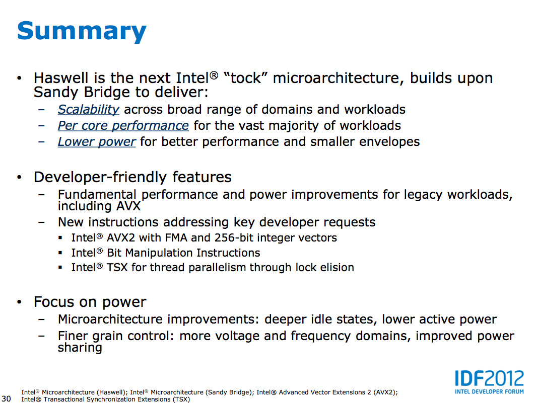
The Haswell micro-architecture focuses primarily on widening the execution engine that has been with us, moderately changed, for the past several years. Increasing data structures and buffers inside the processor helps to feed the beast, as does a tremendous increase in cache bandwidth. Support for new instructions in AVX2 via Intel's TSX should also pave the way for some big performance gains going forward. Power consumption is also a serious target for Haswell given that it must improve performance without dramatically increasing TDP. There will be slight TDP increases across the board for traditional form factors, while ultra portables will obviously shift to lower TDPs. Idle power drops while active power should obviously be higher than Ivy Bridge.
You can expect CPU performance to increase by around 5 - 15% at the same clock speed as Ivy Bridge. Graphics performance will see a far larger boost (at least in the high-end GT3 configuration) of up to 2x vs. Intel's HD 4000 in a standard voltage/TDP system. GPU performance in Ultrabooks will increase by up to 30% over HD 4000.
As a desktop or notebook microprocessor, Haswell looks very good. The architecture remains focused and delivers a sensible set of improvements over its predecessor.
As a platform, Haswell looks awesome. While the standard Haswell parts won't drive platform power down considerably, the new Haswell U/ULT parts will. Intel is promising a greater than 20x reduction in platform idle power and it's planning on delivering it by focusing its power reduction efforts beyond Intel manufactured components. Haswell Ultrabooks and tablets will have Intel's influence in many (most?) of the components placed on the motherboard. And honestly, this is something Intel (or one of its OEMs) should have done long ago. Driving down platform power is a problem that extends beyond the CPU or chipset, and it's one that requires a holistic solution. With Haswell, Intel appears committed to delivering that solution. It's not for purely altruistic reasons, but for the survival of the PC. I remember talking to Vivek about an iPad as a notebook replacement piece he was doing a while back. The biggest advantage the iPad offered over a notebook in his eyes? Battery life. Even for light workloads today's most power efficient ultraportable notebooks can't touch a good ARM based tablet. Haswell U/ULT's significant reduction in platform power is intended to fix that. I don't know that we'll get to 10+ hours of battery life on a single charge, but we should be much better off than we are today.
Connected standby is coming to PCs and it's a truly necessary addition. Haswell's support of active idle states (S0ix) is a game changer for the way portable PCs work. The bigger concern is whether or not the OEMs and ISVs will do their best to really take advantage of what Haswell offers. I know one will, but will the rest? Intel's increasingly hands on approach to OEM relations seems to be its way of ensuring we'll see Haswell live up to its potential.
Haswell, on paper, appears to do everything Intel needs to evolve the mobile PC platform. What's unclear is how far down the TDP stack Intel will be able to take the architecture. Intel seems to believe that TDPs below 8W are attainable, but it's too early to tell just how low Haswell can go. It's more than likely that Intel knows and just doesn't want to share at this point. I don't believe we'll see fanless Haswell designs, but Broadwell is another story entirely.
There's no diagram for where we go from here. Intel originally claimed that Atom would service an expanded range of TDPs all the way up to 10W. With Core architectures dipping below 10W, I do wonder if that slide was a bit of misdirection. I wonder if, instead, the real goal is to drive Core well into Atom territory. If Intel wants to solve its ARM problem, that would appear to be a very good solution.


245 Comments
View All Comments
kukreknecmi - Friday, October 5, 2012 - link
I hope i know it right. L3 on SB/IB doest used by GPU. L3 still servers as cache on system via memory controller. If GPU nneds to acess to memory, it sends request to memory controller. L3 is not directly accessable to GPU as a texture cache etc.On IB, they added a 512k cache which is seperated to half, 256k of it is used as texture system as backfeeding and other 256k half is used for other things.Article implies that L3 cache on IB is used as a texture buffer like on ordinary graphic cards. Only on Haswell L3 cache will be accessable and can be used as a some kind of GPU specific buffer.
Kevin G - Friday, October 5, 2012 - link
The confusing thing is that consumer Ivy Bridge parts have a L3 cache just for the GPU which is separate memory than the L3 cache that the CPU uses. The Ivy Bridge GPU's can use the CPU's L3 cache as the GPU's L4 cache to a degree.To confuse things further, the CPU side really has four levels of cache too. There is the small 1.5 KB micro-uop cache for instructions which comes before the 32 KB L1 instruction cache.
mayankleoboy1 - Friday, October 5, 2012 - link
From the article, its not very clear : Which platform (DT, Mobile, ultra mobile) will have the integrated voltage regulators/controllers ?Ryan Smith - Friday, October 5, 2012 - link
Ultra Mobile.Anand Lal Shimpi - Friday, October 5, 2012 - link
It's not clear how much of the VR circuitry gets integrated into Haswell or necessarily which parts will have it and which ones won't. Ultra mobile is a shoe in, but I've even heard of desktop parts getting it as well. We'll have to wait and see.DanNeely - Friday, October 5, 2012 - link
Rats. Reading the article I was hoping that Intel had decided to only bake the VRMs into their ultra-mobile parts. Better VRMs are an important factor in high end OCing; with desktop boards not cramped for space I really hope Intel keeps them off the package.Peanutsrevenge - Friday, October 5, 2012 - link
Seconded.However, I wonder whether the VRMs on high end mobos will still be an option, where the on package VRMs will simply extend the capabilities?
But given Intels recent distaste for overclocking, it wouldn't suprise me if we'll soon see CPUs completely locked from overclocking completely or only on E series, high profit chips.
Homeles - Saturday, October 6, 2012 - link
"However, I wonder whether the VRMs on high end mobos will still be an option, where the on package VRMs will simply extend the capabilities?"Bingo.
Homeles - Saturday, October 6, 2012 - link
Low end motherboards won't need them. High end overclocking boards will have them in addition to the ones on package.tuxRoller - Friday, October 5, 2012 - link
Using lvds reclocking you can reduce idle screen induced wakeups to 30 (ditto for the memory controller if the cpu supports self refresh for the sram ).eDP may allow even less.